

Page 1

PRELIMINARY PRODUCT SPECIFICATION
nRF24Z1
SUNSTAR单片机专用电路 http://www.icasic.com/ TEL: 0755-83387030 FAX:0755-83376182 E-MAIL:szss20@163.com
SUNSTAR半导体集成电路 http://www.icasic.com/ TEL: 0755-83387016 FAX:0755-83376182 E-MAIL:szss20@163.com
2.4GHz wireless audio streamer
FEATURES APPLICATIONS
• Low cost 0.18u CMOS process, 36 pin 6x6mm
QFN package
• Single chip 2.4GHz RF transceiver • MP3 / Mini Disk headset
• 4Mbit/sec RF link • Speakers
• Input sample rate up to 96kHz, 24bits • Surround speakers
• Output sample rate up to 48kHz, 16bits • Microphone
• Programmable latency • Musical instruments
• Quality of Service engine supporting up to
1.536 Mbit/s LPCM audio
• S/PDIF interface for direct connection to PC
soundcard and surround receivers
• I2S interface for glueless audio support • Compressed video streaming
• SPI or 2-wire interface for up to 12 kbit/sec peak bi-
directional digital control/AUX data
• On chip optional 2:1 compression
• On chip voltage regulators
• Few external components
• Uses global 2.4GHz band
• Compact Disk, CD quality
headset
• Audio streaming from PC
soundcard to HiFi system
• Download MP3 files from PC
to MP3 player
GENERAL DESCRIPTION
nRF24Z1 gives you a true single chip system for CD quality audio streaming of up to16 bit
48 kHz audio with support of up to 24 bit 96 kHz input. I2S and S/PDIF interfaces are
supported for audio I/O. Seamless interfacing of low cost A/D and D/A for analog audio
input and output. SPI or 2-wire (I2C compatible) serial interfaces for control. The circuit
has embedded voltage regulators, giving maximum noise immuni ty and operation from a
single 2.0V to 3.6V supply.
QUICK REFERENCE DATA
Parameter Value Unit
Minimum supply voltage 2.0 V
Temperature range -20 to +80
Peak supply current in transmit @ -5dBm output power 15 mA
Peak supply current in receive mode 32 mA
Supply current in power down mode 4 µA
Maximum transmit output power 0 dBm
Audio sample rate 32, 44.1 or 48 kbps
Audio resolution 16 bit
Receiver sensitivity -80 dBm
Table 1-1 nRF24Z1 quick reference data.
°C
Page 2

PRELIMINARY PRODUCT SPECIFICATION
SUNSTAR单片机专用电路 http://www.icasic.com/ TEL: 0755-83387030 FAX:0755-83376182 E-MAIL:szss20@163.com
SUNSTAR半导体集成电路 http://www.icasic.com/ TEL: 0755-83387016 FAX:0755-83376182 E-MAIL:szss20@163.com
nRF24Z1 wireless audio streamer
ORDERING INFORMATION
Type number Description Version
nRF24Z1 36L QFN 6x6 mm A
nRF24Z1-EVKIT Evaluation kit 1.0
Table 1-2 nRF24Z1 ordering information.
Page 3

PRELIMINARY PRODUCT SPECIFICATION
SUNSTAR单片机专用电路 http://www.icasic.com/ TEL: 0755-83387030 FAX:0755-83376182 E-MAIL:szss20@163.com
SUNSTAR半导体集成电路 http://www.icasic.com/ TEL: 0755-83387016 FAX:0755-83376182 E-MAIL:szss20@163.com
nRF24Z1 wireless audio streamer
TABLE OF CONTENTS
FEATURES ............................................................................................................................1
APPLICATIONS ....................................................................................................................1
GENERAL DESCRIPTION...................................................................................................1
QUICK REFERENCE DATA................................................................................................1
ORDERING INFORMATION...............................................................................................2
TABLE OF CONTENTS........................................................................................................3
1 Pin Assignment ...............................................................................................................6
2 Pin Function....................................................................................................................7
3 Glossary of terms ............................................................................................................8
4 Architectural Overview...................................................................................................9
4.1 Audio transmitter ..................................................................................................11
4.1.1 I2S audio input..............................................................................................11
4.1.2 S/PDIF audio input .......................................................................................12
4.1.3 Serial control (slave) interfaces.....................................................................12
4.1.4 Master interfaces...........................................................................................12
4.1.5 Direct data input pins ....................................................................................13
4.1.6 Interrupt output .............................................................................................13
4.2 Audio Receiver .....................................................................................................13
4.2.1 I2S audio output............................................................................................14
4.2.2 S/PDIF audio output.....................................................................................15
4.2.3 Master interfaces...........................................................................................15
4.2.4 Serial control (slave) interfaces.....................................................................15
4.2.5 Parallel port and PWM..................................................................................15
4.3 Blocks common to audio transmitter and receiver................................................16
4.3.1 XTAL Oscillator ...........................................................................................16
4.3.2 Radio Transceiver.........................................................................................16
4.3.3 Quality of Service engine..............................................................................16
4.3.4 Audio compression / Decompression...........................................................17
4.3.5 Power............................................................................................................17
4.3.6 IREF / RESET...............................................................................................17
5 Operation overview.......................................................................................................18
5.1 Power on / RESET sequence ................................................................................18
5.2 RF Link initialization............................................................................................18
5.2.1 Idle state ........................................................................................................18
5.2.2 Link-locate state............................................................................................19
5.2.3 Synchronization state ....................................................................................19
5.3 Audio streaming....................................................................................................19
5.4 Audio receiver clock rate recovery.......................................................................20
5.5 Data link................................................................................................................20
5.6 Power down mode.................................................................................................21
6 nRF24Z1 register MAP.................................................................................................22
6.1 Access from audio transmitter side.......................................................................22
6.2 Access from audio receiver side ...........................................................................22
7 Digital I/O.....................................................................................................................25
7.1 Digital I/O behaviour during RESET....................................................................25
Page 4

PRELIMINARY PRODUCT SPECIFICATION
SUNSTAR单片机专用电路 http://www.icasic.com/ TEL: 0755-83387030 FAX:0755-83376182 E-MAIL:szss20@163.com
SUNSTAR半导体集成电路 http://www.icasic.com/ TEL: 0755-83387016 FAX:0755-83376182 E-MAIL:szss20@163.com
nRF24Z1 wireless audio streamer
7.2 Audio interfaces....................................................................................................25
7.3 I2S Audio Interface...............................................................................................25
7.4 S/PDIF Audio Interface ........................................................................................26
7.5 Audio interface functionality ................................................................................27
7.5.1 ATX audio interface control.........................................................................27
7.5.2 ARX audio interface control.........................................................................30
7.5.3 I2S Audio interface timing............................................................................32
7.6 Serial master interfaces.........................................................................................33
7.6.1 Timing serial master interfaces....................................................................36
7.7 Control and GPIO interfaces.................................................................................37
7.7.1 ATX control and GPIO pins .........................................................................37
7.7.2 SPI slave interface.........................................................................................38
7.7.3 2-wire slave interface....................................................................................38
7.7.4 General purpose input pins D[2:0]................................................................40
7.7.5 ATX Control interface timing.......................................................................41
7.7.6 ARX control interface options ......................................................................42
7.7.7 ARX GPIO pins ............................................................................................43
7.8 Data Channel Timing............................................................................................45
7.8.1 Forward data channel, data transfer from ATX to ARX...............................45
7.8.2 Return data channel, data transfer from ARX to ATX .................................46
8 Quality of service (Qos) and RF...................................................................................48
8.1 Link algorithm.......................................................................................................48
8.2 RF protocol ...........................................................................................................48
8.3 Adaptive frequency hopping.................................................................................48
8.3.1 Adapting to the RF environment...................................................................50
8.4 Link registers.........................................................................................................50
8.4.1 RF link latency..............................................................................................52
8.5 RF output power ...................................................................................................53
9 Interrupts .......................................................................................................................54
10 RESET outputs..........................................................................................................55
11 Power down control..................................................................................................56
11.1 Enter power down.................................................................................................56
11.2 Wake up from power down...................................................................................56
11.2.1 External pin change.......................................................................................57
11.2.2 Timer controlled wake up .............................................................................57
11.3 nRF24Z1 power saving example ..........................................................................58
12 Register update over the data link.............................................................................60
13 Eletrical Specification...............................................................................................61
14 Absolute maximum ratings .......................................................................................63
15 Package outline .........................................................................................................64
16 Application Information............................................................................................65
16.1 Antenna I/O...........................................................................................................65
16.2 Crystal Specification.............................................................................................65
16.3 Bias reference resistor...........................................................................................65
16.4 Internal digital supply de-coupling .......................................................................65
16.5 PCB layout and de-coupling guidelines................................................................66
17 Application example.................................................................................................67
17.1 nRF24Z1 schematics.............................................................................................67
Page 5

PRELIMINARY PRODUCT SPECIFICATION
SUNSTAR单片机专用电路 http://www.icasic.com/ TEL: 0755-83387030 FAX:0755-83376182 E-MAIL:szss20@163.com
SUNSTAR半导体集成电路 http://www.icasic.com/ TEL: 0755-83387016 FAX:0755-83376182 E-MAIL:szss20@163.com
nRF24Z1 wireless audio streamer
17.2 nRF24Z1 layout....................................................................................................69
17.3 nRF24Z1 Bill of Material .....................................................................................71
18 References.................................................................................................................73
19 Definitions.................................................................................................................74
20 Your notes .................................................................................................................75
Page 6

PRELIMINARY PRODUCT SPECIFICATION
SUNSTAR单片机专用电路 http://www.icasic.com/ TEL: 0755-83387030 FAX:0755-83376182 E-MAIL:szss20@163.com
SUNSTAR半导体集成电路 http://www.icasic.com/ TEL: 0755-83387016 FAX:0755-83376182 E-MAIL:szss20@163.com
nRF24Z1 wireless audio streamer
1 PIN ASSIGNMENT
DO[3]/
IRQ/
MSCK
VSS
VDD
PWM
MMOSI
VSS
MMISO
MCSN
MSCL
SSEL/DO[2]
SMISO/SSDA/DO[1]
SSCK/SSCL/DO[0]
SCSN/SADR/DI[3]
VDD
SMOSI/DD[2]/DI[2]
DD[1]/DI[1]
DD[0]/DI[0]
REQ
32
1
2
3
nRF24Z1
2829303136 35 34 33
27
MSDA
26
MODE
25
VSS
QFN36 6x6
IREF
4
5
6
7
8
9
1817161510 11 12 13 14
XC1
XC2
VSS
CLK
WS
DATA
SPDIO
MCLK
DVDD
24
23
VSS_PA
ANT2
22
21
ANT1
VDD_PA
20
19
VDD
Figure 1-1: Pin assignment nRF24Z1
Page 7

PRELIMINARY PRODUCT SPECIFICATION
Pin function
SUNSTAR单片机专用电路 http://www.icasic.com/ TEL: 0755-83387030 FAX:0755-83376182 E-MAIL:szss20@163.com
SUNSTAR半导体集成电路 http://www.icasic.com/ TEL: 0755-83387016 FAX:0755-83376182 E-MAIL:szss20@163.com
nRF24Z1 wireless audio streamer
2 PIN FUNCTION
Name
Description Pin
Slave
IF
1 SSEL DO[2] Dig. In Dig. Out Slave interface select
2 SMISO
/SSDA
3 SSCK
/SSCL
4 SCSN
/SADR
5 VDD Power Power Supply (2.0-3.6 V DC)
6 SMOSI
/DD[2]
7 DD[1] DI1 Digital Input Direct data in bit #1 GPIO in bit #1
8 DD[0] DI0 Digital Input Direct data in bit #0 GPIO in bit #0
9 REQ Dig. Out Dig. In I2S data request (programmable polarity)
10 CLK Dig. In Dig. Out I2S bit clock
11 WS Dig. In Dig. Out I2S word clock
12 DATA Dig. In Dig. Out I2S data signal
13 SPDIO Dig. In Dig. Out S/PDIF interface
14 MCLK Dig. Out 256X sample rate clock to ADC or DAC
15 DVDD Regulator output Digital voltage regulator output for decoupling
16 VSS Power Ground (0V)
17 XC2 Analog output Crystal Pin 2
18 XC1 Analog input Crystal Pin 1
19 VDD Power Power Supply (2.0-3.6 V DC)
20 VDD_PA Regulator output DC output (+1.8V) for RF interface (ANT1, ANT2)
21 ANT1 RF Antenna interface 1
22 ANT2 RF Antenna interface 2
23 VSS_PA Power Ground (0V)
24 IREF Analog input Connection to external Bias reference resistor, or RESET
25 VSS Power Ground (0V)
26 MODE Digital Input nRF24Z1 function
27 MSDA Digital IO Master 2-wire bi-directional data
28 MSCL Digital IO Master 2-wire bi-directional clock
29 MCSN Digital Output Master SPI primary slave select (active low)
30 MMISO Digital Input Master SPI serial input
31 MMOSI Digital Output Master SPI serial output
32 VSS Power Ground (0V)
33 VDD Power Power Supply (2.0-3.6 V DC)
34 VSS Power Ground (0V)
35 MSCK Digital Output Master SPI clock
36 IRQ DO[3]
ARX
GPIO Slave IF
DO[1] Digital Output
/ Digital IO
DO[0] Dig. In Dig. Out Slave SPI clock
DI3 Digital Input Slave SPI slave select
DI2 Digital Input Slave SPI serial in
Digital Output Interrupt request GPIO out bit #3
/ PWM
ARX
GPIO IF ATX/ARX with slave IF
1: 2-wire, 0: SPI
Slave SPI serial out
/ Slave 2-wire data (bidir)
/ Slave 2-wire clock
/ Address select 2-wire slave
/ Direct data in bit #2
if pulled to VDD
1 : audio transmitter, 0: audio receiver
ARX with GPIO IF
GPIO out bit #2
GPIO out bit #1
GPIO out bit #0
GPIO in bit #2
GPIO in bit #3
/ PWM output
Table 2-1 nRF24Z1 pin function
Page 8

PRELIMINARY PRODUCT SPECIFICATION
SUNSTAR单片机专用电路 http://www.icasic.com/ TEL: 0755-83387030 FAX:0755-83376182 E-MAIL:szss20@163.com
SUNSTAR半导体集成电路 http://www.icasic.com/ TEL: 0755-83387016 FAX:0755-83376182 E-MAIL:szss20@163.com
nRF24Z1 wireless audio streamer
3 GLOSSARY OF TERMS
Term Description
ADC Analog to Digital Converter
ARX audio receiver
ATX audio transmitter
CD Carrier Detect
CHPA SPI clock phase
CLK Clock
CPOL SPI clock polarity
CRC Cyclic Redundancy Check
DAC Digital to Analog Converter
DSP Digital Signal Processor
EEPROM electrical erasable programmable read only
memory
Flash Flash memory
GFSK Gaussian Frequency Shift Keying
GPIO General Purpose In Out
I2S 3 wire audio serial interface
ISM Industrial-Scientific-Medical
LPCM linear PCM (pulse code modulation)
MBZ Must Be Zero (reserved for future extensions)
MCU Micro Controller Unit
MP3 a popular compressed audio format
PWM Pulse Width Modulation
QOS Quality Of Service
RX Receive
S/PDIF one wire serial digital audio format
SPI Serial Peripheral Interface
TX Transmit
2-wire 2-wire serial interface compatible with I2C
Table 3-1 Glossary of terms nRF24Z1.
Page 9
PRELIMINARY PRODUCT SPECIFICATION
SUNSTAR单片机专用电路 http://www.icasic.com/ TEL: 0755-83387030 FAX:0755-83376182 E-MAIL:szss20@163.com
SUNSTAR半导体集成电路 http://www.icasic.com/ TEL: 0755-83387016 FAX:0755-83376182 E-MAIL:szss20@163.com
nRF24Z1 wireless audio streamer
4 ARCHITECTURAL OVERVIEW
nRF24Z1 is a 4 MBit/s single chip RF transceiver that operates in the world wide 2.4 GHz
licencee free ISM band. The nR24Z1 is based on the proven nRF24xx radio and
ShockBurst™ platforms from Nordic Semiconductor.
The device offers a wireless channel for seamless streaming of LPCM or compressed audio
in parallel with a low data rate control channel. To enable this, the device offers the
following features in addition to the nRF24xx RF platform:
• Standard digital audio interfaces (I2S, S/PDIF)
• Fully embedded Quality of Service engine that handles all RF protocol and
RF link tasks.
• SPI and 2-wire master and slave control interfaces
• GPIO pins
As all processing related to audio I/O, RF protocol and RF link management is embedded,
the device offers the end application an up to 1.54 MBit/s transparent audio channel
without any true time processing needed. nRF24Z1 can be utilized in systems without
external microcontroller or by a simple microcontroller that only need to handle low speed
tasks over the serial or parallel ports (ex: volume up/down).
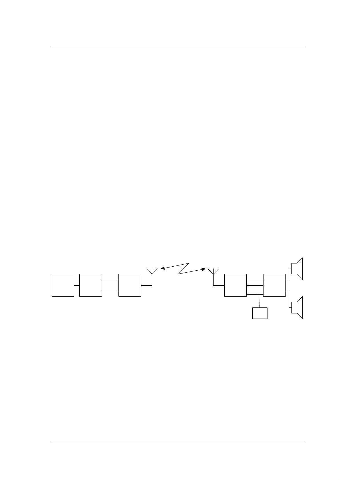
A typical system using nRF24Z1 can be seen in Figure 4-1
Audio Source Destination
DAC
and
audio
amplifier
E2
Storage
DSP /
uP
nRF24Z1 nRF24Z1
I2S
Audio
transmitter
MCLKSPI
I2S
SPI
Audio
receiver
Figure 4-1 Typical audio application using nRF24Z1
In this system a DSP or micro controller feeds data from storage to nRF24Z1 using
standard audio format (I2S). A nRF24Z1 pair transfers the audio data and presents it to a
stereo DAC on the other side. For other parts of the application, the nRF24Z1 link will in
other words look like an open channel (like a cable).
Initial configuration of nRF24Z1 is done by the micro controller through a SPI or 2-wire
control interface. On the destination side, peripherals like a DAC can be controlled from
the audio source side through the control channel offered by nRF24Z1. In designs without
an external micro controller, configuration data can be loaded by nRF24Z1 from an
optional EEPROM/FLASH memory, enabling it to operate stand alone with limited feature
set.
Page 10

PRELIMINARY PRODUCT SPECIFICATION
SUNSTAR单片机专用电路 http://www.icasic.com/ TEL: 0755-83387030 FAX:0755-83376182 E-MAIL:szss20@163.com
SUNSTAR半导体集成电路 http://www.icasic.com/ TEL: 0755-83387016 FAX:0755-83376182 E-MAIL:szss20@163.com
nRF24Z1 wireless audio streamer
A wireless system that is streaming audio will have a very asymmetrical load on the RF
link since audio data is fed from an audio source (CD player) to a destination (loud
speakers). From the destination back to the audio source only service and control
communication is needed.
nRF24Z1 are used both on the audio source side (ex. in a CD player) transmitting audio
data, and in the 'destination' (loud speaker) side receiving audio data. Due to the
asymmetry, nRF24Z1 has two main modes set by external pin MODE, depending on which
side of the link it is put. The two modes have significant differences both in internal and
I/O functionality.
To ease understanding of nRF24Z1 operation, the following notation is introduced:
• Audio transmitter (ATX) – nRF24Z1 on the audio source side, transmitting audio data
• Audio receiver (ARX ) – nRF24Z1 on the destination side, receiving audio data
Transmitter and receiver are here referring to the flow of the audio; the nRF24Z1 RF front
end always runs a full two way link.
The nRF24Z1 control and data channel is a two way low data rate channel superimposed on
the audio and service communication. The audio transmitter is designated master meaning
that when a RF link is present 2-wire, SPI, GPIO and internal registers in the audio receiver
can be seen and controlled as a virtual extension of the audio transmitters own I/O and
registers. The implications of this is that external devices like audio DAC or volume control
components connected to the audio receiver effectively can be controlled by input to the
audio transmitter. User actions (ex: push of a button) on the audio receiver side are
similarly fed back to and can be processed on the audio transmitter side.
The following sections will give an overview of the I/O, main modules and functionality of
nRF24Z1. Due to the differences in ATX and ARX, the overview will present the modes
separately.
Page 11

PRELIMINARY PRODUCT SPECIFICATION
SUNSTAR单片机专用电路 http://www.icasic.com/ TEL: 0755-83387030 FAX:0755-83376182 E-MAIL:szss20@163.com
SUNSTAR半导体集成电路 http://www.icasic.com/ TEL: 0755-83387016 FAX:0755-83376182 E-MAIL:szss20@163.com
nRF24Z1 wireless audio streamer
4.1 Audio transmitter
When nRF24Z1 is put at the audio source side of the RF link, MODE must be high and
nRF24Z1 becomes an audio transmitter (ATX). The block schematic of nRF24Z1 in ATX
mode can be seen in Figure 4-2.
VDD
DVDD
VSS
SADR/
SCSN
SSCL/
SSCK
SSDA/
SMISO
SMOSI/
DD[2]
SSEL
DD[1:0]
IRQ
SPDIO
CLK
DATA
WS
REQ
POWER
Slave
IF
MUX
S/PDIF
to
I2S
2-wire
slave
SPI
slave
parallel
Serial
to
Local
Status
Local
Config
Remote
Status
Remote
Config
Remote
Data
Audio
compress
MUX
TDM
QOS
2-wire
master
SPI
master
nRF
24xx
radio
BIAS /
RESET
MSDA
MSCL
MMISO
MSCK
MMOSI
MCSN
VSS_PA
ANT1
ANT2
VDD_PA
IREF
PLLMCLK
Clock
Control
XTAL
oscillator
XC2
XC1
Figure 4-2 nRF24Z1 ATX mode block diagram
The I2S or S/PDIF interfaces can be used for audio data input or alternatively the device
may stream other real-time data from a DSP over the I2S interface.
4.1.1 I2S audio input
For seamless input from audio sources physically close to nRF24Z1, I2S is the preferred
interface. The I2S interface consists of pins CLK, DATA and WS. The interface supports
Page 12

PRELIMINARY PRODUCT SPECIFICATION
SUNSTAR单片机专用电路 http://www.icasic.com/ TEL: 0755-83387030 FAX:0755-83376182 E-MAIL:szss20@163.com
SUNSTAR半导体集成电路 http://www.icasic.com/ TEL: 0755-83387016 FAX:0755-83376182 E-MAIL:szss20@163.com
nRF24Z1 wireless audio streamer
sample rates of 32, 44.1, 48 and 96 kHz. Data may be in 16, 20 or 24 bit format.1 The data
rate is automatically detected.
I2S may also be used with an external stereo ADC for analog audio sources. The nRF24Z1
offers a 256 times audio sampling rate clock (fS) on the MCLK pin to be used as system
clock for the ADC.
A REQ output is available for pacing the data-flow when streaming MP3 and other “data”
streams over the I2S interface.
4.1.2 S/PDIF audio input
For audio sources physically more remote , the ATX offers a (CMOS level) S/PDIF input
on pin SPDIO. This interface supports 32, 44.1 or 48 kHz sampling rates with resolution of
16, 20 or 24 bit. It supports both linear and nonlinear audio according to IEC standards, see
ch. 7.4 for details.
4.1.3 Serial control (slave) interfaces
When ATX is controlled by an external MCU, configuration and control data both for the
audio transmitter itself and a linked audio receiver may be entered via a 2-wire or SPI slave
serial interface. The same interface is used for reading back status information. The register
map is identical for both interfaces, but only one of the interfaces, selected by SSEL pin,
may be used in a given application.
The two interfaces are :
SSEL = 0; SPI (pins SCSN, SSCK, SMISO, SMOSI).
SSEL = 1; 2-wire (pins SADR, SSCL and SSDA)
Pin SADR is not part of a standard 2-wire interface but selects one of two possible bus
addresses for the nRF24Z1.
4.1.4 Master interfaces
For standalone operation of nRF24Z1, a serial EEPROM or FLASH memory may be
connected to a SPI or 2-wire master interface. If a memory is present at any of these
interfaces during power up or reset, the device will read default configuration data from the
memory.
The SPI master is found on pins MCSN, MMISO, MMOSI and MSCK and 2-wire master
on pins MSDA and MSCL.
1
This specification item is for the I2S input interface. Not all of these formats can be
transferred within the available 1.54 Mbit/s data rate.
Page 13

PRELIMINARY PRODUCT SPECIFICATION
SUNSTAR单片机专用电路 http://www.icasic.com/ TEL: 0755-83387030 FAX:0755-83376182 E-MAIL:szss20@163.com
SUNSTAR半导体集成电路 http://www.icasic.com/ TEL: 0755-83387016 FAX:0755-83376182 E-MAIL:szss20@163.com
nRF24Z1 wireless audio streamer
4.1.5 Direct data input pins
The ATX has 2 general purpose input pins, DD[1:0], that may be transmitted directly to
and hence mirrored on the audio receiver. When SSEL is set high (2-wire interface
selected), one additional direct data pin (DD[2]) is available. If the logic level on pins
DD[2:0] are mirrored (copied) over the control link, pins DO[2:0] on the audio receiver
will carry the mirrored signal.
These pins may hence be used to switch on/off audio receiver peripherals without
microprocessor activity.
4.1.6 Interrupt output
The nRF24Z1 can interrupt the external application through pin IRQ based on a number of
sources such as no audio input detected, loss of RF communication etc.
Once IRQ has triggered external MCU, interrupt status can be read, through the serial
control interface.
4.2 Audio Receiver
When nRF24Z1 is put at the destination side of the RF link, MODE must be low and
nRF24Z1 becomes the audio receiver (ARX). The block schematic of nRF24Z1 in ARX
mode can be seen in Figure 4-3. I2S or S/PDIF are now used for audio or other real time
data output.
Page 14

PRELIMINARY PRODUCT SPECIFICATION
SUNSTAR单片机专用电路 http://www.icasic.com/ TEL: 0755-83387030 FAX:0755-83376182 E-MAIL:szss20@163.com
SUNSTAR半导体集成电路 http://www.icasic.com/ TEL: 0755-83387016 FAX:0755-83376182 E-MAIL:szss20@163.com
nRF24Z1 wireless audio streamer
VDD
DVDD
VSS
VSS_PA
ANT1
ANT2
VDD_PA
IREF
POWER
nRF
24xx
radio
BIAS /
RESET
TDM
QOS
Audio de-
compress
PWM
MUX
MUX
Parallel
to
serial
2-wire
master
SPI
master
I2S
to
SPDIF
MSDA
MSCL
MMISO
MSCK
MMOSI
MCSN
DI[3:0]
DO[3:0]
SPDIO
CLK
DATA
WS
REQ
XC2
XC1
XTAL
oscillator
Clock
Control
PLL /
MUX
MCLK
Figure 4-3 nRF24Z1 ARX mode block diagram
After a link is established the user can control the SPI and 2 wire master from the audio
transmitter. In this way the audio transmitter is able to control audio receiver serial
peripherals like audio DACs and amplifiers.
4.2.1 I2S audio output
Audio output to devices physically close to nRF24Z1 (typically a stereo DAC) are normally
driven by the I2S output (pins CLK, DATA and WS). The inte rface supports sample rates
of 32, 44.1 and 48 kHz. Data are in 16 bit format.
In audio receiver mode the MCLK pin provides 256 times fS clock for an external DAC.
A REQ input is available for pacing the data-flow when streaming MP3 or other “data”
streams over the I2S.
Page 15

PRELIMINARY PRODUCT SPECIFICATION
SUNSTAR单片机专用电路 http://www.icasic.com/ TEL: 0755-83387030 FAX:0755-83376182 E-MAIL:szss20@163.com
SUNSTAR半导体集成电路 http://www.icasic.com/ TEL: 0755-83387016 FAX:0755-83376182 E-MAIL:szss20@163.com
nRF24Z1 wireless audio streamer
4.2.2 S/PDIF audio output
For physically more remote audio devices, the audio receiver provides an S/PDIF (full
swing CMOS) output on pin SPDIO. This interface supports 32, 44.1 and 48 kHz, 16 or 24
bit data. It supports both linear and nonlinear audio according to IEC standards, see ch. 7.4
for details.
4.2.3 Master interfaces
A serial EEPROM or FLASH memory may be connected to a SPI or 2-wire master
interface. If a memory is present at any of these interfaces during power up or reset, the
device will read default configuration data from that memory; otherwise hard coded default
values will be used.
During audio receiver configuration, the SPI master (pins MMSCK, MMISO, MMOSI,
MCSN) is operated at 1MHz or 0.5MHz with the SPI format set to CPOL=0,CHPA=0 for
EEPROM/FLASH compatibility. After a link is established, the user may control the SPI
master from the audio transmitter. The available clock speed is up to 8 MHz over the full
operation range of the device.
During start-up, the audio receiver operates the 2-wire master (MSDA, MSCL) interface at
100 kHz. After a link is established, the user may control the 2-wire master from the audio
transmitter to 100kHz, 400kHz or 1MHz.
4.2.4 Serial control (slave) interfaces
When ARX is controlled by an external MCU, configuration and control data for the audio
receiver may be entered via a 2-wire or SPI slave serial interface. The same interface is
used for reading back status information. The register map is identical for both interfaces,
but only one of the interfaces, selected by SSEL pin, may be used in a given application.
The two interfaces are :
SSEL = 0; SPI (pins SCSN, SSCK, SMISO, SMOSI).
SSEL = 1; 2-wire (pins SADR, SSCL and SSDA)
Pin SADR is not part of a standard 2-wire interface but selects one of two possible bus
addresses for the nRF24Z1.
4.2.5 Parallel port and PWM
Alternatively to the serial slave interfaces, ARX can be configured with an 8 bit parallel
port, which can be controlled and read from the audio transmitter. There are 4 input pins
DI[3:0] that are continuously monitored when a link is up. Changes on any of these inputs
will be sent back to the audio transmitter where it can be accessed in a register (via the
serial control interface). The audio receiver can also be programmed to wake up from
power down mode on a change on one of these pins.
Page 16

PRELIMINARY PRODUCT SPECIFICATION
SUNSTAR单片机专用电路 http://www.icasic.com/ TEL: 0755-83387030 FAX:0755-83376182 E-MAIL:szss20@163.com
SUNSTAR半导体集成电路 http://www.icasic.com/ TEL: 0755-83387016 FAX:0755-83376182 E-MAIL:szss20@163.com
nRF24Z1 wireless audio streamer
There are 4 outputs DO[3:0] that are controlled from the audio transmitter. Any of these
may be programmed for high current in order to drive LEDs or for standard CMOS to
control of other devices on the audio receiver board.
DO3 may be programmed to output a PWM signal, where the output duty cycle is
programmable with 8-bit resolution from the audio transmitter. Note that this PWM cannot
be used as audio DAC
The output pins DO[3:0] may also function as slave select signals if multiple slaves are
present on the ARX SPI master bus.
4.3 Blocks common to audio transmitter and receiver
4.3.1 XTAL Oscillator
The crystal oscillator will provide a stable reference frequency with low phase noise for the
radio and audio functions. See section 16.2 for full Crystal Specification.
4.3.2 Radio Transceiver
The RF transceiver part of the circuit is a member of nRF24xx family of low power highly
integrated 2.4GHz ShockBurst™ transceivers. The transceiver interface is optimized for
high speed streaming of up to 4 Mbps. Output power and some protocol parameters can be
controlled by the user via the QoS module.
4.3.3 Quality of Service engine
The primary function of the quality of service engine is to deliver a robust communication
channel between the audio transmitter and audio receiver in an audio streaming application.
Several data streams with different properties are handled. The available bandwidth is
shared between audio data, service data and remote data.
Data integrity is ensured through a number of RF protocol features:
1. Packets of data are sent in frames and integrity of each packet is ensured as every
packet has a complete build of RF address, payload and CRC.
2. Packets that are lost or received with errors are handled by the error correction level
of the quality of service engine; a two way, acknowledge protocol:
When a packet is received by ARX, it’s registered and CRC is checked.
After ARX has received a frame it sends a packet back to ATX
acknowledging the packets that where successfully transferred. Packets lost
or received with errors will be re-sent from ATX in the next frame.
3. Finally the information (audio data ) is spread over the 2.4 GHz band by use of an
adaptive frequency hopping algorithm. Through this a nRF24Z1 link can handle RF
propagation challenges like reflections and multi-path fading and not least avoid
Page 17

PRELIMINARY PRODUCT SPECIFICATION
SUNSTAR单片机专用电路 http://www.icasic.com/ TEL: 0755-83387030 FAX:0755-83376182 E-MAIL:szss20@163.com
SUNSTAR半导体集成电路 http://www.icasic.com/ TEL: 0755-83387016 FAX:0755-83376182 E-MAIL:szss20@163.com
nRF24Z1 wireless audio streamer
heavily trafficked areas of the 2.4 GHz band. The 2.4 GHz band is a world wide
open RF band and co-existence with RF systems such as Bluetooth, ZigBee,
WLAN/WiFi as well as other nRF applications, is increasingly important.
nRF24Z1 constantly monitors the quality of the RF link and numbers indicating total link
quality are available for external control devices in registers. nRF24Z1 can also be set to
interrupt external controller devices upon poor link quality before RF link is lost. An
external controller device can hence take further actions to improve link quality or warn
end user if RF link margins are poor.
The secondary function of the QoS module is to run a link initialization algorithm which
manages initial connect and re-connect if link is lost (ex: out of range) between paired
nRF24Z1’s. Several schemes are available to enable nRF24Z1 connection without end user
involvement.
4.3.4 Audio compression / Decompression
Default operation for nRF24Z1 is streaming of uncompressed audio, however there is some
optional low delay audio compression options available. This function can be enabled by
the user to conserve power or to increase the dynamic range with a constant signal to noise
ratio for 24-bit input signals.
4.3.5 Power
The power section of nRF24Z1 offers linear regulated supply to all internal parts of the
device. This makes the device very robust towards external voltage supply noise and
isolates (audio) devices in an application from noise generated the nRF24Z1.
4.3.6 IREF / RESET
The IREF pin sets up the bias reference for the nRF24Z1 by use of an external resistor.
Pulling IREF to VDD will reset the device. When IREF pin is released, nRF24Z1 runs a
full configuration procedure.
Page 18
PRELIMINARY PRODUCT SPECIFICATION
SUNSTAR单片机专用电路 http://www.icasic.com/ TEL: 0755-83387030 FAX:0755-83376182 E-MAIL:szss20@163.com
SUNSTAR半导体集成电路 http://www.icasic.com/ TEL: 0755-83387016 FAX:0755-83376182 E-MAIL:szss20@163.com
nRF24Z1 wireless audio streamer
5 OPERATION OVERVIEW
5.1 Power on / RESET sequence
When supply is applied, nRF24Z1 goes into power on reset. The reset is held until supply
voltage is kept above minimum supply voltage for a few milliseconds. Pulling IREF to
VDD will also put the device into reset.
When reset (power on or IREF high) is released the device needs to be configured. There
are 2 ways nRF24Z1 can be configured:
1. After reset nRF24Z1 will look for an external EEPROM/FLASH memory on the SPI
master interface. If such a memory is present, configuration data is loaded, which
means that all registers values are read from the external memory. If no memory is
present on the SPI master interface, the procedure is repeated on the 2-wire master
interface. These data will override any initial content of nRF24Z1 registers.
2. If no external memory is present:
For both ATX and ARX an external micro processor must configure the nRF24Z1
through the slave SPI or 2-wire serial interface, otherwise hard coded initial register
content is used.
NOTE:
A combination of the two power-up sequences may well be used. One likely
scenario is that ATX is configured by external MCU and ARX is configured from
an external EEPROM/FLASH memory.
nRF24Z1 will now start a link initialization procedure based on the link configuration data.
The value of the MODE pin determines whether it will be in ATX or ARX mode.
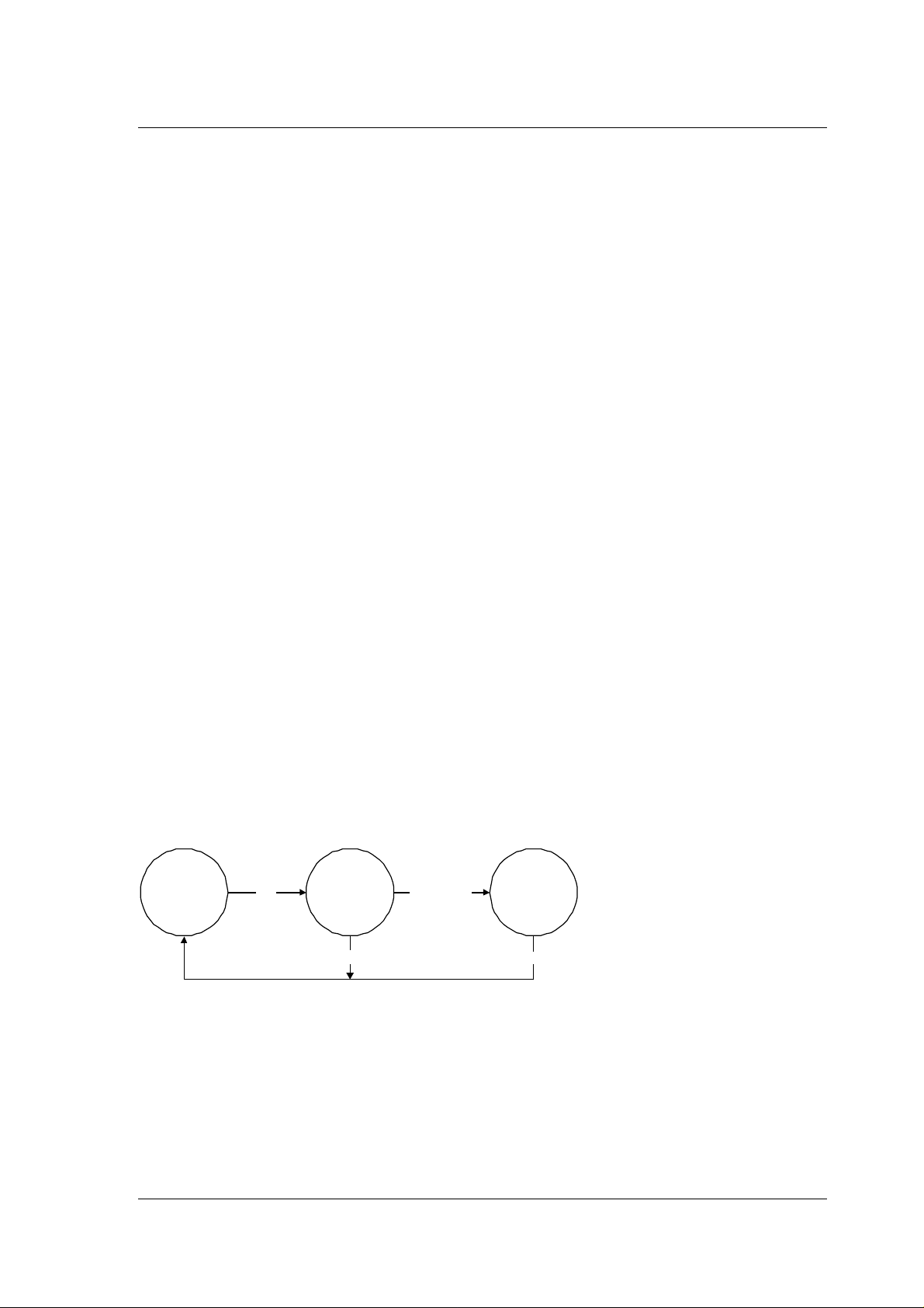
5.2 RF Link initialization
Link-locate Synchronization IdleLink Synchronized
Link -lost Link-lost
Figure 5-1 : link initialisation algorithm
5.2.1 Idle state
The nRF24Z1 link initialsation algorithm will be in its idle state when a link is established,
and the channel hopping engine is initiated and synchronized.
Page 19

PRELIMINARY PRODUCT SPECIFICATION
SUNSTAR单片机专用电路 http://www.icasic.com/ TEL: 0755-83387030 FAX:0755-83376182 E-MAIL:szss20@163.com
SUNSTAR半导体集成电路 http://www.icasic.com/ TEL: 0755-83387016 FAX:0755-83376182 E-MAIL:szss20@163.com
nRF24Z1 wireless audio streamer
5.2.2 Link-locate state
When the link between ATX and ARX is broken, a special link-locate routine is initiated
on both sides to establish a new link, see Figure 5-1. During initialization nRF24Z1
derives a set of channels from register CHP1, CHP2 and CHP3, which will be used during
channel hopping in idle state. These channels are also utilized by the link-locate routine
when acquiring a feasible startup channel for the new link.
- Link-locate on ATX
ATX tries to establish a link with ARX by iteratively sending short search packages on all
available channels until acknowledge is received from ARX. ATX will send one package
on each channel and wait for acknowledge for a specific time which is long enough to
secure that ARX has time to respond. The accumulated time used by ATX while looping
through all available channels is here defined as the ATX-loop-time. After receiving an
acknowledge package from ARX, ATX will enter the synchronization state as described in
Figure 5-1.
- Link-locate on ARX
ARX tries to establish a link with ATX by listening for incoming search packages on all
available channels until such is received. When a search package is received, ARX will
proceed by sending one acknowledge package to confirm a feasible link. ARX will listen
for incoming search packages on each channel for a fixed time which is larger than the
ATX-loop-time, which will guarantee at least one search package to get through on each
available channel used by ARX, as long as this channel is not being occupied by another
radio device. After sending the acknowledge package, ARX will enter the synchronization
state.
5.2.3 Synchronization state
This state takes care of synchronizing the channel hopping engine on ATX and ARX, to
secure that both parts follows the same hopping sequence. ATX takes initiative for starting
the channel hopping engine, by sending a start condition to ARX about when to start
hopping. Which channel to start from is implicitly found during the link-locate state.
5.3 Audio streaming
The audio data fed to the audio interfaces on a nRF24Z1 in ATX mode can be of a number
of common digital audio stream formats :
I2S (audio serial) interface:
• left justified, I2S and right justified
S/PDIF interface:
• Consumer Linear PCM Audio described in IEC 60958-3. nRF24Z1 has a single
ended CMOS interface, so to fulfil the electrical requirements external adaptation
circuitry is needed.
Page 20

PRELIMINARY PRODUCT SPECIFICATION
SUNSTAR单片机专用电路 http://www.icasic.com/ TEL: 0755-83387030 FAX:0755-83376182 E-MAIL:szss20@163.com
SUNSTAR半导体集成电路 http://www.icasic.com/ TEL: 0755-83387016 FAX:0755-83376182 E-MAIL:szss20@163.com
nRF24Z1 wireless audio streamer
• Non-Linear PCM Audio. As described in IEC 61937-1 (General) and IEC 61937-2
(Burst-info). The nRF24Z1 is transparent to the specific audio compression
algorithms used, so it covers all the described formats in IEC 61937-3 to 61937-7.
In ATX the audio stream formats are converted to the nRF24Z1 RF protocol and
transferred over the air.
In the ARX the data are validated and converted back to audio stream format and fed to the
corresponding audio output interface.
5.4 Audio receiver clock rate recovery
In all RF systems streaming ‘true time’ data, maintaining equal datarates on both sides of
RF link, is a big challenge. In other words; keeping the master clock (MCLK) for the DAC
on the receiving side, equal to the clock used to feed data into the RF device on the
transmitter side.
If these two clocks are not equal the receiving end will either run out of samples for the
DAC or overflow hence need to skip some.
Usually this problem is solved by use of very thigh tolerance crystals (expensive) or
extensive digital filtering (high current consumption) only masking or interpolating the bits
missing in the stream.
nRF24Z1 solves this problem without tight tolerance crystal or extensive digital filtering.
As long as the nRF24Z1 quality of service engine is able to maintain a RF link, the ARX
(audio receiver) locks its master clock output (MCLK) to the speed the audio stream
actually is fed into the ATX on. The MCLK signal on the ARX side is hence locked to the
reference (crystal) of the device (DSP, MCU, DECODER) feeding the audio data to the
ATX and not the crystal of the nRF24Z1 devices (ATX or ARX) themselves.
One exception; if the MCLK output option is used in audio transmitter (clocking an
external ADC for instance) the crystal on the nRF24Z1 in ATX mode is the reference for
the audio speed on the entire nRF24Z1 link.
This offers the end application a true loss less audio channel.
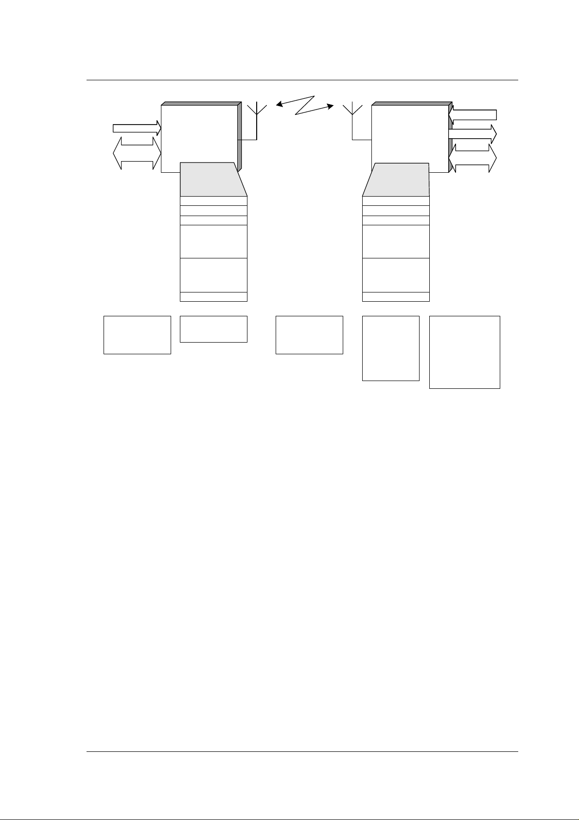
5.5 Data link
There is a 2-way, low bit rate, robust, control and data link running in parallel with the
audio stream. This data link is a part of the quality of service overhead, i.e. difference
between on the air data rate (4 MBit/s) and audio data rate 1.5 MBit/s. Data link rate can
hence not be traded for higher audio data rate. The functionality of the control and data link
is illustrated in Figure 5-2.
Page 21
PRELIMINARY PRODUCT SPECIFICATION
SUNSTAR单片机专用电路 http://www.icasic.com/ TEL: 0755-83387030 FAX:0755-83376182 E-MAIL:szss20@163.com
SUNSTAR半导体集成电路 http://www.icasic.com/ TEL: 0755-83387016 FAX:0755-83376182 E-MAIL:szss20@163.com
nRF24Z1 wireless audio streamer
DD[2:0]
SPI / 2-wire
slave
nRF24Z1
ATX mode
nRF24Z1
ARX mode
DI[3:0]
DO[3:0]
SPI / 2-wire
master
1: Data for the ARX are
fed to the ATX via
general purpose inputs or
one of the serial slave
interfaces
RXDCMD
RXWCNT
RXRCNT
RXWBUF
RXRBUF
RXEXEC
2: The ATX serial slave
interfaces gives access
to all ATX registers.
3: A sub set of the ATX
registers and the input
pin status are transferred
by RF between two
linked nRF24Z1
RXDCMD
RXWCNT
RXRCNT
RXWBUF
RXRBUF
RXEXEC
4: Resulting in a
mirror of these ATX
registers on the ARX
side. The mirrored
registers access all
ARX RF and audio
config plus digital I/O
controls and I/O
data.
5: Command register
contents (like in RXDCMD)
dictates the actions to take
place on the ARX GPIO
pins and serial master
interfaces.
Input status of general
purpose input pins (DI[3:0])
are similarly fed back to
ATX.
Figure 5-2 nRF24Z1 control and data link
Through the control and data link the ATX has full control over all registers related to ARX
configuration and can access ARX GPIO (for LED’s etc.) and the ARX 2-wire and SPI
master interface for configuring of DAC’s, volume control and other peripheral functions.
5.6 Power down mode
nRF24Z1 has a power saving mode called “Power down”. In this mode, the quality of
service engine is shut down, and only a low frequency oscillator and some timers are
running. The power down mode can be left upon sleep timer time out or on external pin
event. The ATX and ARX will now go up and start the link initialization routine as
described in section 5.2. The sleep timers also enable the nRF24Z1 to shut down again if
no counterpart is found on the air or no audio input is detected. ARX may also be put in
and out of power down mode by toggling a pin.
Page 22

PRELIMINARY PRODUCT SPECIFICATION
SUNSTAR单片机专用电路 http://www.icasic.com/ TEL: 0755-83387030 FAX:0755-83376182 E-MAIL:szss20@163.com
SUNSTAR半导体集成电路 http://www.icasic.com/ TEL: 0755-83387016 FAX:0755-83376182 E-MAIL:szss20@163.com
nRF24Z1 wireless audio streamer
6 NRF24Z1 REGISTER MAP
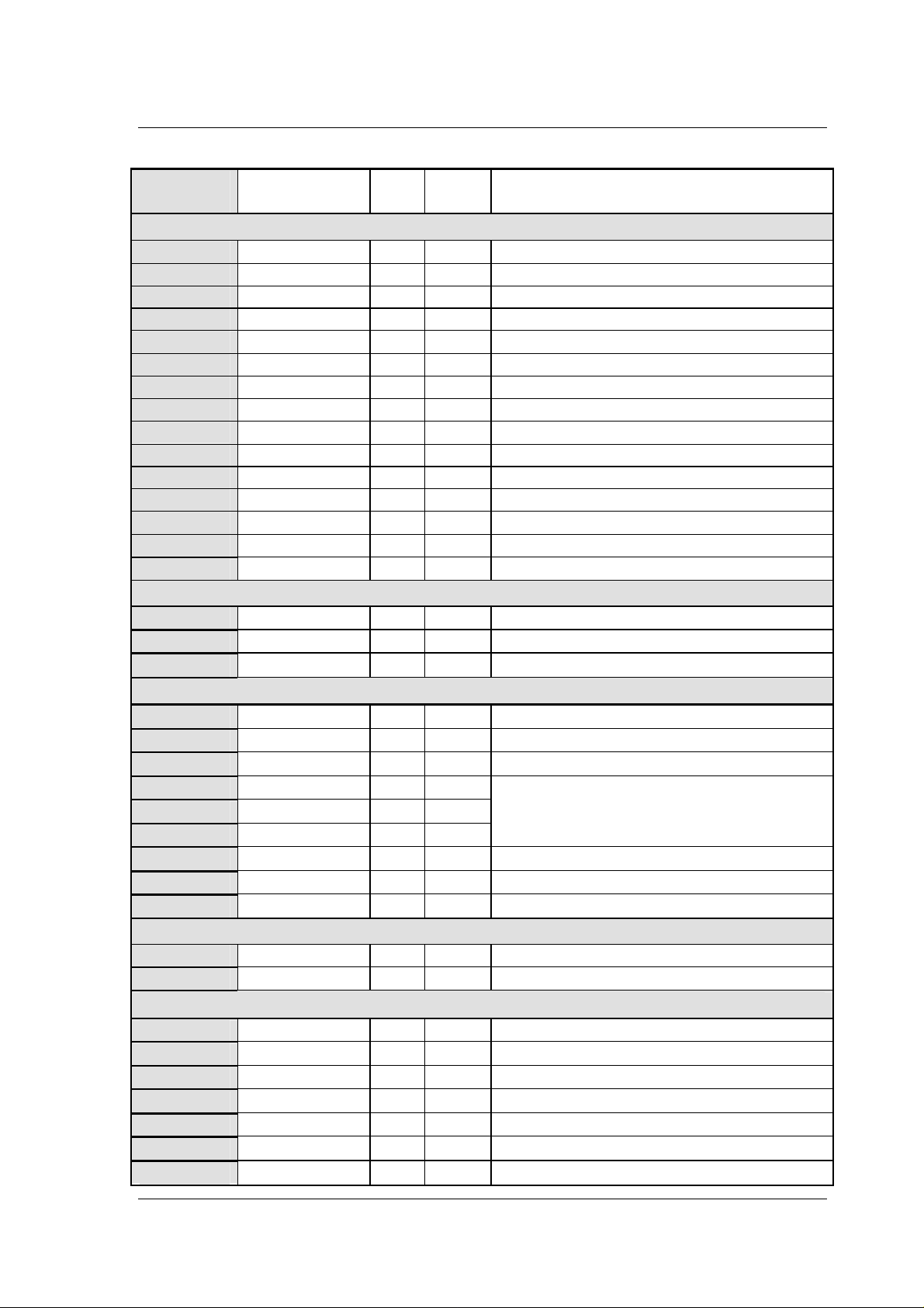
nRF24Z1 contains several control and status registers, which are listed in the table below.
The registers may be accessed by an external MCU via the (SPI or 2-wire) slave interface.
The registers are organized functinally into 6 groups; ATX , Link and ARX control and
tatus, and Data link. All registers are present both in audio transmitter and audio receiver.
The intial value of all registers is read from EEPROM (if present) immediately after reset,
othervise the initial values in Table 6-1 applies.
6.1 Access from audio transmitter side
If a MCU on the audio transmitter side writes to a register, the audio transmitter version of
the register is written, and registers TXCSTATE, LNKCSTATE, RXCSTAT, RXEXEC
controls whether also the audio receiver version of the register is written via the data link.
• If it is a ATX control register, register TXCSTATE controls if also the audio
receiver version of the register is written via the data link
• If it is a Link control register, register LNKCSTATE controls if also the
audio receiver version of the register is written via the data link
• If it is a ARX control register, register RXCSTATE controls if also the
audio receiver version of the register is written via the data link
See ch. 12 for details about how control registers are updated via the data link, and Table
7-10 about data link registers.
A MCU on the audio transmitter side can read all registers on its side, plus the Link status,
ARX status and data link registers, which are read from audio receiver via the data link.
6.2 Access from audio receiver side
If a MCU on the audio receiver side writes to a register, only the audio receiver version of
the register is written, and it is not sent via the data link to the audio transmitter. Which
implies that a MCU on audio transmitter will not know about it, but as mentioned above,
ATX MCU may read status registers via the link anytime. A MCU on the audio receiver
side can read all registers on its side, but it cannot read anything via the link. In brief ARX
MCU only has local access, while ATX MCU controls the data link.
Page 23
PRELIMINARY PRODUCT SPECIFICATION
SUNSTAR单片机专用电路 http://www.icasic.com/ TEL: 0755-83387030 FAX:0755-83376182 E-MAIL:szss20@163.com
SUNSTAR半导体集成电路 http://www.icasic.com/ TEL: 0755-83387016 FAX:0755-83376182 E-MAIL:szss20@163.com
nRF24Z1 wireless audio streamer
Address
Hex
Register R/W Initial
Hex
Description
ATX registers
0x01 TXSTA R 0x40 Table 7-4, page 28
0x20 TXDD R 0x00 Table 7-15, page 40
0x02 INTSTA R 0x00 Table 9-1, page 54
0x1A TXMOD R/W 0x01 Table 7-6, page 29
0x11 TXFMT R/W 0x00 Table 7-5, page 28
0x12 TXLAT R/W 0x00 Table 8-6, page 53
0x13 INTCF R/W 0x00 Table 9-1, page 54
0x14 I2SCNF_IN R/W 0x00 Table 7-6, page 29
0x15 I2SRAT R/W 0x00 Table 7-7, page 30
0x16 TXPWR R/W 0x03 page 53
0x17 TXSTI[0] R/W 0x00 page 58
0x18 TXSTI[1] R/W 0x00 page 58
0x19 TXWTI R/W 0x00 page 58
0x10 TXRESO R/W 0x00 page 55
0x1B TXCSTATE R/W 0x00 page 60
LINK status registers
0x03 LNKSTA R 0x00 page 52
0x04 LNKQ R 0x00 page 51
0x05 LNKERR R 0x00 page 51
LINK control registers
0x30 LNKMOD R/W 0x00 page 52
0x31 LNKWTH R/W 0xff page 51
0x32 LNKETH R/W 0xff page 51
0x35 CHP1 R/W 0x01
0x36 CHP2 R/W 0x12
0x37 CHP3 R/W 0x05
0x38 ALEN R/W 0x05 page 48
0x39 -0x3D ADDR[0:4] R/W 0x01 page 49
0x3E LNKCSTATE R/W 0x00 page 60
page 49
ARX status registers
0x06 RXSTA R 0x00 page 42
0x07 RXPIN R 0x00 Table 7-22, page 45
ARX control registers
0x4A RXMOD R/W 0x00 Table 7-8, page 31
0x41 RXPIO R/W 0x00 Table 7-20, page 44
0x42 RXPWME R/W 0x00 Table 7-21, page 44
0x43 RXPWMD R/W 0x00 Table 7-21, page 44
0x44 I2SCNF_OUT R/W 0x00 Table 7-8, page 31
0x45 RXWAKE R/W 0x28 page 57
0x49 RXPWR R/W 0x00 page 53
Page 24

PRELIMINARY PRODUCT SPECIFICATION
SUNSTAR单片机专用电路 http://www.icasic.com/ TEL: 0755-83387030 FAX:0755-83376182 E-MAIL:szss20@163.com
SUNSTAR半导体集成电路 http://www.icasic.com/ TEL: 0755-83387016 FAX:0755-83376182 E-MAIL:szss20@163.com
nRF24Z1 wireless audio streamer
0x46 RXSTI[0] R/W 0x00 page 58
0x47 RXSTI[1] R/W 0x00 page 58
0x48 RXWTI R/W 0x00 page 58
0x40 RXRESO R/W 0x00 page 55
0x4B RXCSTATE R/W 0x00 page 60
Data link registers
0x70 RXDCMD R/W 0x82 Table 7-10, page 34
0x71 RXWCNT R/W 0x00
0x72 RXRCNT R/W 0x00
0x50-0x5f RXWBUF W 0x00
0x60-0x6f RXRBUF R 0x00
0x74 RXEXEC W/R 0x00
Table 6-1 nRF24Z1 register listing
In the following chapters, the nRF24Z1 registers are described sorted by function.
Table 7-11, page 35
Page 25

PRELIMINARY PRODUCT SPECIFICATION
SUNSTAR单片机专用电路 http://www.icasic.com/ TEL: 0755-83387030 FAX:0755-83376182 E-MAIL:szss20@163.com
SUNSTAR半导体集成电路 http://www.icasic.com/ TEL: 0755-83387016 FAX:0755-83376182 E-MAIL:szss20@163.com
nRF24Z1 wireless audio streamer
7 DIGITAL I/O
This section describes the digital I/O pins, control registers and important interface timing
of the nRF24Z1.
The digital I/O pins of the nRF24Z1 are divided into three groups:
1. Audio interfaces
2. Serial master interfaces
3. Control and GPIO interfaces
7.1 Digital I/O behaviour during RESET
During reset all digital pins, except the master SPI interface output pins, are set as inputs to
avoid driving conflicts. The master SPI pins MCSN, MSCK and MMOSI are set to output
high, that is, in inactive SPI state, ready to read EEPROM configuration data, which is the
first thing to happen after reset. All pins will remain in their respective direction until one
of the configuration read routines described in section 5.1 is finished, and thereafter I/O
pins are set according to new configuration data.
7.2 Audio interfaces
The audio interface group are defined as the I2S and S/PDIF interfaces plus the MCLK and
REQ pins.
Pin name Function
CLK bit clock
WS word sync clock
DATA audio data
MCLK 256 * audio fundamental sample rate output, see Table 7-4 .
REQ data request, used for burst type data, see Table 7-7.
SPDIO S/PDIF serial in- or output, see ch. 7.4.
Table 7-1 serial audio port pins
7.3 I2S Audio Interface
nRF24Z1 has a three-wire serial audio port which can be configured to be compatible with
different serial audio formats. In ATX mode, the audio port is in slave (receive) mode. In
ARX mode, the audio port is in master (transmit) mode. The audio port consists altogether
of 6 pins, see Table 7-1.
Page 26

PRELIMINARY PRODUCT SPECIFICATION
SUNSTAR单片机专用电路 http://www.icasic.com/ TEL: 0755-83387030 FAX:0755-83376182 E-MAIL:szss20@163.com
SUNSTAR半导体集成电路 http://www.icasic.com/ TEL: 0755-83387016 FAX:0755-83376182 E-MAIL:szss20@163.com
nRF24Z1 wireless audio streamer
Figure 7-1 : some serial audio formats
audio format I2SCNF[3:0] value
Left justified 0xA
I2S 0x0
Right Justified 0xB
Table 7-2 : Example of I2SCNF setting for some common serial audio formats , applies to
both I2SCNF_IN and I2SCNF_OUT registers.
See also Table 7-7 and Table 7-8.
7.4 S/PDIF Audio Interface
nRF24Z1 supports the following formats of the S/PDIF interface:
• Consumer Linear PCM Audio described in IEC 60958-3. nRF24Z1 has a single
ended CMOS interface, so to fulfil the electrical requirements external adaptation
circuitry is needed.
• Non-Linear PCM Audio, as described in IEC 61937-1 (General) and IEC 61937-2
(Burst-info). nRF24Z1 is transparent to the specific audio compression algorithms
used, it just transfers what comes in on the input side to the receiver side. Except
that only the 32 first bits of channel status information bits are transferred, and no
user data bits.
Page 27

PRELIMINARY PRODUCT SPECIFICATION
SUNSTAR单片机专用电路 http://www.icasic.com/ TEL: 0755-83387030 FAX:0755-83376182 E-MAIL:szss20@163.com
SUNSTAR半导体集成电路 http://www.icasic.com/ TEL: 0755-83387016 FAX:0755-83376182 E-MAIL:szss20@163.com
nRF24Z1 wireless audio streamer
Only one of the audio interfaces can be active at one time. The active audio interface for
ATX is chosen by bit 2 in register TXMOD (0= I2S is default, see Table 7-16), and for
ARX by bit 2 in register RXMOD.
7.5 Audio interface functionality
The functionality and direction of the pins in the audio interfaces are listed in Table 7-3.
MODE=0 (ARX) MODE =1 (ATX) nRF24Z1 Audio
interfaces
Pin # Pin
name
9 REQ REQ IN X IN REQ OUT X OUT
10 CLK CLK OUT X IN CLK IN X IN
11 WS WS OUT X IN WS IN X IN
12 DATA DATA OUT X IN DATA IN X IN
13 SPDIO
14 MCLK MCLK OUT X OUT MCLK OUT X OUT
TXMOD[2]=0
(I2S)
Function Direction Function Direction Function Direction Function Direction
X IN X IN
RESET* OUT
TXMOD[2]=1
(S/PDIF)
SPDIO OUT
TXMOD[2]=0
(I2S)
RESET* OUT
TXMOD[2]=1
(S/PDIF)
SPDIO IN
Table 7-3 Audio interface pin functions
* If S/PDIF is not used for audio, the SPDIO pin can be used as RESET (output) to external devices. Please see chapter 10 for further
details.
7.5.1 ATX audio interface control
The nRF24Z1 in ATX mode automatically detects the rate of a digital audio stream from an
external master both on the I2S and S/PDIF interface. Register 0x01 holds the status of this
detection for optional read back to an external MCU.
Page 28

PRELIMINARY PRODUCT SPECIFICATION
SUNSTAR单片机专用电路 http://www.icasic.com/ TEL: 0755-83387030 FAX:0755-83376182 E-MAIL:szss20@163.com
SUNSTAR半导体集成电路 http://www.icasic.com/ TEL: 0755-83387016 FAX:0755-83376182 E-MAIL:szss20@163.com
nRF24Z1 wireless audio streamer
Address
Hex
Register R/W Initial
Hex
Description
0x01 TXSTA R 0x40 Audio transmitter status register
Bit Interpretation
7 Reserved
6:5
Detected audio scale factor (I2S only)
00 0.25
01 0.5
10 1
11 2 1
4:3
Detected audio fundamental rate
00 48 kHz
01 44.1 kHz
10 32 kHz
11 Illegal or no input detected
2:0 Audio transmitter state (TBD)
Table 7-4 Audio input status
Default nRF24Z1 transfers uncompressed audio, but it has some options to transfer
companded audio data. This can be used to save power, or to accommodate transfer of 24
bit audio, which uncompanded would exceed the radio bandwidth. This is a lossy
compression/decompresion in the way that superfluous LSB's are lost. Here is an example
of how 24 to 16 bit compand works:
If the sample values within an audio frame are within +/- 200000, 3 LSB are cut, and if
sample values of the next frame is within +/- 60000, only 1 LSB is lost. So the number of
LSB lost varies dynamically with maximum sample value for each frame, and this limits
the relative error.
Address
Hex
Register R/W Initial
Hex
Description
0x11 TXFMT R/W 0x00 Transmit data format
Value Interpretation
0 16 bit linear PCM
1 24 bit linear companded to 16 bit
2 Reserved
4 16 bit linear companded to 8 bit
Table 7-5 : register TXFMT.
1
For 2x rate (96 kHz) every second sample is discarded in ATX, and in ARX the remaining samples are
output at 1x rate.
Page 29

PRELIMINARY PRODUCT SPECIFICATION
SUNSTAR单片机专用电路 http://www.icasic.com/ TEL: 0755-83387030 FAX:0755-83376182 E-MAIL:szss20@163.com
SUNSTAR半导体集成电路 http://www.icasic.com/ TEL: 0755-83387016 FAX:0755-83376182 E-MAIL:szss20@163.com
nRF24Z1 wireless audio streamer
The Audio interfaces in ATX mode are controlled by registers 0x1A (Bit[4], Bit[2:0]) and
0X14 listed in Table 7-5.
Address
Hex
0x1A TXMOD R/W 0x00 Operation modes for audio transmitter
0x14 I2SCNF_IN R/W 0x00 I2S interface configuration (on ATX side), see
Table 7-6 ATX audio input control
Register R/W Initial
Hex
Description
7 RF transmitter enable
6 Audio transmitter power down
5 Enable wakeup on changing DD[1]
4 REQ pin polarity (0 for active low)
3 Enable direct data from pins
DD[2:0].
DD[2] is only available if SSEL=1
2 S/PDIF enable (default input is I2S)
1:0
MCLK output control**
00 MCLK off (logic 0)
01 Output 256 x 48 kHz
10 Output 256 x 44.1 kHz
11 Output 256 x 32 kHz
also Table 7-2
7 Data enable
0 I2S carries sound
1 I2S carries data
6 Reserved, MBZ
3 WS Polarity
0 WS=0: Left sample (std)
1 WS=1: Left sample
2 Data to Bit Clock relation
(data valid at clock edge)
0 Rising Edge (standard)
1 Illegal
1 WS to MSB delay
0 1 clock cycle (standard)
1 0 clock cycles
0 Audio word justification
0 Left justified
1 Right justified
**IMPORTANT NOTE!
For S/PDIF audio input, MCLK output is disabled, but the MCLK control value TXMOD[1:0] should
generally be set to the expected sampling rate. This is mandatory if 32 kHz sampling rate is expected, and
recommended otherwise. Setting MCLK to the expected sampling rate gives the best phase margin and hence
sampling quality when the input S/PDIF signal has much jitter.
Page 30

PRELIMINARY PRODUCT SPECIFICATION
SUNSTAR单片机专用电路 http://www.icasic.com/ TEL: 0755-83387030 FAX:0755-83376182 E-MAIL:szss20@163.com
SUNSTAR半导体集成电路 http://www.icasic.com/ TEL: 0755-83387016 FAX:0755-83376182 E-MAIL:szss20@163.com
nRF24Z1 wireless audio streamer
To pace I2S data a REQ output signal is used. Polarity is set in TXMOD[4]. In I2S data
mode (I2SCNF_IN7=1) I2S DATA and CLK input must be stopped within 32 CLK cycles
when REQ goes inactive, and must start again when REQ goes active.
For analog audio sources, the nRF24Z1 offers a 256x clock output on pin MCLK
(TXMOD[1:0]). This clock can be used as system clock for an external stereo ADC.
If I2S is used for data transfers (I2SCNF_IN[7] = 1), average data rate is set in register
0x15
Address
Hex
0x15 I2SRAT R/W 0x00 I2S interface speed for digital input streams that
Register R/W Initial
Hex
Description
are not interpreted as audio by nRF24Z1.
n (dec) Digital stream
0 8 kbit/s
1 16 kbit/s
2-190 (n+1)*8 kbit/s
191 1536kbit/s
>191 Illegal
Table 7-7 ATX I2S data transfer control
7.5.2 ARX audio interface control
In ARX mode the audio interfaces are controlled by the registers 0x4A and 0x44 listed in
Table 7-8.
Page 31

PRELIMINARY PRODUCT SPECIFICATION
SUNSTAR单片机专用电路 http://www.icasic.com/ TEL: 0755-83387030 FAX:0755-83376182 E-MAIL:szss20@163.com
SUNSTAR半导体集成电路 http://www.icasic.com/ TEL: 0755-83387016 FAX:0755-83376182 E-MAIL:szss20@163.com
nRF24Z1 wireless audio streamer
Address
Hex
0x4A RXMOD R/W 0x00 Set operation modes for audio receiver
0x44 I2SCNF_OUT R/W 0x00 I2S interface configuration for audio output (on
Register R/W Initial
Hex
Description
Bit Interpretation
7 Receiver power down
6 Reserved, MBZ
5 RF receiver enable
4 REQ pin polarity
3 Reserved, MBZ
2 S/PDIF enable
1:0 Reserved, MBZ
ARX side), see also Table 7-2
Bit Interpretation
7 Reserved, MBZ
6 Mute sound output
5:4 Sample length
00 16-bit samples
01 reserved
10 24-bit samples
11 reserved
3 WS Polarity
0 WS=0: Left sample (std)
1 WS=1: Left sample
2 Data to Bit Clock relation
(data valid at clock edge)
0 Rising edge (standard)
1 Falling edge
1 WS to MSB delay
0 1 clock cycle (standard)
1 0 clock cycles
0 Audio word justification
0 Left justified
1 Right justified
Table 7-8 ARX audio interface control registers
In I2S data mode (I2SCNF_IN7=1) I2S DATA and CLK out will be stopped within 32
CLK cycles when REQ input goes inactive, and will start again when REQ goes active.
NOTE:
After reset, the ARX registers can be accessed by the audio transmitter (nRF24Z1 in
ATX mode) through the control and data channel set up between two linked
nRF24Z1.
Page 32
PRELIMINARY PRODUCT SPECIFICATION
SUNSTAR单片机专用电路 http://www.icasic.com/ TEL: 0755-83387030 FAX:0755-83376182 E-MAIL:szss20@163.com
SUNSTAR半导体集成电路 http://www.icasic.com/ TEL: 0755-83387016 FAX:0755-83376182 E-MAIL:szss20@163.com
nRF24Z1 wireless audio streamer
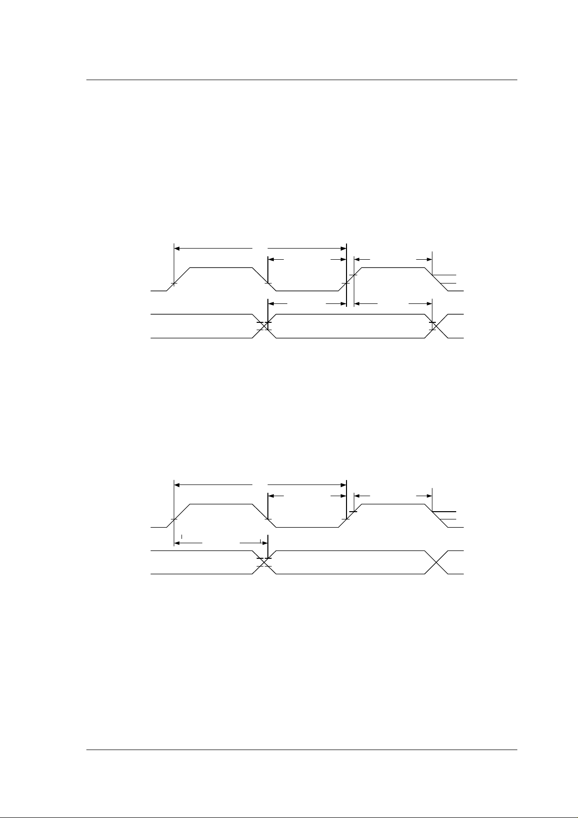
7.5.3 I2S Audio interface timing
I2S input (ATX) timing
The I2S input protocol is configurable to handle several I2S formats. In addition, the
interface will automatically detect sample size and word length for the most common
formats. This section shows the detailed bit, clock and word timing requirements.
T
I2S
CLK
DATA
and
WS
T
I2S
= clock period
t
hI2S
= hold time I2S receiver
t
sI2S
= setup time I2S receiver
Figure 7-2. Timing for I2S input on nRF24Z1, for values see Table 13-1
I2S output (ARX) timing
I2S output is protocol compatible with most I2S DACs and CODECs.
T
I2S
CLK
>= 0.35T
t
sI2S
>= 0.35T
I2S
I2S
>= 0.35T
t
hI2S
>= 0.35T
I2S
VH = 2.0V
VL = 0.8V
I2S
VH = 2.0V
VL = 0.8V
t
dI2S
DATA
and
WS
T
I2S
= clock perod
t
dI2S
= delay I2S transmitter
Figure 7-3. Timing for I2S output of nRF24Z1, for values see Table 13-1
Page 33

PRELIMINARY PRODUCT SPECIFICATION
SUNSTAR单片机专用电路 http://www.icasic.com/ TEL: 0755-83387030 FAX:0755-83376182 E-MAIL:szss20@163.com
SUNSTAR半导体集成电路 http://www.icasic.com/ TEL: 0755-83387016 FAX:0755-83376182 E-MAIL:szss20@163.com
nRF24Z1 wireless audio streamer
7.6 Serial master interfaces
The nRF24Z1 serial master interfaces group contains a SPI and a 2-wire master interface
available at all times.
After RESET the nRF24Z1 will look for a serial memory on the SPI master interface. If no
memory is present, the process is repeated on the 2-wire interface. If no memories is found
an nRF24Z1 assumes an external microcontroller will configure it over one of the slave
control interfaces and will hence be idle until that happens. Link initialization will start as
soon as the necessary control register bits are set.
During the configuration the SPI master is operated at 1MHz or 0.5MHz. SPI format is
CPOL=0, CHPA=0 as used by industry standard EEPROM/FLASH memories.
The nRF24Z1 is protocol comp atible with SPI memory with sizes ranging from 1 Kbyte to
64 Kbytes with 16-bit sub-address used.
The slave(s) that are connected determines the protocol on the 2-wire master interface. For
the case of configuration, nRF24Z1 is protocol compatible with “industry standard” 2-wire
memory with sizes ranging from 128 bytes to 4 Kbytes (with 3 address pins and one byte
sub-address used). During configuration this interface is operated at 100 kHz for
compatibility with most serial 2-wire memories.
The pin out and functionality of the serial master I/O pins are shown in Table 7-9.
ARX mode ATX mode nRF24Z1
I/O:
serial
masters
pin name
27 MSDA MSDA IN/OUT
28 MSCL MSCL OUT X IN X IN MSCL OUT
29 MSCN X IN MSCN OUT MSCN OUT X IN
30 MMISO X IN MMISO IN MMISO IN X IN
31 MMOSI
35 MSCK X IN MSCK OUT MSCK OUT X IN
MODE=0
RXDCMD[7] = 0
Functio
n Direction Function Direction Function Direction Function Direction
X IN X IN
RESET
* OUT MMOSI OUT MMOSI OUT RESET* OUT
MODE=0
RXDCMD[7] = 1
X IN X IN
RESET* OUT RESET* OUT
MODE=1
and EEPROM
connected to SPI
MODE =1
and EEPROM
connected to 2 wire
MSDA IN/OUT
Table 7-9 Serial masters functionality
* A pin in the serial interface that is NOT used for external memory and/or controlling external circuitry can be
configured to act as reset for external devices such an ADC or DAC. Please refer to chapter 10 for further details.
After configuration, the master interfaces in ATX go idle with pins still active, while the
interfaces in ARX become an extended arm of a linked ATX through the control channel
between two nRF24Z1.
The set-up of the serial master interfaces of the ARX after configuration is loaded is
controlled by register RXDCMD (0x70) as shown in Table 7-10.
Page 34

PRELIMINARY PRODUCT SPECIFICATION
SUNSTAR单片机专用电路 http://www.icasic.com/ TEL: 0755-83387030 FAX:0755-83376182 E-MAIL:szss20@163.com
SUNSTAR半导体集成电路 http://www.icasic.com/ TEL: 0755-83387016 FAX:0755-83376182 E-MAIL:szss20@163.com
nRF24Z1 wireless audio streamer
Address
Hex
0x70 RXDCMD R/W 0x82 Data “command”. Specifies interface and speed
Register R/W Initial
Hex
Description
Bit Interpretation
7 Interface select
0 Use ARX 2-wire interface
1 Use ARX SPI interface
6:4 SPI slave select control. Set which
signal to be used as slave select, and
associated polarity. Or 2-wire access
type.
Value SPI interpretation
000 CSN, active low2
001 DO[0], active low1
010 DO[1], active low1
011 DO[2], active low1
100 CSN, active low2
101 DO[0], active high1
110 DO[1], active high1
111 DO[2], active high1
Value 2-wire interpretation
000 start stop access
001 start only access (a start
only access followed by a
start-stop access will be a
start-start-stop access)
Notes:
1. In order to use any of DO[2:0] as SPI slave
selects, the corresponding bit in RXPIO
should be set to the SPI slave select
inactive state. I.e. if DO[0] is to be used as
active low slave select, RXPIO[0] must be
set to 1.
2. MCSN is always active low
3:1 Speed select
Value
(bin)
SPI
Interpretation
2-wire
Interpretation
000 8 Mbit/s Illegal
001 8 Mbit/s 100 kbit/s
010 4 Mbit/s 400 kbit/s
011 2 Mbit/s 1 Mbit/s
100 1 Mbit/s Illegal
101 500 kbit/s Illegal
110 250 kbit/s Illegal
111 Reserved Reserved
0 Reserved, MBZ.
Table 7-10 RXDCMD register
Page 35

PRELIMINARY PRODUCT SPECIFICATION
SUNSTAR单片机专用电路 http://www.icasic.com/ TEL: 0755-83387030 FAX:0755-83376182 E-MAIL:szss20@163.com
SUNSTAR半导体集成电路 http://www.icasic.com/ TEL: 0755-83387016 FAX:0755-83376182 E-MAIL:szss20@163.com
nRF24Z1 wireless audio streamer
Number of bytes data to read/write is set in ‘write and read count’ registers RXWCNT
(0x71) and RXRCNT (0x72) and the actual data are transferred through the data buffers
RXWBUF and RXRBUF. Once the above registers are set, writing to RXEXEC will
initiate a SPI or 2-wire operation on the ARX serial master interfaces. Operation finished is
also reported in RXEXEC and can be coupled to an interrupt in the ATX. See also Figure
5-2 nRF24Z1 control and data link
Remember that all interaction with these registers is done through the slave interfaces on
the ATX. The data in RXWBUF are transferred to the ARX via RF and the interactions are
carried out on the ARX side as configured in RXDCMD. Once it is completed and data
read by the ARX is transferred back to the ATX, the ‘operation finished’ interrupt (flag
INTSTA.4) is set and data read on the ARX side are available in RXRBUF.
Address
Hex
0x71 RXWCNT R/W 0x00 Number of bytes to write (max 16)
0x72 RXRCNT R/W 0x00 Number of bytes to read (max 16)
0x500x5f
0x600x6f
0x74 RXEXEC W/R 0x00 Write to this register will execute a command on
Register R/W Initial
Hex
Description
RXWBUF W 0x00 Data to be written to the interface specified by
RXDCMD
RXRBUF R 0x00 Data read from audio receiver on the interface
specified by RXDCMD
the audio receiver. The interface and speed are
specified by RXDCMD. The audio receiver will
first write RXWCNT bytes from RXWBUF to
the selected interface, then read RXRCNT bytes
and transmit back to be stored in RXRBUF. An
interrupt may be delivered upon successful
completion of the command.
0= idle; 1=write or read
MCU must set RXEXEC=1 to perform
command, and can thereafter read RXEXEC to
find if command is finished (idle)
Table 7-11 ARX master data registers
Page 36

PRELIMINARY PRODUCT SPECIFICATION
1-789
1-789
8
9
SUNSTAR单片机专用电路 http://www.icasic.com/ TEL: 0755-83387030 FAX:0755-83376182 E-MAIL:szss20@163.com
SUNSTAR半导体集成电路 http://www.icasic.com/ TEL: 0755-83387016 FAX:0755-83376182 E-MAIL:szss20@163.com
nRF24Z1 wireless audio streamer
7.6.1 Timing serial master interfaces
SPI master timing
t
MCSN
MSCK
MMOSI
dMSCK
t
dMSPI
MSB LSB
T
MSCK
t
hdMSPI
MMISO
t
suMSPI
MSB LSB
Figure 7-4 : SPI master interface timing, here is shown a one byte transaction.
T
t
t
: MSCK cycle time, as defined by RXDCMD register.
MSCK
: time from MCSN active to first SCK pulse, t
dMSCK
: delay from negedge MSCK to new MMOSI output data
dMSPI
t
: MMISO setup time to posedge MSCK.
suMSPI
t
: MMISO hold time to posedge MSCK.
hdMSPI
dSCK
= T
MSCK
/ 2
for values see Table 13-1
2-wire master timing
START
Condition
SDA
STOP
Condition
SCL
ADDRESS
ACK DATA ACK DATA ACK
R/W
1-7
Figure 7-5 : 2-wire data transfer
Page 37

PRELIMINARY PRODUCT SPECIFICATION
T
SUNSTAR单片机专用电路 http://www.icasic.com/ TEL: 0755-83387030 FAX:0755-83376182 E-MAIL:szss20@163.com
SUNSTAR半导体集成电路 http://www.icasic.com/ TEL: 0755-83387016 FAX:0755-83376182 E-MAIL:szss20@163.com
nRF24Z1 wireless audio streamer
MSCL
MSCL
MSDA out
MSDA in
t
MW2_od
t
MW2_dsu
t
MW2_od
t
MW2_dhd
Figure 7-6 : 2-wire master timing, for values see Table 13-1
7.7 Control and GPIO interfaces
The following control and GPIO interfaces are found:
• ATX: SPI or 2-wire slave interfaces and general purpose inputs(DD [2:0])
• ARX: SPI or 2-wire slave interfaces as for ATX, or GPIO pins DI[3:0],
DO[3:0] with alternative functionality: PWM or master SPI chip select
signals
The ATX serial slave interfaces are the main channel for external applications or devices to
control the nRF24Z1 and the RF communication. All register access and all but the most
basic control and data transfers’ takes place through one of these interfaces.
If an external controlling device (microcontroller) is not present in the audio transmitter
(ATX), nRF24Z1 configuration can only be done once directly after RESET (section 7.6).
All audio and RF link set-up is fixed and the data/control channel offered can only carry
simple button push/interrupt signals.
7.7.1 ATX control and GPIO pins
In ATX mode the pins are mainly carrying the serial slave control interfaces that enables
access and control of all the nRF24Z1 registers both in the device physically connected and
a linked ARX (through the nRF24Z1 data/control RF channel).
One of two interfaces can be chosen based on the level of input pin SSEL.
SSEL = 0; SPI (pins SCSN, SSCK, SMISO, SMOSI).
SSEL = 1; 2-wire (pins SADR, SSCL and SSDA)
The functionality and signal direction of the pins in ATX mode are listed in the table
below.
Page 38

PRELIMINARY PRODUCT SPECIFICATION
SUNSTAR单片机专用电路 http://www.icasic.com/ TEL: 0755-83387030 FAX:0755-83376182 E-MAIL:szss20@163.com
SUNSTAR半导体集成电路 http://www.icasic.com/ TEL: 0755-83387016 FAX:0755-83376182 E-MAIL:szss20@163.com
nRF24Z1 wireless audio streamer
nRF24Z1 GPIO and
serial slave interface
pins
Device control: SPI
MODE, SSEL = 10
ATX mode
Device control:
2-wire
MODE, SSEL =11
pin name
Function Direction Function Direction
1 SSEL SSEL IN SSEL IN
2 SMISO/SSDA SMISO OUT SSDA IN/OUT
3 SSCK/SSCL SSCK IN SSCL IN/OUT
4 SCSN/SADR SCSN IN SADR IN
6 SMOSI/DD[2] SMOSI IN DD[2] IN
7 DD[1] DD[1] IN DD[1] IN
8 DD[0] DD[0] IN DD[0] IN
26 MODE MODE IN MODE IN
36 IRQ IRQ OUT IRQ OUT
Table 7-12 ATX Control and GPIO pins functionality
7.7.2 SPI slave interface
The first byte of the SPI transaction is a special command which specifies the register
address and whether it is a read or a write access. The seven least significant bits in the first
byte is the nRF24Z1 register address, while the most significant bit is the read/write
indicator (read=1,write=0), see Table 7-13
B7 B6 B5 B4 B3 B2 B1 B0
R/W
Register address
Table 7-13 SPI command byte encoding
Write transaction : The next byte on SMOSI will be put into register with address as set in
the first byte. Writing more bytes will autoincrement the register address.
Read transaction : The next byte on SMISO will be value of register with address as set in
first byte. Reading more bytes will autoincrement the register address.
Consecutive accesses with SCSN low will auto-increment the address. This means that all
registers may theoretically be accessed with one SPI transfer.
7.7.3 2-wire slave interface
This interface is similar to what is found on serial memories and data converter devices.
The 7-bit device address of nRF24Z1 is ‘a101001’, where ‘a’ is the logic level of the
SADR input pin (read during power up and reset only).
Each 2-wire transaction is started with the “Start condition” followed by the first byte
which contains the 7 bit long device address and one read/write bit, this byte is hereafter
referred to as the “address/read command byte” or the “address/write command byte”
depending on the state of the read/write bit, read=1, write=0. The second byte contains the
Page 39

PRELIMINARY PRODUCT SPECIFICATION
SUNSTAR单片机专用电路 http://www.icasic.com/ TEL: 0755-83387030 FAX:0755-83376182 E-MAIL:szss20@163.com
SUNSTAR半导体集成电路 http://www.icasic.com/ TEL: 0755-83387016 FAX:0755-83376182 E-MAIL:szss20@163.com
nRF24Z1 wireless audio streamer
register address which specifies which nRF24Z1 register is to be accessed. This address
will be written into the ATX chip, it is therefore necessary that the first byte after the first
start condition is an address/write command. Further actions on the 2-wire interface depend
on whether the access is a read or write access. W2 command byte is illustrated in Table
7-14.
B7 B6 B5 B4 B3 B2 B1 B0
a 1 0 1 0 0 1 R/W
Table 7-14 : 2-wire command byte encoding
7.7.3.1 2-Wire write access.
Figure 7-7 illustrates a simple write operation, where one byte is written to the ATX chip.
Stop
Device Address
(7-bit)
Write ACK ACK ACKStart
Register address Data IN
Figure 7-7 : example of a 2-wire write operation
A write access is composed by a start condition, an address/write command byte, a register
address byte and a data byte which will be written to the register specified in the previous
register address byte. Each byte will be acknowledged by the 2-wire slave by pulling the
data line (SDA) low. To stop the write access a stop condition should be applied on the 2wire interface. See Figure 7-9 for an example. Consecutive write access is performed by
postponing the stop condition.
7.7.3.2 2-Wire read access
Figure 7-8 illustrates a simple read operation, where one byte is read back from the ATX
chip.
NACK
Device Address
(7-bit)
Start Stop
Write ACK ACK
Register address Data IN
Device Address
(7-bit)
Start (repeated)
Read ACK
Figure 7-8 : example of a 2-wire read operation
A read access is composed by a start condition, an address/write command byte, and a
register address byte. These two bytes are acknowledged by the 2-wire slave. This scenario
is followed by a repeated start condition and an address/read control byte. This byte is also
Page 40

PRELIMINARY PRODUCT SPECIFICATION
SUNSTAR单片机专用电路 http://www.icasic.com/ TEL: 0755-83387030 FAX:0755-83376182 E-MAIL:szss20@163.com
SUNSTAR半导体集成电路 http://www.icasic.com/ TEL: 0755-83387016 FAX:0755-83376182 E-MAIL:szss20@163.com
nRF24Z1 wireless audio streamer
acknowledged by the 2-wire slave. After the acknowledge bit has been sent from the 2-wire
slave, the register value which corresponds to the register address byte will be supplied by
the 2-wire slave as well. This byte should be acknowledged by the 2-wire master if
consecutive register read is wanted. The read access is stopped by not acknowledging the
last byte read, followed by a stop condition. See Figure 7-9 for an example.
Start
condition
1 18 9 8 9
condition
Stop
D7 D0 ACK D7 D0
ACK/NACK
Figure 7-9 : example of 2-wire waveform
7.7.4 General purpose input pins D[2:0]
Three (2 if SPI slave is used, SSEL=0) general purpose inputs are also available. The status
on these pins can be read in register 0x20
Address
Hex
Register R/W Initial
Hex
Description
0x20 TXDD R 0x00 Value of ATX DD input pins
Bit Interpretation
7:3 Reserved, do not use
2 Value of DD2 (only if SSEL=1)
1 Value of DD1
0 Value of DD0
Table 7-15 ATX DD[2:0] status
If bit TXMOD[3] is set the levels of pins DD[2:0] are mirrored on pins DO[2:0] on a linked
ARX device directly. See Table 7-16
Address
Hex
Register R/W Initial
Hex
Description
0x1A TXMOD R/W 0x00 Operation modes for audio transmitter
7 RF transmitter enable
6 Audio transmitter power down
5 Enable wakeup on changing DD[1]
4 REQ pin polarity
3 Enable direct data from pins
DD[2:0].
DD[2] is only available if SSEL=1
2 S/PDIF enable
1:0 MCLK output control
Table 7-16 TXMOD register
Page 41

PRELIMINARY PRODUCT SPECIFICATION
SUNSTAR单片机专用电路 http://www.icasic.com/ TEL: 0755-83387030 FAX:0755-83376182 E-MAIL:szss20@163.com
SUNSTAR半导体集成电路 http://www.icasic.com/ TEL: 0755-83387016 FAX:0755-83376182 E-MAIL:szss20@163.com
nRF24Z1 wireless audio streamer
The IRQ pin can act as an interrupt signal to the outside application. There are a number of
interrupt sources available; this is described further in chapter 9.
7.7.5 ATX Control interface timing
7.7.5.1 SPI slave timing
The SPI slave can operate with up to 8 MHz clock speed over the full operation range of
the device. With a 3V +/-10% supply the maximum clock speed is 16MHz. However note
that there is a minimum pause interval t
t
dSSCK
SCSN
T
SSCK
between writing or reading a each byte.
SRD
t
SRD
SSCK
t
dSSPI
SMISO
SMOSI
MSB
MSB
t
suSSPI
Figure 7-10 : SPI slave timing diagram
T
: SSCK cycle time.
SSCK
t
t
: time from SCSN active to first SSCK pulse
dSSCK
t
: delay from negedge SSCK to new SMISO output data
dSSPI
: SMOSI setup time to posedge SSCK
suSSPI
t
: SMOSI hold time to posedge SSCK
hdSSPI
t
: minimum pause between each byte read from or written to slave SPI
SRD
for values see Table 13-1
t
hdSSPI
LSB
LSB
MSB
next byte
MSB
next byte
7.7.5.2 2-wire slave timing
The interface supports 100 kHz, 400 kHz and 1MHz over the operating range of the device.
Page 42

PRELIMINARY PRODUCT SPECIFICATION
T
SUNSTAR单片机专用电路 http://www.icasic.com/ TEL: 0755-83387030 FAX:0755-83376182 E-MAIL:szss20@163.com
SUNSTAR半导体集成电路 http://www.icasic.com/ TEL: 0755-83387016 FAX:0755-83376182 E-MAIL:szss20@163.com
nRF24Z1 wireless audio streamer
SSCL
SSCL
SSDA in
SSDA out
t
SW2_od
t
SW2_dsu
t
SW2_dhd
t
SW2_od
Figure 7-11 : 2-wire slave timing diagram, for values see Table 13-1
7.7.6 ARX control interface options
ARX is default configured with a control slave interface, identical to ATX slave interface,
SPI or 2-wire as selected by pin SSEL, in the same way as for ATX. The slave interface
gives local access to all registers in ARX, but not to any registers on the ATX side.
Alternatively if bit 6 of RXSTA register is set in the configuration EEPROM, ARX will be
configured with GPIO pins instead of slave control interface pins. The pin out and
functionality of the slave interface or GPIO pins are shown in Table 7-18
Address
Hex
Register R/W Initial
Hex
Description
0x06 RXSTA R 0x00 ARX status register.
Bit Interpretation
7 RXEXEC status, 1 is OK, 0 is error
6 0 : ARX has control slave interface
1 : ARX has GPIO interface, which
implies no control slave interface
Table 7-17: ARX status register
Page 43
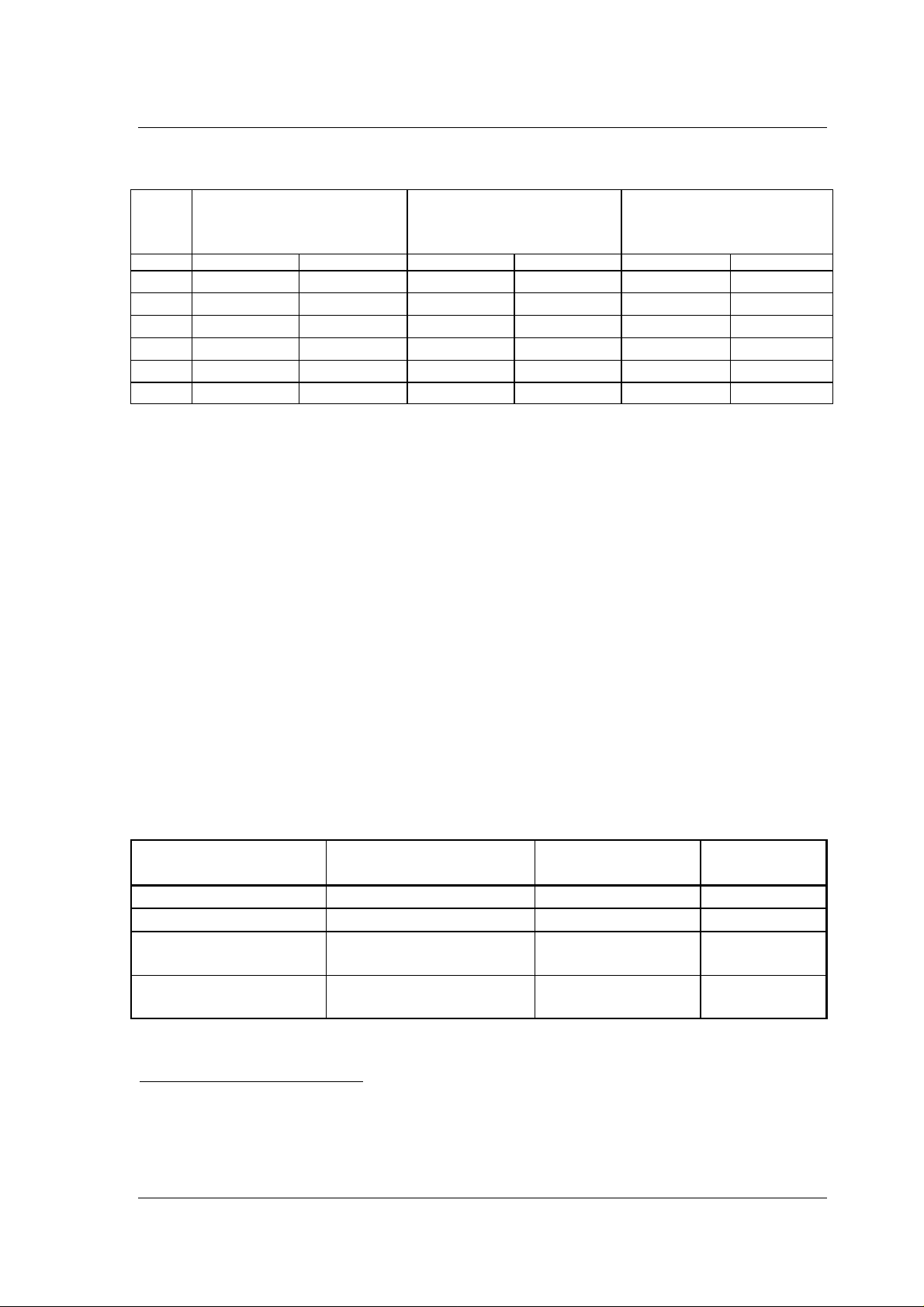
PRELIMINARY PRODUCT SPECIFICATION
SUNSTAR单片机专用电路 http://www.icasic.com/ TEL: 0755-83387030 FAX:0755-83376182 E-MAIL:szss20@163.com
SUNSTAR半导体集成电路 http://www.icasic.com/ TEL: 0755-83387016 FAX:0755-83376182 E-MAIL:szss20@163.com
nRF24Z1 wireless audio streamer
ARX with SPI
slave interface
RXSTA6 = 0, SSEL=0
Pin Function Direction Function Direction Function Direction
1 SSEL IN SSEL IN DO2 OUT
2 SMISO OUT SSDA IN/OUT DO1 OUT
3 SSCK IN SSCL IN/OUT DO0 OUT
4 SCSN IN SADR IN DI3 IN
6 SMOSI IN DI2 IN DI2 IN
36 IRQ1 OUT IRQ OUT DO3/PWM
Table 7-18: ARX slave interface or GPIO pins.
Note that the GPIO functions described for registers RXPIO, RXPWME, RXPWMD,
RXPIN bits 3:2, RXWAKE bits 3:2, are only alvailable if ARX is configured with GPIO
interface (RXSTA6=1). However these registers may always be read or written to, but if
ARX is configured with slave interface, the registers will be disconneted from their
corresponding GPIO pins.
Note also that if ARX is configured with slave interface, many ARX registers can be
accessed both over the air from ATX, and locally via slave interface, and it is the sole
responsibility of the external MCU's to avoid setting conflicting values to a register.
ARX with 2-wire
slave interface
RXSTA6 = 0, SSEL=1
ARX with
GPIO interface
RXSTA6 =1
2
OUT
7.7.7 ARX GPIO pins
ARX mode has general purpose inputs DI[3:0] and outputs DO[3:0].
OUTPUTS
General purpose pins DO[3:0] can be controlled in several ways:
Pins Functionality Controlling
register
Description
DO[3:0] General purpose output RXPIO (0x41) See below
DO[2:0] Mirror of DD[2:0] TXMOD (0x1A) Section 7.7.1
DO[2:0] ARX SPI master bus
enable
DO[3] PWM output RXPWME (0x42)
RXDCMD (0x70) Table 7-10,
Section 7.6
See below
RXPWMD (0x43)
Table 7-19 DO[3:0] alternate functions
1
In ARX slave mode, there is only one interrupt event, which is "wakeup from powerdown" flag, bit 2 of
INTSTA register. ATX and ARX has each its own local instance of the INTSTA register.
2
General purpose output (DO[3]) or PWM functionality set in register RXPWME (0x42)
Page 44

PRELIMINARY PRODUCT SPECIFICATION
SUNSTAR单片机专用电路 http://www.icasic.com/ TEL: 0755-83387030 FAX:0755-83376182 E-MAIL:szss20@163.com
SUNSTAR半导体集成电路 http://www.icasic.com/ TEL: 0755-83387016 FAX:0755-83376182 E-MAIL:szss20@163.com
nRF24Z1 wireless audio streamer
Used as general purpose outputs DO[3:0] are controlled by register RXPIO (0x41). On all
general purpose outputs of the ARX, high current drive capabilities can be enabled to drive
LED’s for instance. The register content of 0x41 is given in Table 7-20.
Address
Hex
0x41 RXPIO R/W 0x00 Receiver GPIO output and drive strength
Register R/W Initial
Hex
Description
Bit Logic 1 Interpretation
7 High drive high enable for DO[3]
6 High drive low enable for DO[2]
5 High drive high enable for DO[1]
4 High drive low enable for DO[0]
3 Data for DO[3]
2 Data for DO[2]
1 Data for DO[1]
0 Data for DO[0]
Table 7-20 Register 0x41 RXPIO
Pin DO[3] can also be used as a PWM output. PWM enable and PWM frequency is
controlled by register RXPWME (0x42) while PWM duty cycle is controlled by register
RXPWMD (0x43) as shown in Table 7-21.
Address
Hex
Register R/W Initial
Hex
Description
0x42 RXPWME R/W 0x00 Enables audio receiver PWM onto DO[3] and
set PWM frequency
Bit Interpretation
7:6 00 : PWM not enabled
11 : Enable PWM on DO[3]
01,10 : reserved, do not use
5:0 PWM frequency (repetition rate)
f
=16MHz/(255*(1+RXPWME[5:0]))
PWM
0x43 RXPWMD R/W 0x00 Set audio receiver PWM duty cycle
Table 7-21 Registers RXPWME (0x42) and RXPWMD (0x43)
Page 45

PRELIMINARY PRODUCT SPECIFICATION
SUNSTAR单片机专用电路 http://www.icasic.com/ TEL: 0755-83387030 FAX:0755-83376182 E-MAIL:szss20@163.com
SUNSTAR半导体集成电路 http://www.icasic.com/ TEL: 0755-83387016 FAX:0755-83376182 E-MAIL:szss20@163.com
nRF24Z1 wireless audio streamer
INPUTS
DI[3:0] are in ARX general purpose inputs. The status on these pins is monitored in register
RXPIN (0x07).
Address
Hex
0x07 RXPIN R 0x00 Current state of audio receiver GPIO inputs
Table 7-22 Register RXPIN (0x07)
Register R/W Initial
Hex
Description
Bit Interpretation
7:4 Reserved, do not use.
3 DI3 value
2 DI2 value
1 DI1 value
0 DI0 value
7.8 Data Channel Timing
7.8.1 Forward data channel, data transfer from ATX to ARX
Data communication from ATX to ARX is performe d through a dedicated data channel
which is superimposed on the audio stream. Maximum data rate on this channel can be
calculated with formula 1 and formula 2.
BRR = AFR/(8*16) frame/sec (1)
DR = BRR*NPB*NBP*8bits bits/sec (2)
BRR: Frame Repetition Rate, time interval between start of data frames.
AFR: Audio Fundamental Rate (sampling frequency).
DR: Average Data Rate on data channel.
NPB: Number of Packets per Frame.
NBP: Number of data Bytes per Packet.
nRF24Z1 has the following parameters for the ATX to ARX data channel:
AFR: 48 kHz, 44.1 kHz or 32 kHz
NPB: 4
NBP: 1
Table 7-23 lists resulting data rates.
Fundamental rate of audio signal Maximum data rate on data channel
48kHz 12000 bits/sec
44.1kHz 11025 bits/sec
32 kHz 8000 bits/sec
Table 7-23 : forward data channel rate
Page 46

PRELIMINARY PRODUCT SPECIFICATION
SUNSTAR单片机专用电路 http://www.icasic.com/ TEL: 0755-83387030 FAX:0755-83376182 E-MAIL:szss20@163.com
SUNSTAR半导体集成电路 http://www.icasic.com/ TEL: 0755-83387016 FAX:0755-83376182 E-MAIL:szss20@163.com
nRF24Z1 wireless audio streamer
7.8.1.1 Limitations in forward data channel, effective data rate.
The data rate shown in Table 7-23 is shared by the different inputs. Data from all
interfaces are fed into a FIFO queue, so that high activity on one source will increase the
link delay for the other sources.
Effective data rate on forward data channel depends mainly on the link quality, a poor link
can reduce data rate.
7.8.2 Return data channel, data transfer from ARX to ATX
Data communication from ARX to ATX is performed through a dedicated data channel
which is built into the acknowledge data stream. Maximum data rate on this data channel
can be calculated with Formula 1 and Formula 2 with NPB = 1 and NBP = 5, see Table
7-24.
Fundamental rate of audio signal Maximum data rate on return data
channel
48kHz 15000 bits/sec
44.1kHz 13781 bits/sec
32 kHz 10000 bits/sec
Table 7-24 : return data channel rate
7.8.2.1 Limitations in return data channel
Data transfer from ARX to ATX can be divided into three groups:
1. Link quality monitoring.
2. Parallel port monitoring.
3. ARX master interface communication.
These three groups shares the same bandwidth of the return channel. As can be seen in the
following sections, each function is assigned a fraction of return channel data rate shown in
Table 7-24.
7.8.2.2 Link quality monitoring
Refresh rate of link quality register, LNKQ depends on the data rate shown in Table 7-25.
This feature requires 20% of the total band-width of the return data channel.
Fundamental rate of audio signal LNKQ data rate on return data
channel
48kHz 3000 bits/sec
44.1kHz 2756 bits/sec
32 kHz 2000 bits/sec
Table 7-25 :LNKQ data rate
Page 47

PRELIMINARY PRODUCT SPECIFICATION
SUNSTAR单片机专用电路 http://www.icasic.com/ TEL: 0755-83387030 FAX:0755-83376182 E-MAIL:szss20@163.com
SUNSTAR半导体集成电路 http://www.icasic.com/ TEL: 0755-83387016 FAX:0755-83376182 E-MAIL:szss20@163.com
nRF24Z1 wireless audio streamer
7.8.2.3 Parallel port monitoring
The parallel port is updated according to the data rate shown in Table 7-26. This requires
10% of the total band-width of the return data channel.
Fundamental rate of audio signal Parallel port data rate on return data
channel
48kHz 1500 bits/sec
44.1kHz 1378 bits/sec
32 kHz 1000 bits/sec
Table 7-26 : Parallel port data rate
7.8.2.4 Master interface communication
Effective data rate of master interface communication when transferring data from ARX to
ATX can be seen in Table 7-27. This requires 50% of the total band -width of the return
data channel, 20% for data and 30% for synchronization and address overhead.
Fundamental rate of audio signal Master interface data rate on return
data channel
48kHz 3000 bits/sec
44.1kHz 2756 bits/sec
32 kHz 2000 bits/sec
Table 7-27 : serial master interface data rate
20% of the total band-width of the return data channel is spare for future use.
Page 48

PRELIMINARY PRODUCT SPECIFICATION
SUNSTAR单片机专用电路 http://www.icasic.com/ TEL: 0755-83387030 FAX:0755-83376182 E-MAIL:szss20@163.com
SUNSTAR半导体集成电路 http://www.icasic.com/ TEL: 0755-83387016 FAX:0755-83376182 E-MAIL:szss20@163.com
nRF24Z1 wireless audio streamer
8 QUALITY OF SERVICE (QOS) AND RF
8.1 Link algorithm
The link algorithm of the nRF2Z1 is fully managed on-chip. Time spent searching for
counterparts can be controlled by the power down counters presented in chapter 11.
8.2 RF protocol
The RF protocol of nRF24Z1 is fully controlled on-chip, the only parameter configurable
by the end system is the address length and address to be used in the RF protocol. This
enables numerous nRF24Z1 to be identified and accessed independently in the same
physical area. The RF protocol address length and address are set in registers ALEN and
ADDR, listed in Table 8-1.
Address
Hex
0x38 ALEN R/W 0x05 Address length in bytes, legal range is 4 or 5
0x39 ADDR[0] R/W 0x01 Address byte #0 (LSB)
0x3A ADDR[1] R/W 0x02 Address byte #1
0x3B ADDR[2] R/W 0x03 Address byte #2
0x3C ADDR[3] R/W 0x04 Address byte #3
0x3D ADDR[4] R/W 0x05 Address byte #4 (don’t care if ALEN =4)
Register R/W Initial
Hex
Description
Table 8-1 RF protocol address
8.3 Adaptive frequency hopping
nRF24Z1 features adaptive frequency hopping. This enables the nRF24Z1 link to handle
RF reflections, multi-path fading and avoid heavily trafficked areas of the 2.4 GHz band.
This enables stable operation both in challenging environments physically and in coexistence with other 2.4 GHz systems.
The fundamental channel hopping algorithm is based on three parameters. These are lowest
channel to be used, highest channel to be used and channel step between transactions on the
air. These parameters are set in registers CHP1, CHP2 and CHP3.
Page 49

PRELIMINARY PRODUCT SPECIFICATION
SUNSTAR单片机专用电路 http://www.icasic.com/ TEL: 0755-83387030 FAX:0755-83376182 E-MAIL:szss20@163.com
SUNSTAR半导体集成电路 http://www.icasic.com/ TEL: 0755-83387016 FAX:0755-83376182 E-MAIL:szss20@163.com
nRF24Z1 wireless audio streamer
Address
Hex
0x35 CHP1 R/W 0x01 CHP1 is minimum channel number to be used
0x36 CHP2 R/W 0x13 CHP2 is maximum channel number to be used
0x37 CHP3 R/W 0x05 The number of channels the frequency hopping
Table 8-2 Frequency hopping set-up
The frequency hopping algorithm uses the registers above as follows:
PCh = PCh + CHP3
if (PCh > CHP2)
PCh = PCh – (CHP2 - CHP1 + 1)
Where:
PCh : Present Channel
As can be seen from the equation above the frequency hopping routine is a wrap around
routine. If CHP3 is not set well the wrap around may lead to only a fraction of the available
channels to actually be used. By using one of the recommended CHP3 values in Table 8-2,
one gets maximum utilisation of the 2.4 GHz band and best co-existence between multiple
nRF24Z1 systems.
The available channels and the corresponding centre frequencies are listed in Table 8-3 .
Channel
number
1 2404 11 2444
2 2408 12 2448
3 2412 13 2452
4 2416 14 2456
5 2420 15 2560
6 2424 16 2464
7 2428 17 2468
8 2432 18 2472
9 2436 19 2476
10 2440
Register R/W Initial
Hex
Frequency (MHz) Channel
number
Description
by the channel hopping routine. For optimal
performance set to: 0x01
by the channel hopping routine.For optimal
performance set to: 0x13
routine is to move before next transaction on
the air. Recommended values: 0x04, 0x05,
0x06, 0x07, 0x08, 0x09
Frequency (MHz)
Table 8-3 : RF channel centre frequencies
Page 50

PRELIMINARY PRODUCT SPECIFICATION
SUNSTAR单片机专用电路 http://www.icasic.com/ TEL: 0755-83387030 FAX:0755-83376182 E-MAIL:szss20@163.com
SUNSTAR半导体集成电路 http://www.icasic.com/ TEL: 0755-83387016 FAX:0755-83376182 E-MAIL:szss20@163.com
nRF24Z1 wireless audio streamer
8.3.1 Adapting to the RF environment
In a clean RF environment, which means few or no other RF transmitters nearby, the
nRF24Z1 set up like recommended in Table 8-2 will use all the channels in Table 8-3. If
another RF system appears in the same area, the nRF24Z1 system is likely to collide with
the other system on some of the channels and loose one or more RF packets.
If the poor quality on a certain channel prevails, ATX removes it from the channels used by
the frequency hopping algorithm. A synchronized frequency hopping table is kept in the
ARX by use of the service channel superimposed on the audio stream. The communication
problems on this channel will hence not affect the nRF24Z1 link quality thereafter.
The channels that are taken out of the channel hopping sequence are put on a five level
FIFO list. The first channel in the list will hence be released when the sixth channel with
too poor communication quality is found.
With this list the nRF24Z1 can in all refrain from using 20 MHz of the 2.4 GHz band
which means that it is capable of masking out an entire WLAN channel for instance.
To minimise linking time between two nRF24Z1, the same basic frequency hopping
scheme (CHP1-CHP3) must be set on both ATX and ARX side.
8.4 Link registers
The QoS engine by use of the input from the registers presented above will maintain a RF
link. The nRF24Z1 has a number of link registers which primary function is to monitor the
overall quality on the link and enable actions to be taken based on it. The link monitoring
registers are listed in Table 8-4..
Page 51

PRELIMINARY PRODUCT SPECIFICATION
SUNSTAR单片机专用电路 http://www.icasic.com/ TEL: 0755-83387030 FAX:0755-83376182 E-MAIL:szss20@163.com
SUNSTAR半导体集成电路 http://www.icasic.com/ TEL: 0755-83387016 FAX:0755-83376182 E-MAIL:szss20@163.com
nRF24Z1 wireless audio streamer
Address
Hex
0x04 LNKQ R 0x00 Link quality register. Number of successfully
0x05 LNKERR R 0x00 Link error register. Number of audio packets
0x31 LNKWTH R/W 0xff Link warning threshold limit. A LNKQ value
0x32 LNKETH R/W 0xff Link error threshold limit. A LNKERR value
Register R/W Initial
Hex
Description
transferred packets per unit of time. A value of
0 means all packets out of 256 are lost, a value
of 128 means that 50% of the packets were lost
and a value of 255 means that no packet out of
256 is lost. This number always represents the
status over the last 256 packets transmitted.
permanently lost per unit of time. A packet is
permanently lost if it’s not successfully
received at the time its required at the audio
output. A permanently lost will be audible!
<= LNKWTH will cause IRQ to be activated
(if enabled by INTCF.5)
>= LNKETH will cause IRQ to be activated (if
enabled by INTCF.5)
Table 8-4 Link quality monitoring registers
Registers LNKQ shows how hard the quality of service engine is working to maintain the
link and the LNKERR shows how many times it has actually failed. LNKWTH and
LNKETH enable the main system to be interrupted if one or the other of these quality
indicators drops below an acceptable level.
The overall status of the link can be monitored in register LNKSTA and direct actions to be
taken upon the quality requirements set in LNKWTH and LNKETH can be set in register
LNKMOD. Registers LNKSTA and LNKMOD are listed in Table 8-5.
Page 52

PRELIMINARY PRODUCT SPECIFICATION
SUNSTAR单片机专用电路 http://www.icasic.com/ TEL: 0755-83387030 FAX:0755-83376182 E-MAIL:szss20@163.com
SUNSTAR半导体集成电路 http://www.icasic.com/ TEL: 0755-83387016 FAX:0755-83376182 E-MAIL:szss20@163.com
nRF24Z1 wireless audio streamer
Address
Hex
0x03 LNKSTA R 0x00 Link status register
0x30 LNKMOD R/W 0x00 Link mode register.
Register R/W Initial
Hex
Description
Bit Interpretation
7:6 Reserved, do not use
5 LNKERR Changed
4 LNKQ Changed
3:1 Reserved, do not use
0 Link established
Bit Interpretation
7 Reserved
6 ATX and ARX will reset to initial
register content if no counterpart is
found on next link initialization.
5 Reserved, MBZ
4 Reserved, MBZ.
3:2 Action when LNKERR > LNKETH
Value Interpretation
00 Mute
01 Reserved, MBZ
10 Reserved, MBZ
11 No action
1:0 Action when LNKQ < LNKWTH
Value Interpretation
00 Mute
01 Reserved, MBZ
10 Reserved, MBZ
11 No action
Table 8-5 Link registers
8.4.1 RF link latency
It is possible to trade link robustness versus link latency. In systems where latency is not
important, like CD player headsets, high latency option should be used. Latency is set in
TXLAT register as shown below. Note that delay depends on audio sampling rate Fs.
Page 53

PRELIMINARY PRODUCT SPECIFICATION
SUNSTAR单片机专用电路 http://www.icasic.com/ TEL: 0755-83387030 FAX:0755-83376182 E-MAIL:szss20@163.com
SUNSTAR半导体集成电路 http://www.icasic.com/ TEL: 0755-83387016 FAX:0755-83376182 E-MAIL:szss20@163.com
nRF24Z1 wireless audio streamer
Address
Hex
Register R/W Initial
Hex
Description
0x12 TXLAT R/W 0x00 ATX to ARX Latency
Value Interpretation Fs =
48kHz
Fs=
44.1kHz
Fs=
32kHz
0 Nominal 12.5ms 13 ms 16 ms
1 High 20 ms 21.5ms 28
2 Short 7 ms 7 ms 8 ms
Table 8-6 Register TXLAT
8.5 RF output power
The only configurable parameter in the RF sub system are the RF output power from the
device. The output power are set in registers TXPWR for ATX and RXPWR for ARX.
Address
Hex
Register R/W Initial
Hex
Description
0x16 TXPWR R/W 0x03 Audio transmitter output power
Value Interpretation
0 -20 dBm
1 -10 dBm
2 -5 dBm
3 0 dBm
0x49 RXPWR R/W 0x00 Audio receiver output power
Value Interpretation
0 -20 dBm
1 -10 dBm
2 -5 dBm
3 0 dBm
Table 8-7 Registers TXPWR and RXPWR
Note that both the output power registers are accessible from the ATX an external system
may hence tune the output power based on the result of the RF link quality registers
presented above. Reducing the output power from a RF device both saves current and eases
the co-existence with this device. Remember that the other RF system your system are
colliding with may well be another (of your) nRF24Z1 systems.
Page 54

PRELIMINARY PRODUCT SPECIFICATION
SUNSTAR单片机专用电路 http://www.icasic.com/ TEL: 0755-83387030 FAX:0755-83376182 E-MAIL:szss20@163.com
SUNSTAR半导体集成电路 http://www.icasic.com/ TEL: 0755-83387016 FAX:0755-83376182 E-MAIL:szss20@163.com
nRF24Z1 wireless audio streamer
9 INTERRUPTS
A nRF24Z1 in ATX mode can deliver a interrupt to the external system on pin IRQ.
Interrupt sources are set in register INTCF (0x13) and interrupt status flags are available in
register INTSTA (0x02)
.
Address
Hex
0x02 INTSTA R 0x00 Read interrupt status. Clear interrupt source bits
0x13 INTCF R/W 0x00 Interrupt configuration. Select events that can
Register R/W Initial
Hex
Description
that are read out.
Bit Interpretation
7 Reserved, do not use
6 link broken status flag
5 poor link quality status flag
4 remote transfer done status flag
3 remote input changed status flag
2:0 Reserved, do not use
See INTCF for interrupt enabling
generate interrupt on the IRQ pin.
Bit Interpretation
7 Interrupt polarity, 1 is active high
6 Enable link broken interrupt
5 Enable poor link quality interrupt
4 Enable remote transfer done interrupt
3 Enable remote input changed
interrupt
2:0 Reserved, MBZ
Table 9-1 Registers INTCF and INTSTA
Page 55

PRELIMINARY PRODUCT SPECIFICATION
SUNSTAR单片机专用电路 http://www.icasic.com/ TEL: 0755-83387030 FAX:0755-83376182 E-MAIL:szss20@163.com
SUNSTAR半导体集成电路 http://www.icasic.com/ TEL: 0755-83387016 FAX:0755-83376182 E-MAIL:szss20@163.com
nRF24Z1 wireless audio streamer
10 RESET OUTPUTS
Some pins of the nRF24Z1 not used for other functionality can provide reset pulses to
external peripherals.
The need for external RESET’s happens when nRF24Z1 is operated standalone and no
‘intelligent’ devices such as a microcontroller are available to provide RESET to
peripherals (such as ADC or DAC).
This external RESET is will happen after configuration data is loaded into nRF24Z1 and
RESET level will be kept until nRF24Z1 is ready to stream data.
Which nRF24Z1 I/O pin to use and polarity of the reset signal is controlled by registers
TXRESO (0x10) for ATX and RXRESO (0x40) for ARX peripherals.
The registers are described in the table below.
Address
Hex
0x10 TXRESO R/W 0x00 Optional RESET pulse output from ATX may
0x40 RXRESO R/W 0x00 Optional RESET pulse output from ARX may
Register R/W Initial
Hex
Description
be enabled.
Bit Interpretation
7:3 Reserved, MBZ
2:1
0 : no RESET output
1 : RESET output on MSDA pin
2 : RESET output on MOSI pin
3 : RESET output on SPDIO pin
0 ATX RESET output polarity
0 : active low
1 : active high
length of reset pulse is ca 285us
be enabled.
Bit Interpretation
7:3 Reserved, MBZ
2:1
0 : no RESET output
1 : RESET output on MSDA pin
2 : RESET output on MOSI pin
3 : RESET output on SPDIO pin
0 ARX RESET output polarity
0 : active low
1 : active high
length of reset pulse is ca 285us
Table 10-1 TXRESO and RXRESO registers
Page 56

PRELIMINARY PRODUCT SPECIFICATION
SUNSTAR单片机专用电路 http://www.icasic.com/ TEL: 0755-83387030 FAX:0755-83376182 E-MAIL:szss20@163.com
SUNSTAR半导体集成电路 http://www.icasic.com/ TEL: 0755-83387016 FAX:0755-83376182 E-MAIL:szss20@163.com
nRF24Z1 wireless audio streamer
11 POWER DOWN CONTROL
The nRF24Z1 power down mode enables nRF24Z1 applications to set up a number of
power saving routines.
11.1 Enter power down
nRF24Z1 can only enter power-down mode of the nRF24Z1 if an external controlling
device sets it to.
The normal way to initiate power down is for a controlling device connected to an ATX to
set the linked ARX in power down (register RXMOD[7]=0) and then set the ATX in power
down(register TXMOD[6]=0).
The registers are shown in Table 11-1.
Address
Hex
0x1A TXMOD R/W 0x00 Operation modes for audio transmitter
Register R/W Initial
Hex
Description
7 RF transmitter enable
6 Audio transmitter power down
5 Enable wakeup on changing DD[1]
4 REQ pin polarity (0 for active low)
3 Direct data from pins DD[2:0].
2 S/PDIF enable (default input is I2S)
1:0 MCLK output control**
0x4A RXMOD R/W 0x80 Set operation modes for audio receiver
Bit Interpretation
7 Receiver power down
6 Reserved, MBZ
5 Reserved, MBZ
4 REQ pin polarity
3 Reserved, MBZ
2 S/PDIF enable
1:0 Reserved, MBZ
Table 11-1 Power down control registers
11.2 Wake up from power down
To emerge from power down there are two options; change on external pin and timer
controlled.
Page 57

PRELIMINARY PRODUCT SPECIFICATION
SUNSTAR单片机专用电路 http://www.icasic.com/ TEL: 0755-83387030 FAX:0755-83376182 E-MAIL:szss20@163.com
SUNSTAR半导体集成电路 http://www.icasic.com/ TEL: 0755-83387016 FAX:0755-83376182 E-MAIL:szss20@163.com
nRF24Z1 wireless audio streamer
11.2.1 External pin change
To minimise current consumption the nRF24Z1 can be put in power down until the level on
an external pin is changed to initiate wake up and new link initialization.
In ATX there is one pin, DD[1], that can enable a wakeup, it is controlled in register
TXMOD[5]. In ARX a wake-up can be initiate by a change on any of the input pins DI[3:0]
wake-up enable is controlled by register RXWAKE. The external wake up control registers
are shown in Table 11-2
Address
Hex
0x1A TXMOD R/W 0x00 Operation modes for audio transmitter
0x45 RXWAKE R/W 0x28 Wakeup sources for audio receiver
Register R/W Initial
Hex
Description
7 RF transmitter enable
6 Audio transmitter power down
5 Enable wakeup on changing DD[1]
4 REQ pin polarity (0 for active low)
3 Direct data from pins DD[2:0].
2 S/PDIF enable (default input is I2S)
1:0 MCLK output control**
Bit Interpretation
7:6 Reserved, MBZ
5 Goto powerdown mode on DI3 change
4 Wakeup on sleep timer
3 Wakeup on DI3 change
2 Wakeup on DI2 change
1 Wakeup on DI1 change
0 Wakeup on DI0 change
Table 11-2 external wake-up control registers
11.2.2 Timer controlled wake up
The nRF24Z1 can also be run in a power saving mode where timers controls occasional
wake up of the device to search for counter parts on the air. In this case the average current
consumption will be higher than the power down current itself, but nRF24Z1 will be able to
re-initialise the RF link without any user interaction. If the nRF24Z1 don’t find any
counterparts within a certain time interval after the wake-up it can go back to sleep.
When the nRF24Z1 enters power down the link is broken so ATX and ARX timing are no
longer synchronised, a separate set of timers are hence found in ATX and ARX.
The timer wake up sequence is controlled by a 16 bit sleep interval timer (ATX: TXSTI,
ARX: RXSTI) and an 8 bit wake interval timer (ATX: TXWTI, ARX: RXWTI). The
Page 58

PRELIMINARY PRODUCT SPECIFICATION
SUNSTAR单片机专用电路 http://www.icasic.com/ TEL: 0755-83387030 FAX:0755-83376182 E-MAIL:szss20@163.com
SUNSTAR半导体集成电路 http://www.icasic.com/ TEL: 0755-83387016 FAX:0755-83376182 E-MAIL:szss20@163.com
nRF24Z1 wireless audio streamer
content of the sleep timer control registers sets how many 10 ms intervals the nRF24Z1 will
sleep before it wakes up and tries to establish a RF link. The wake interval timers
correspondingly sets how many 10 ms intervals the nRF24Z1 should attempt to re-link
before it goes back to power down.
If the two paired nRF24Z1’s are on the air at the same time, a link is established and the
controlling device (MCU) on the ATX side must reset timers to prevent a return to power
down again.
The sleep and wake timers are controlled by the registers shown in Table 11-3.
Address
Hex
0x17 TXSTI[0] R/W 0x00 Audio transmitter (and link) sleep timer byte #0
0x18 TXSTI[1] R/W 0x00 Audio transmitter sleep timer byte #1
0x19 TXWTI R/W 0x00 Audio transmitter wake timer. With TXWTI set
0x46 RXSTI[0] R/W 0x00 Audio receiver sleep timer byte #0
0x47 RXSTI[1] R/W 0x00 Audio receiver sleep timer byte #1
0x48 RXWTI R/W 0x00 Audio receiver wake timer. With RXWTI set to
Register R/W Initial
Hex
Description
TXSTI is a 16-bit number specifying the number
of 10 ms (nominal) periods the audio transmitter
should sleep between attempting to establish a
new link.
to 0, the audio transmitter will not go back to
power down mode. A number larger than 0 will
specify the number of 10ms (nominal) periods
before the audio transmitter will reenter power
down mode.
RXSTI is a 16-bit number specifying the number
of 10 ms (nominal) periods the audio receiver
should sleep between attempting to establish a
new link. Only used if sleep timer is enabled, see
bit 4 of RWAKE register.
0, the audio receiver will not go back to power
down mode. A number larger than 0 will specify
the number of 10ms (nominal) periods before the
audio receiver will reenter power down mode.
Table 11-3 sleep and wake timer registers
11.3 nRF24Z1 power saving example
Combining the two power-down control methods described above is of course no problem.
Pushing a button on an active speaker (ARX) every time it is to be used, may be too
inconvenient for the user. A timer controlled power saving when the speaker is not in use
may hence justify the added current consumption compared to a full power down.
Page 59

PRELIMINARY PRODUCT SPECIFICATION
SUNSTAR单片机专用电路 http://www.icasic.com/ TEL: 0755-83387030 FAX:0755-83376182 E-MAIL:szss20@163.com
SUNSTAR半导体集成电路 http://www.icasic.com/ TEL: 0755-83387016 FAX:0755-83376182 E-MAIL:szss20@163.com
nRF24Z1 wireless audio streamer
On the audio source side (ATX), which can be a CD player, on the other hand the user
interacts to start a play back anyway. Here wake up on an external pin can be used.
Figure 11-1 shows an example of timer controlled power down in ARX combined with
power down with wake up on external pin event in ATX. In this example the ATX is shut
down completely until a user activates the player while the speakers will seemingly always
be on for the user.
MCU initiates power-down
on ATX
ATX power-up
ATX power-down
ARX power-up
ARX power-down
RXSTI
RXSTI
ATX wakes up
on external pin
event.
RXWTIRXWTI
MCU disables
sleep timers on
ARX and the link
is up streaming
audio
MCU initiates power-down
on ARX.
ARX wakes up
from timer
ARX resumes
power-down
from timer.
ARX wakes up
from timer
Figure 11-1 : nRF24Z1 power saving
What is actually happening is that the ARX is listening on the air at regular intervals
(polling the air) for incoming traffic from the ATX. Once this happens (CD player is turned
on) the ARX goes into normal operation.
For an end user this will seem like the loud speaker turns itself on upon incoming RF traffic
from ATX. But since the ARX is only listening at intervals set by RXSTI, this time will be
experienced as a start up delay by the end user. To get a wireless audio link that responds
instantaneous RXSTI should hence be set as short as possible, preferably not longer than
the start delay of other parts of the system (CD player motor for instance).
At the same time the ratio of ARX active time (RXWTI, using 32 mA) and sleep time
(RXSTI, using 4 uA) will decide the average current consumption in the loudspeakers
when the system is idle.
The final numbers to be put in the power down control timers will hence be a trade-off
between the start-up time wanted on the link and the average current consumption one can
tolerate when in idle.
Page 60

PRELIMINARY PRODUCT SPECIFICATION
SUNSTAR单片机专用电路 http://www.icasic.com/ TEL: 0755-83387030 FAX:0755-83376182 E-MAIL:szss20@163.com
SUNSTAR半导体集成电路 http://www.icasic.com/ TEL: 0755-83387016 FAX:0755-83376182 E-MAIL:szss20@163.com
nRF24Z1 wireless audio streamer
12 REGISTER UPDATE OVER THE DATA LINK
The registers TXCSTATE, LNKCSTATE, RXCSTATE can be used by a ATX MCU to
update audio receiver control registers via the data link. Write to these registers fr om a
ARX MCU is illegal.
Address
Hex
0x1B
0x3E LNKCSTATE R/W 0x00 controls when to send ATX side Link control
0x4B RXCSTATE R/W 0x00 controls when to send ATX side ARX control
Register R/W Initial
Hex
Description
TXCSTATE R/W 0x00 controls when to send ATX side registers
TXFMT, TXLAT, I2SCNF_IN, I2SRAT over
the data link to ARX.
0 : the registers are free to be written.
1 : the registers may not be accessed.
Setting TXCSTATE=1 tells ATX to send the
registers values to ARX, and TXSTATE will
be reset to 0 by ATX upon successful transfer
to ARX. Then ATX will break link and relink
An external MCU should poll this register
before accessing these register.
registers over the data link to ARX.
0 : Link control registers free to be written.
1 : Link control registers may not be accessed
Setting LNKCSTATE=1 tells ATX to send
Link control registers values to ARX, and
LNKCSTATE will be reset to 0 by ATX upon
successful transfer to ARX. Then ATX will
break link an relink. An external MCU should
poll this register before accessing any Link
control register.
registers over the data link to ARX.
0 : ARX control registers free to be used.
1 : ARX control registers may not be accessed
Setting RXCSTATE=1 tells ATX to send all
ARX control registers values to ARX, and
RXSTATE will be reset to 0 by ATX upon
successful transfer to ARX. An external MCU
should poll this register before accessing any
ARX control register.
Table 12-1 : register update registers
Page 61

PRELIMINARY PRODUCT SPECIFICATION
h drive sink current for DO[0] and DO[2]
High drive source current for DO[1] and
Crystal frequency tolerance + temperature
SUNSTAR单片机专用电路 http://www.icasic.com/ TEL: 0755-83387030 FAX:0755-83376182 E-MAIL:szss20@163.com
SUNSTAR半导体集成电路 http://www.icasic.com/ TEL: 0755-83387016 FAX:0755-83376182 E-MAIL:szss20@163.com
nRF24Z1 wireless audio streamer
13 ELETRICAL SPECIFICATION
Conditions: VDD = +3V, VSS = 0V, TA = - 20ºC to + 80ºC
Symbol
VDD Supply voltage 2.0 3.0 3.6 V
TEMP Operating temperature -20 27 80 ºC
VIH HIGH level input voltage 0.7 *VDD
VIL LOW level input voltage VSS 0.3*VDD V
VOH HIGH level output voltage (IOH=-0.5mA) VDD-0.3 VDD
VOL LOW level output voltage (IOL=0.5mA) VSS 0.3 V
I
OL_HD
I
OH_HD
IPD Supply current in power down mode 4
fOP Operating frequency 2 2400 2521 MHz
∆f
R
GFSK
f
CHANNEL
f
XTAL
C
∆ f
P
RF_0dBm
P
RF_-5dBm
P
RF_-10dBm
P
RF_-20dBm
P
P
RFCR
PBW 20dB bandwidth for modulated carrier 4000 kHz
I
TX_0dBm
I
TX_-5dBm
I
TX_-10dBm
I
TX-20dBm
IRX Supply current in receive mode 32 mA
RX
RX
Parameter (condition) Notes Min. Typ. Max. Units
Operating conditions
Digital input pins
Digital output pins
Hig
VDD
1 10 mA
@ VOL= 0.4V
1 10 mA
DO[3] @ VOH= VDD-0.4V
General electrical specification
General RF conditions
Frequency deviation +/-640 kHz
GFSK data rate 4000 kbps
Channel spacing 4 MHz
Crystal frequency 3 16 MHz
Crystal load capacitance 3 8 12 16 pF
load
XTAL
drift
3 +/-30 ppm
RF Transmit mode
Maximum output power (TXPWR=3) 4 0 3 dBm
Maximum output power (TXPWR=2) 4 -5 0 dBm
Maximum output power (TXPWR=1) 4 -10 -5 dBm
Maximum output power (TXPWR=0) 4 -20 -12 dBm
RF power control range 16 20 dB
RFC
RF power range control resolution +/-3 dB
Supply current @ 0dBm output power 17
Supply current @ -5dBm output power 15
Supply current @ -10dBm output power 14
Supply current @ -20dBm output power 13
RF Receive mode
Sensitivity at 0.1%BER -80 dBm
SENS
Maximum received signal 0 dBm
MAX
mA
mA
mA
mA
V
V
µA
1
Output pin programmed for high current (register RXPIO)
2
Device operates in the 2400 MHz ISM band (2400-2483 MHz).
3
For further details on crystal specification, please see section 16.2
4
Antenna load impedance = 100Ω+j175Ω, please see chapter 16 application information
Page 62

PRELIMINARY PRODUCT SPECIFICATION
SUNSTAR单片机专用电路 http://www.icasic.com/ TEL: 0755-83387030 FAX:0755-83376182 E-MAIL:szss20@163.com
SUNSTAR半导体集成电路 http://www.icasic.com/ TEL: 0755-83387016 FAX:0755-83376182 E-MAIL:szss20@163.com
nRF24Z1 wireless audio streamer
I2S interface timing
T
t
t
t
hI2S
dI2S
sI2S
I2S clock period 150 ns
I2S
DATA and WS (input) setup time to CLK 20 ns
DATA and WS (input) hold time from CLK 20 ns
DATA and WS (output) delay from CLK 40 ns
MCLK (256 FS) output clock
∆f
MCLK
J
RMS
Locking range vs nominal MCLK frequency 1 -500 +500 ppm
RMS jitter 0-25kHz 250 310 ps
Slave SPI interface timing
T
SSCK
t
suSSPI
t
hdSSPI
t
dSSPI
t
dSSCK
t
SRD
SSCK clock period 2 62 ns
SMOSI setup time to SSCK 10 ns
SMOSI hold time from SSCK 10 ns
SMISO delay from SSCK 55 ns
SCSN setup time to SSCK 10 ns
SPI slave ready 5 ms
Master SPI interface timing
T
MSCK
t
suMSPI
t
hdMSPI
t
dMSPI
t
dMSCK
MSCK clock period 125 ns
MMISO setup time to MSCK 55 ns
MMISO hold time from MSCK 10 ns
MMOSI delay from MSCK 20 ns
MCSN setup to MSCK 30
Slave 2-wire interface timing
T
SSCL
t
SW2_dsu
t
SW2_dhd
t
SW2_od
2-wire clock period 1000 ns
SSDA setup time to SSCL 50 ns
SSDA hold time from SSCL 65 ns
SSDA 1->0 delay from SSCL 170 ns
Master 2-wire interface timing
T
MSCL
t
MW2_dsu
t
MW2_dhd
t
MW2_od
2-wire clock period 1000 ns
MSDA setup time to MSCL 60 ns
MSDA hold time from MSCL 50 ns
MSDA 1->0 delay from MSCL 50 ns
(see also Figure 7-2 andFigure 7-3)
(see also Figure 7-10)
(see also Figure 7-4)
(see also Figure 7-11
(see also Figure 7-6)
500 ns
Table 13-1 nRF24Z1 electrical specification.
1
Nominal MCLK frequency is 256 times f
2
For VDD 3.0V +/-10%, otherwise minimum T
S
for f
in [32kHz, 44.1kHz, 48kHz] programmable
S
is 124ns (8MHz)
SSCK
Page 63

PRELIMINARY PRODUCT SPECIFICATION
SUNSTAR单片机专用电路 http://www.icasic.com/ TEL: 0755-83387030 FAX:0755-83376182 E-MAIL:szss20@163.com
SUNSTAR半导体集成电路 http://www.icasic.com/ TEL: 0755-83387016 FAX:0755-83376182 E-MAIL:szss20@163.com
nRF24Z1 wireless audio streamer
14 ABSOLUTE MAXIMUM RATINGS
Supply Voltages
VDD...............................- 0.3V to + 3.6V
VSS .....................................................0V
Input Voltage
VI..........................- 0.3V to VDD + 0.3V
Output Voltage
VO.........................- 0.3V to VDD + 0.3V
Total Power Dissipation
PD (TA=85°C) .................................115mW
Temperatures
Operating temperature............................................ - 20°C to + 80°C
Storage temperature ..............................................- 40°C to + 125°C
Note: Stress exceeding one or more of the limiting values may cause permanent damage to
the device.
ATTENTION!
Electrostatic sensitive device.
Observe precaution for handling.
Page 64

PRELIMINARY PRODUCT SPECIFICATION
SUNSTAR单片机专用电路 http://www.icasic.com/ TEL: 0755-83387030 FAX:0755-83376182 E-MAIL:szss20@163.com
SUNSTAR半导体集成电路 http://www.icasic.com/ TEL: 0755-83387016 FAX:0755-83376182 E-MAIL:szss20@163.com
nRF24Z1 wireless audio streamer
15 PACKAGE OUTLINE
nRF24Z1 is packaged in a 36 pin 6 by 6 QFN (all dimensions in mm) matt tin plating.
Package
Type
Green
QFN36
(6x6 mm)
A A1 A2 b D/E D1/E1 e J K L R
Min
typ.
Max
0.9
0.18
0.02
0.05
0.69
0.23
0.3
6 BSC 5.75 BSC 0.5 BSC
4.47
4.57
4.67
4.47
4.57
4.67
0.3
0.4
0.5
0.8
0.0
0.65
L
1.735
1.835
1.935
Figure 15-1 : nRF24Z1 package outline.
Page 65

PRELIMINARY PRODUCT SPECIFICATION
SUNSTAR单片机专用电路 http://www.icasic.com/ TEL: 0755-83387030 FAX:0755-83376182 E-MAIL:szss20@163.com
SUNSTAR半导体集成电路 http://www.icasic.com/ TEL: 0755-83387016 FAX:0755-83376182 E-MAIL:szss20@163.com
nRF24Z1 wireless audio streamer
16 APPLICATION INFORMATION
16.1 Antenna I/O
The ANT1 & ANT2 output pins provide a balanced RF output to the antenna. The pins
must have a DC path to VDD_PA, either via a RF choke or via the center point in a
balanced antenna. Differential load impedance between the ANT1 and ANT2 pins,
100Ω+j175Ω, is recommended for maximum output power. Antennas with lower load
impedance (for example 50 Ω) can be matched to nRF24Z1 by using a simple matching
network.
16.2 Crystal Specification
Tolerance includes initially accuracy and tolerance over temperature and aging.
Frequency CL ESR C
16MHz 8pF – 16pF
100Ω
0max
7.0pF
Tolerance
±30ppm
Table 16-1 Crystal specification of nRF24Z1
To achieve a crystal oscillator solution with low power consumption and fast start-up time,
it is recommended to specify the crystal with a low value of crystal load capacitance.
The crystal load capacitance, CL, is given by:
''
CC
⋅
C ++=++=
=
21
''
CC
+
21
'',
CCCCandCCCCwhere
22221111
IPCBIPCBL
C1 and C2 are SMD capacitors as shown in the application schematics. C
PCB1
and C
PCB2
are
the layout parasitic on the circuit board. CI1 and CI2 are the capacitance seen into the XC1
and XC2 pin respectively; the value is typical 1pF.
16.3 Bias reference resistor
A resistor between pin IREF (pin24) and ground sets up the bias reference for the
nRF24Z1. A 22 k? (1%) resistor is to be fitted, and changing the value of this resistor will
degrade the nRF24Z1 performance directly.
16.4 Internal digital supply de-coupling
Pin DVDD (pin15) is a regulated output of the internal digital power supply of nRF24Z1.
The pin is purely for de-coupling purposes and only a 33 nF (X7R) capacitor is to be
connected. The pin must not be connected to external VDD and can not be used as power
supply for external devices.
Page 66

PRELIMINARY PRODUCT SPECIFICATION
SUNSTAR单片机专用电路 http://www.icasic.com/ TEL: 0755-83387030 FAX:0755-83376182 E-MAIL:szss20@163.com
SUNSTAR半导体集成电路 http://www.icasic.com/ TEL: 0755-83387016 FAX:0755-83376182 E-MAIL:szss20@163.com
nRF24Z1 wireless audio streamer
16.5 PCB layout and de-coupling guidelines
A well-designed PCB is necessary especially to achieve good RF performance. Keep in
mind that a poor layout may lead to loss of performance, or even functionality. A fully
qualified RF-layout for the nRF24Z1 and its surrounding components, including antenna
matching network, can be downloaded from www.nordicsemi.no.
A PCB with a minimum of two layers with ground planes is recommended for optimum
performance. The nRF24Z1 DC supply voltage should be de-coupled as close as possible to
the VDD pins, see ch.17. It is preferable to mount a large surface mount capacitor (e.g.
4.7µF tantalum) in parallel with the smaller value capacitors. The nRF24Z1 supply voltage
should be filtered and routed separately from the supply voltages of other circuitry.
Long power supply lines on the PCB should be avoided. All device grounds, VDD
connections and VDD bypass capacitors must be connected as close as possible to the
nRF24Z1 IC. All the VSS pads in a nRF24Z1 layout should be connected directly to a
ground plane and one via should be put as close as possible to each of them. Full swing
digital data or control signals should not be routed close to the crystal or the power supply
lines.
Page 67

PRELIMINARY PRODUCT SPECIFICATION
SUNSTAR单片机专用电路 http://www.icasic.com/ TEL: 0755-83387030 FAX:0755-83376182 E-MAIL:szss20@163.com
SUNSTAR半导体集成电路 http://www.icasic.com/ TEL: 0755-83387016 FAX:0755-83376182 E-MAIL:szss20@163.com
nRF24Z1 wireless audio streamer
17 APPLICATION EXAMPLE
The following example shows a nRF24Z1 schematic and layout where the ATX is
controlled over SPI by an external MCU and the ARX has a SPI EEPROM attached for
stand alone operation.
Interfaces that are routed out from nRF24Z1:
• Audio: I2S
• ATX control: SPI slave
• ATX GPIO: DD[1:0]
• ATX external interrupt pin (IRQ)
• ARX GPIO: DI[3:0], DO[3:0]
17.1 nRF24Z1 schematics
VDD
C10
1nFC910nF
IRQ
IRQ
SMISO
SMISO
SSCK
SSCK
SCSN
SCSN
SMOSI
SMOSI
DD1
DD1
DD0
DD0
I2S_CLK
I2S_CLK
I2S_WS
I2S_WS
I2S_DATA
I2S_DATA
ATX
R3
47kohmR447kohm
VDD
1
SSEL/DO[2]
2
SMISO/SSDA/DO[1]
3
SSCK/SSCL/DO[0]
4
SCSN/SADR/DI[3]
5
VDD
6
SMOSI/DD[2]/DI[2]
7
DD[1]/DI[1]
8
DD[0]/DI[0]
9
REQ
36
34
35
33
VSS
VDD
MSCK
IRQ/DO[3]/PWM
nRF24Z1
QFN36 6x6
CLK10WS11DATA12SPDIO13MCLK14DVDD15VSS16XC217XC1
C11
33nF
31
32
29
28
VSS
MSCL
MCSN
MMISO30MMOSI
MSDA
TXSEL
VSS
IREF
VSS_PA
ANT2
ANT1
VDD_PA
VDD
18
X1
R1
1M
C1
15pF
C2
15pF
U1
nRF24Z1
27
26
VDD
25
R2
24
23
22kohm
22
21
20
19
VDD
L1
3.3nH
C6
1pF
C5
1pF
L3
3.3nH
L2
10nH
C3
2.2nFC44.7pF
C7
1.5pF
RF
RF
Figure 17-1 nRF24Z1 MCU controlled ATX schematic
Resistors R3 and R4 are not necessary for device functionality. R3 is added to guarantee
that no nRF24Z1 registers are changed if external MCU is resetting. R4 is put in to
terminate the nRF24Z1 SPI input to avoid any floating signals if the SPI bus is disabled
(power down). Only one resistor on the bus is needed and if MCU MOSI output has
internal pull up/down it can be omitted.
Page 68

PRELIMINARY PRODUCT SPECIFICATION
SUNSTAR单片机专用电路 http://www.icasic.com/ TEL: 0755-83387030 FAX:0755-83376182 E-MAIL:szss20@163.com
SUNSTAR半导体集成电路 http://www.icasic.com/ TEL: 0755-83387016 FAX:0755-83376182 E-MAIL:szss20@163.com
nRF24Z1 wireless audio streamer
I2S_CLK
I2S_WS
I2S_DATA
I2S_MCLK
VDD
C10
1nFC910nF
DO3
DO2
DO1
DO0
DI3
DI2
DI1
DI0
VDD
1
SSEL/DO[2]
2
SMISO/SSDA/DO[1]
3
SSCK/SSCL/DO[0]
4
SCSN/SADR/DI[3]
5
VDD
6
SMOSI/DD[2]/DI[2]
7
DD[1]/DI[1]
8
DD[0]/DI[0]
9
REQ
VDD
35
36
33
32
34
VSS
VDD
MSCK
IRQ/DO[3]/PWM
nRF24Z1
QFN36 6x6
CLK10WS11DATA12SPDIO13MCLK14DVDD15VSS16XC217XC1
C11
33nF
VSS
VCC
SCK
U1
nRF24Z1
SI
R2
22kohm
VDD
8
7
SCK
6
MOSI
5
C6
1pF
L1
3.3nH
L3
3.3nH
L2
10nH
C5
1pF
C3
2.2nFC44.7pF
C7
1.5pF
RF
RF
CSN
MISO
28
31
29
MSCL
MCSN
MMISO30MMOSI
18
U2
1
CS
2
SO
3
4
WP
VSS
25XX640
HOLD
R3
47k
MSDA
TXSEL
IREF
VSS_PA
ANT2
ANT1
VDD_PA
VDD
27
26
25
VSS
24
23
22
21
20
19
VDD
C1
15pF
X1
R1
1M
C2
15pF
ARX
Figure 17-2 nRF24Z1 ARX with SPI EEPROM schematic
Page 69

PRELIMINARY PRODUCT SPECIFICATION
SUNSTAR单片机专用电路 http://www.icasic.com/ TEL: 0755-83387030 FAX:0755-83376182 E-MAIL:szss20@163.com
SUNSTAR半导体集成电路 http://www.icasic.com/ TEL: 0755-83387016 FAX:0755-83376182 E-MAIL:szss20@163.com
nRF24Z1 wireless audio streamer
17.2 nRF24Z1 layout
No components in bottom layer
Top silk screen
Top layer
Figure 17-3 : nRF24Z1 ATX PCB layout
Bottom layer
Page 70

PRELIMINARY PRODUCT SPECIFICATION
SUNSTAR单片机专用电路 http://www.icasic.com/ TEL: 0755-83387030 FAX:0755-83376182 E-MAIL:szss20@163.com
SUNSTAR半导体集成电路 http://www.icasic.com/ TEL: 0755-83387016 FAX:0755-83376182 E-MAIL:szss20@163.com
nRF24Z1 wireless audio streamer
No components in bottom layer
Top silk screen
Top layer
Figure 17-4 : nRF24Z1 ARX PCB layout
Bottom layer
Page 71

PRELIMINARY PRODUCT SPECIFICATION
SUNSTAR单片机专用电路 http://www.icasic.com/ TEL: 0755-83387030 FAX:0755-83376182 E-MAIL:szss20@163.com
SUNSTAR半导体集成电路 http://www.icasic.com/ TEL: 0755-83387016 FAX:0755-83376182 E-MAIL:szss20@163.com
nRF24Z1 wireless audio streamer
17.3 nRF24Z1 Bill of Material
ATX:
Designator Value Description Footprint
C1 15pF Capacitor NP0 +/- 5% CC1608-0603
C2 15pF Capacitor NP0 +/- 5% CC1608-0603
C3 2.2nF Capacitor X7R, +/- 10% CC1608-0603
C4 4.7pF Capacitor NP0 +/- 5% CC1608-0603
Capacitor NP0 +/- 0.1
C5 1pF
Capacitor NP0 +/- 0.1
C6 1pF
C7 1.5pF
C9 10nF Capacitor X7R, +/- 10% CC1608-0603
C10 1nF Capacitor X7R, +/- 10% CC1608-0603
C11 33nF Capacitor X7R, +/- 10% CC1608-0603
TOKO LL1608-FS chip
L1 3.3nH
L2 10nH Inductor Chip, +/- 5% CR1608-0603
TOKO LL1608-FS chip
L3 3.3nH
R1 1M Resistor 5% CR1608-0603
R2 22kohm Resistor 1 % CR1608-0603
R3 47kohm Resistor 5% CR1608-0603
R4 47kohm Resistor 5% CR1608-0603
U1 nRF24Z1 2.4 GHz audio streamer QFN36L/6x6
Crystal Cl=9pF, ESR <
100 ohm, stab.+ drift =
X1 16 MHz
pF CC1608-0603
pF CC1608-0603
Capacitor NP0 +/-
0.25pF
inductor series*
inductor series* CR1608-0603
+/-30ppm,
CC1608-0603
CR1608-0603
BT-XTAL
Table 17-1 nRF24Z1 ATX BOM
* Inductance vs. frequency may differ significantly in inductors with the same value but different part numbers and/or
vendors!
Inductor value is usually characterized at 100-250 MHz. But actual value at 2.4 GHz may vary significantly even though
the given inductance at 250 MHz is the same.
Inductors from other TOKO series and other vendors may well be used, but antenna match performance MUST be
verified as inductor value may need to be changed.
Page 72

PRELIMINARY PRODUCT SPECIFICATION
SUNSTAR单片机专用电路 http://www.icasic.com/ TEL: 0755-83387030 FAX:0755-83376182 E-MAIL:szss20@163.com
SUNSTAR半导体集成电路 http://www.icasic.com/ TEL: 0755-83387016 FAX:0755-83376182 E-MAIL:szss20@163.com
nRF24Z1 wireless audio streamer
ARX:
Designator Value Description Footprint
C1 15pF Capacitor NP0 +/-5% CC1608-0603
C2 15pF Capacitor NP0 +/-5% CC1608-0603
C3 2.2nF Capacitor X7R +/-10% CC1608-0603
C4 4.7pF Capacitor NP0 +/-5% CC1608-0603
C5 1pF Capacitor NP0 +/-0.1 pF CC1608-0603
C6 1pF Capacitor NP0 +/-0.1 pF CC1608-0603
C7 1.5pF Capacitor NP0 +/-0.25 pF CC1608-0603
C9 10nF Capacitor X7R +/-10% CC1608-0603
C10 1nF Capacitor X7R +/-10% CC1608-0603
C11 33nF Capacitor X7R +/-10% CC1608-0603
TOKO LL1608-FS chip inductor
L1 3.3nH
L2 10nH Chip Inductor, +/-5% CR1608-0603
L3 3.3nH
R1 1M Resistor 5% CR1608-0603
R2 22kohm Resistor 1% CR1608-0603
R3 47k Resistor 5% CR1608-0603
U1 nRF24Z1 2.4 GHz audio streamer QFN36L/6x6
U2 25XX640 EEPROM SO-G8
X1 16 MHz
series* CR1608-0603
TOKO LL1608-FS chip inductor
series* CR1608-0603
Crystal Cl=9pF, ESR < 100 ohm,
stab.+ drift = +/-30ppm, BT-XTAL
Table 17-2 nRF24Z1 ARX BOM
* Inductance vs. frequency may differ significantly in inductors with the same value but different part numbers and/or
vendors!
Inductor value is usually characterized at 100-250 MHz. But actual value at 2.4 GHz may vary significantly even though
the given inductance at 250 MHz is the same.
Inductors from other TOKO series and other vendors may well be used, but antenna match performance MUST be
verified as inductor value may need to be changed.
Page 73

PRELIMINARY PRODUCT SPECIFICATION
SUNSTAR单片机专用电路 http://www.icasic.com/ TEL: 0755-83387030 FAX:0755-83376182 E-MAIL:szss20@163.com
SUNSTAR半导体集成电路 http://www.icasic.com/ TEL: 0755-83387016 FAX:0755-83376182 E-MAIL:szss20@163.com
nRF24Z1 wireless audio streamer
18 REFERENCES
For latest version of documents, please visit http://www.nordicsemi.no
Page 74

PRELIMINARY PRODUCT SPECIFICATION
SUNSTAR单片机专用电路 http://www.icasic.com/ TEL: 0755-83387030 FAX:0755-83376182 E-MAIL:szss20@163.com
SUNSTAR半导体集成电路 http://www.icasic.com/ TEL: 0755-83387016 FAX:0755-83376182 E-MAIL:szss20@163.com
nRF24Z1 wireless audio streamer
19 DEFINITIONS
Data sheet status
Objective product specification This datasheet contains target specifications for product development.
Preliminary product
specification
Product specification This datasheet contains final product specifications. Nordic Semiconductor
Limiting values
Stress above one or more of the limiting values may cause permanent damage to the device. These are stress
ratings only and operation of the device at these or at any other conditions above those given in the
Specifications sections of the specification is not implied. Exposure to limiting values for extended periods may
affect device reliability.
Application information
Where application information is given, it is advisory and does not form part of the specification.
This datasheet contains preliminary data; supplementary data may be
published from Nordic Semiconductor ASA later.
ASA reserves the right to make changes at any time without notice in order to
improve design and supply the best possible product.
Table 19-1. Definitions.
Nordic Semiconductor ASA reserves the right to make changes without further notice to
the product to improve reliability, function or design. Nordic Semiconductor does not
assume any liability arising out of the application or use of any product or circuits
described herein.
LIFE SUPPORT APPLICATIONS
These products are not designed for use in life support appliances, devices, or systems
where malfunction of these products can reasonably be expected to result in personal
injury. Nordic Semiconductor ASA customers using or selling these products for use in
such applications do so at their own risk and agree to fully indemnify Nordic
Semiconductor ASA for any damages resulting from such improper use or sale.
Preliminary product specification revision date: 2005-04-29
All rights reserved ®. Reproduction in whole or in part is prohibited without the prior
written permission of the copyright holder.
Page 75

PRELIMINARY PRODUCT SPECIFICATION
SUNSTAR单片机专用电路 http://www.icasic.com/ TEL: 0755-83387030 FAX:0755-83376182 E-MAIL:szss20@163.com
SUNSTAR半导体集成电路 http://www.icasic.com/ TEL: 0755-83387016 FAX:0755-83376182 E-MAIL:szss20@163.com
nRF24Z1 wireless audio streamer
20 YOUR NOTES
Page 76

深圳市商斯达实业有限公司荣誉出品
SUNSTAR单片机专用电路 http://www.icasic.com/ TEL: 0755-83387030 FAX:0755-83376182 E-MAIL:szss20@163.com
SUNSTAR半导体集成电路 http://www.icasic.com/ TEL: 0755-83387016 FAX:0755-83376182 E-MAIL:szss20@163.com
欢迎索取免费详细资料、设计选型指南和光盘、样品;产品繁多未能尽录,欢迎
来电查询。
中国传感器科技信息网:HTTP://WWW.SENSOR-IC.COM/
工控安防网:HTTP://WWW.PC-PS.NET/
消费电子专用电路网:HTTP://WWW.SUNSTARE.COM/
E-MAIL: xjr5@163.com szss20@163.com
MSN: suns8888@hotmail.com
QQ: 195847376
地址: 深圳市福田区福华路福庆街鸿图大厦 1602 室
电话:0755-83376549 83376489 83387030 83387016
传真:0755-83376182 83338339 邮编:518033 手机:(0)13902971329
深圳展销部: 深圳华强北路赛格电子市场 2583 号 TEL/FAX :
0755-83665529 25059422
北京分公司:北京海淀区知春路 132 号中发电子大厦 3097 号
TEL:010-81159046 82615020 13501189838 FAX:010-82613476
上海分公司:上海市北京东路 668 号上海賽格电子市场 2B35 号
TEL:021-28311762 56703037 13701955389 FAX:021-56703037
西安分公司:西安高新开发区 20 所(中国电子科技集团导航技术研究所)
西安劳动南路 88 号电子商城二楼 D23 号
TEL:029-81022619 13072977981 FAX:029-88789382
成都:TEL:(0)13717066236
技术支持:0755-83394033 13501568376
 Loading...