

Page 1

Sun™Ultra™60 Service
Manual
Sun Microsystems, Inc.
901 San Antonio Road
Palo Alto, CA 94303-4900 U.S.A.
650-960-1300
Part No. 805-1709-12
Revision A, August 2001
Send comments about this document to: docfeedback@sun.com
Page 2

Copyright 2001Sun Microsystems,Inc., 901San AntonioRoad, PaloAlto, CA 94303-4900U.S.A. Allrights reserved.
This product ordocument isdistributed underlicenses restrictingits use,copying, distribution, anddecompilation. Nopart ofthis productor
document maybe reproducedin anyform byany meanswithout priorwritten authorization ofSun andits licensors,if any.Third-party
software,including font technology,is copyrightedand licensedfrom Sunsuppliers.
Parts ofthe productmay bederived fromBerkeley BSDsystems, licensedfrom theUniversity of California.UNIX isa registeredtrademark in
the U.S.and othercountries, exclusivelylicensed throughX/Open Company,Ltd.
Sun, SunMicrosystems, theSun logo,AnswerBook2, docs.sun.com,and Solarisare trademarks,registered trademarks,or service marks of Sun
Microsystems,Inc. in theU.S. andother countries.All SPARCtrademarks are used under licenseand aretrademarks orregistered trademarks
of SPARCInternational, Inc.in theU.S. andother countries. Productsbearing SPARCtrademarks arebased uponan architecturedeveloped by
Sun Microsystems, Inc.The EnergyStar logois aregistered trademarkof EPA.
The OPENLOOK andSun™ GraphicalUser Interfacewas developed bySun Microsystems,Inc. forits usersand licensees. Sun acknowledges
the pioneeringefforts ofXerox inresearchingand developing theconcept ofvisual orgraphical user interfaces for thecomputer industry.Sun
holds anon-exclusive licensefrom Xeroxto theXerox GraphicalUser Interface,which licensealso covers Sun’slicensees whoimplement OPEN
LOOK GUIsand otherwisecomply withSun’s writtenlicense agreements.
Federal Acquisitions:Commercial Software—GovernmentUsers Subjectto StandardLicense Termsand Conditions.
DOCUMENTATION IS PROVIDED “AS IS” AND ALL EXPRESS OR IMPLIED CONDITIONS, REPRESENTATIONS AND WARRANTIES,
INCLUDING ANYIMPLIED WARRANTYOF MERCHANTABILITY,FITNESS FORA PARTICULARPURPOSE OR NON-INFRINGEMENT,
ARE DISCLAIMED, EXCEPT TO THE EXTENT THAT SUCH DISCLAIMERS ARE HELD TO BE LEGALLY INVALID.
Copyright 2001Sun Microsystems,Inc., 901San AntonioRoad, PaloAlto, CA 94303-4900Etats-Unis. Tousdroits réservés.
Ce produit oudocument estdistribué avecdes licencesqui en restreignent l’utilisation,la copie,la distribution,et ladécompilation. Aucune
partie dece produitou documentne peutêtre reproduitesous aucuneforme, parquelque moyenque ce soit,sans l’autorisationpréalable et
écrite deSun etde sesbailleurs delicence, s’il yen a.Le logicieldétenu par des tiers, etqui comprendla technologierelative auxpolices de
caractères,est protégépar un copyrightet licenciépar desfournisseurs deSun.
Des partiesde ceproduit pourrontêtre dérivéesdes systèmesBerkeley BSDlicenciés parl’Université de Californie.UNIX estune marque
déposée auxEtats-Unis etdans d’autrespays etlicenciée exclusivementpar X/Open Company,Ltd.
Sun, SunMicrosystems, lelogo Sun,AnswerBook2, docs.sun.com,et Solarissont des marquesde fabriqueou desmarques déposées,ou
marquesde service, deSun Microsystems,Inc. auxEtats-Unis etdans d’autrespays. Toutes les marques SPARCsont utiliséessous licenceet
sont desmarques defabrique oudes marquesdéposées deSPARCInternational, Inc.aux Etats-Unis etdans d’autrespays. Lesproduits portant
les marques SPARCsont baséssur unearchitecture développéepar SunMicrosystems, Inc.
L’interfaced’utilisation graphiqueOPEN LOOKet Sun™a été développéepar SunMicrosystems, Inc.pour sesutilisateurs et licenciés. Sun
reconnaîtles effortsde pionniers deXerox pourla rechercheet ledéveloppement duconcept desinterfaces d’utilisation visuelle ou graphique
pour l’industriede l’informatique.Sun détientune licencenon exclusive deXerox surl’interface d’utilisationgraphique Xerox,cette licence
couvrant égalementles licenciésde Sunqui mettenten place l’interfaced’utilisation graphiqueOPEN LOOKet qui en outre se conforment aux
licences écritesde Sun.
LA DOCUMENTATIONEST FOURNIE “EN L’ETAT” ET TOUTES AUTRES CONDITIONS, DECLARATIONS ET GARANTIES EXPRESSES
OU TACITESSONT FORMELLEMENTEXCLUES, DANSLA MESURE AUTORISEE PAR LALOI APPLICABLE,Y COMPRISNOTAMMENT
TOUTE GARANTIE IMPLICITE RELATIVE A LA QUALITE MARCHANDE, A L’APTITUDE A UNE UTILISATION PARTICULIERE OU A
L’ABSENCE DE CONTREFAÇON.
Page 3

Contents
Preface xvii
1. Product Description 1-1
1.1 I/O Devices 1-3
1.2 System Unit Features 1-3
1.3 System Unit Components 1-5
2. SunVTS Overview 2-1
2.1 SunVTS Description 2-1
2.2 SunVTS Operation 2-2
3. Power-On Self-Test 3-1
3.1 POST Overview 3-2
3.2 Pre-POST Preparation 3-2
3.2.1 Setting Up a Tip Connection 3-3
3.2.2 Verifying the Baud Rate 3-4
3.3 Initializing POST 3-5
3.4 Maximum and Minimum Levels of POST 3-6
3.4.1 diag-level Variable Set to max 3-7
3.4.2 diag-level Variable Set to min 3-14
Contents iii
Page 4

3.4.3 POST Progress and Error Reporting 3-18
3.5 Bypassing POST 3-21
3.6 Additional Keyboard Control Commands 3-22
3.7 System and Keyboard LEDs 3-22
3.8 Initializing Motherboard POST 3-23
4. Troubleshooting Procedures 4-1
4.1 Power-On Failure 4-2
4.2 Video Output Failure 4-3
4.3 Disk Drive or CD-ROM Drive Failure 4-3
4.4 Power Supply Test 4-5
4.5 DIMM Failure 4-7
4.6 OpenBoot PROM On-Board Diagnostics 4-8
4.6.1 watch-clock 4-9
4.6.2 watch-net and watch-net-all 4-9
4.6.3 probe-scsi and probe-scsi-all 4-10
4.6.4 test alias name, device path, -all 4-11
4.6.5 UPA Graphics Card 4-12
4.7 OpenBoot Diagnostics 4-13
4.7.1 PCI/Cheerio 4-15
4.7.2 EBus DMA/TCR Registers 4-16
4.7.3 Ethernet 4-16
4.7.4 Keyboard 4-17
4.7.5 Mouse 4-18
4.7.6 Floppy 4-18
4.7.7 Parallel Port 4-18
4.7.8 Serial Port A 4-19
4.7.9 Serial Port B 4-21
Contents iv
Page 5

4.7.10 NVRAM 4-22
4.7.11 Audio 4-22
4.7.12 SCSI 4-23
4.7.13 All Above 4-23
5. Safety and Tool Requirements 5-1
5.1 Safety Requirements 5-2
5.2 Symbols 5-2
5.3 Safety Precautions 5-3
5.3.1 Modification to Equipment 5-3
5.3.2 Placement of a Sun Product 5-3
5.3.3 Power Cord Connection 5-3
5.3.4 Electrostatic Discharge 5-4
5.3.5 Lithium Battery 5-4
5.4 Tools Required 5-4
6. Power On and Off 6-1
6.1 Powering On the System Unit 6-2
6.2 Powering Off the System Unit 6-3
7. Internal Access 7-1
7.1 Removing the Side Access Cover 7-2
7.2 Attaching the Wrist Strap 7-3
7.3 Replacing the Side Access Cover 7-4
8. Major Subassemblies 8-1
8.1 Power Supply 8-2
8.1.1 Removing the Power Supply 8-2
8.1.2 Replacing the Power Supply 8-3
Contents v
Page 6

8.2 PCI Fan Assembly 8-5
8.2.1 Removing the PCI Fan Assembly 8-5
8.2.2 Replacing the PCI Fan Assembly 8-6
8.3 Hard Drive Bay With SCSI Assembly 8-7
8.3.1 Removing the SCSI Drive Bay 8-7
8.3.2 Replacing the SCSI Drive Bay 8-9
8.4 Cable Assemblies 8-11
8.4.1 Removing the Peripheral Power Cable Assembly 8-11
8.4.2 Replacing the Peripheral Power Cable Assembly 8-12
8.4.3 Removing the Diskette Drive Cable Assembly 8-12
8.4.4 Replacing the Diskette Drive Cable Assembly 8-13
8.5 EMI Filler Panels 8-14
8.5.1 Removing an EMI Filler Panel 8-14
8.5.2 Replacing an EMI Filler Panel 8-15
8.6 Chassis Foot 8-16
8.6.1 Removing the Foot 8-16
8.6.2 Replacing the Foot 8-17
8.7 Speaker Assembly 8-17
8.7.1 Removing the Speaker Assembly 8-17
8.7.2 Replacing the Speaker Assembly 8-18
8.8 DC Switch Assembly 8-19
8.8.1 Removing the DC Switch Assembly 8-19
8.8.2 Replacing the DC Switch Assembly 8-31
8.9 CPU Fan Assembly 8-36
8.9.1 Removing the CPU Fan Assembly 8-36
8.9.2 Replacing the CPU Fan Assembly 8-37
8.10 Shroud Assembly 8-38
Contents vi
Page 7

8.10.1 Removing the Shroud Assembly 8-38
8.10.2 Replacing the Shroud Assembly 8-39
9. Storage Devices 9-1
9.1 Hard Drive 9-2
9.1.1 Removing a Hard Drive 9-2
9.1.2 Replacing a Hard Drive 9-3
9.2 Removable Media Assembly Drive 9-4
9.2.1 Removing the RMA 9-4
9.2.2 Removing the CD-ROM Drive or Any X-Option Tape Drive 9-6
9.2.3 Replacing the CD-ROM Drive or Any X-Option Tape Drive 9-8
9.2.4 Removing the Diskette Drive 9-8
9.2.5 Replacing the Diskette Drive 9-9
9.2.6 Replacing the RMA 9-9
10. Motherboard and Component Replacement 10-1
10.1 CPU Module 10-2
10.1.1 Special Considerations for Systems With450 MHz CPU Modules
10-2
10.1.2 Removing the CPU Module 10-2
10.1.3 Replacing the CPU Module 10-4
10.2 NVRAM/TOD 10-5
10.2.1 Removing the NVRAM/TOD 10-5
10.2.2 Replacing the NVRAM/TOD 10-6
10.3 PCI Card 10-7
10.3.1 Removing a PCI Card 10-7
10.3.2 Replacing a PCI Card 10-9
10.4 UPA Graphics Card 10-10
10.4.1 Removing the UPA Graphics Card 10-10
Contents vii
Page 8

10.4.2 Replacing the UPA Graphics Card 10-11
10.5 DIMM 10-12
10.5.1 Removing a DIMM 10-13
10.5.2 Replacing a DIMM 10-15
10.6 Audio Card 10-16
10.6.1 Removing the Audio Card 10-16
10.6.2 Replacing the Audio Card 10-18
10.7 Motherboard 10-19
10.7.1 Removing a Motherboard 10-20
10.7.2 Replacing a Motherboard 10-23
11. Illustrated Parts List 11-1
A. Product Specifications A-1
A.1 Physical Specifications A-2
A.2 Electrical Specifications A-2
A.3 Environmental Requirements A-3
B. Signal Descriptions B-1
B.1 Keyboard/Mouse and Serial
Ports A and B B-2
B.1.1 Keyboard/Mouse Connector B-2
B.1.2 Serial Port A and B (RS-423/RS-232) Connectors B-3
B.2 Twisted-Pair Ethernet Connector B-5
B.3 UltraSCSI Connector B-6
B.4 Audio Connectors B-10
B.5 Parallel Port Connector B-11
B.6 Media Independent Interface Connector B-14
B.7 UPA Graphics Card Connector B-16
Contents viii
Page 9

C. Functional Description C-1
C.1 System Unit C-2
C.1.1 UPA Interconnect C-4
C.1.2 System Controller C-5
C.1.3 PCI Bus C-6
C.1.4 EBus2 Devices C-7
C.1.5 UltraSPARC II Processor C-8
C.1.6 Memory System C-9
C.1.7 Graphics and Imaging C-14
C.1.8 Peripherals C-15
C.1.9 Other RMA Storage Device X-Options C-19
C.1.10 Keyboard and Mouse, Diskette, and Parallel Port C-19
C.1.11 Serial Port C-22
C.1.12 Ethernet C-24
C.1.13 Audio Card and Connector C-28
C.1.14 SCSI C-30
C.1.15 ASICs C-33
C.1.16 SuperIO C-36
C.2 Power Supply C-36
C.2.1 Control Signals C-37
C.2.2 Built-In Speaker C-42
C.2.3 Standard System Facilities C-43
C.3 Motherboard C-43
C.4 Jumper Descriptions C-45
C.4.1 Serial Port Jumpers C-46
C.4.2 Flash PROM Jumpers C-47
C.5 Enclosure C-47
C.5.1 Enclosure Basics C-47
C.5.2 Enclosure Features C-48
C.6 Environmental Compliance C-48
C.7 Agency Compliance C-48
Contents ix
Page 10

C.8 Energy Star Software Support C-48
Glossary G-1
Index ix-1
Contents x
Page 11

Figures
FIGURE 1-1 Ultra 60 Desktop Workstation 1-2
FIGURE 1-2 System Unit Front View 1-4
FIGURE 1-3 System Unit Rear View 1-5
FIGURE 3-1 Setting Up a TIP Connection 3-3
FIGURE 3-2 Sun Type-5 Keyboard 3-5
FIGURE 4-1 Power Supply Connector J2901 4-6
FIGURE 4-2 Power Supply Connector J2902 4-6
FIGURE 4-3 Power Supply Connector J2903 4-7
FIGURE 6-1 System Unit Power-On (Front Panel) 6-2
FIGURE 6-2 Sun Type-5 Keyboard 6-3
FIGURE 6-3 System Unit Power-Off (Front Panel) 6-4
FIGURE 7-1 Lock Block Location 7-2
FIGURE 7-2 Removing the Side Access Cover 7-3
FIGURE 7-3 Attaching the Wrist Strap to the Chassis 7-4
FIGURE 7-4 Replacing the Side Access Cover 7-5
FIGURE 8-1 Removing and Replacing the Power Supply (Part 1 of 2) 8-3
FIGURE 8-2 Removing and Replacing the Power Supply (Part 2 of 2) 8-4
FIGURE 8-3 Removing and Replacing the PCI Fan Assembly 8-6
FIGURE 8-4 Removing and Replacing the SCSI Drive Bay 8-9
FIGURE 8-5 Removing and Replacing the Bezel EMI Filler Panel 8-15
Figures xi
Page 12

FIGURE 8-6 Removing and Replacing the RMA EMI Filler Panel 8-15
FIGURE 8-7 Removing and Replacing the Chassis Foot 8-16
FIGURE 8-8 Removing and Replacing the Speaker Assembly 8-18
FIGURE 8-9 System Unit Power-Off (Front Panel) 8-20
FIGURE 8-10 Lock Block Location 8-20
FIGURE 8-11 Removing the Side Access Cover 8-21
FIGURE 8-12 Attaching the Wrist Strap to the Chassis 8-22
FIGURE 8-13 Removing and Replacing a PCI Card 8-23
FIGURE 8-14 Removing and Replacing a UPA Graphics Card 8-24
FIGURE 8-15 Removing and Replacing the PCI Fan Assembly 8-25
FIGURE 8-16 Removing and Replacing a Hard Drive 8-26
FIGURE 8-17 Removing and Replacing the SCSI Drive Bay 8-28
FIGURE 8-18 DC Switch Assembly Cable Routing 8-29
FIGURE 8-19 Removing and Replacing the Front Panel 8-30
FIGURE 8-20 Removing and Replacing the Front Panel DC Switch Assembly 8-31
FIGURE 8-21 Replacing the Side Access Cover 8-34
FIGURE 8-22 System Unit Power-On (Front Panel) 8-35
FIGURE 8-23 Sun Type-5 Keyboard 8-35
FIGURE 8-24 Removing and Replacing the CPU Fan Assembly 8-37
FIGURE 8-25 Removing and Replacing the Shroud Assembly 8-39
FIGURE 9-1 Removing and Replacing a Hard Drive 9-3
FIGURE 9-2 Removing and Replacing a RMA Drive (Part 1 of 2) 9-6
FIGURE 9-3 Removing and Replacing a RMA Drive (Part 2 of 2) 9-7
FIGURE 10-1 Removing and Replacing the CPU Module 10-3
FIGURE 10-2 Removing and Replacing the NVRAM/TOD 10-6
FIGURE 10-3 Removing and Replacing a PCI Card 10-8
FIGURE 10-4 Removing and Replacing a UPA Graphics Card 10-11
FIGURE 10-5 Removing and Replacing a DIMM 10-14
FIGURE 10-6 Removing and Replacing the Audio Card 10-18
FIGURE 10-7 Removing and Replacing the Motherboard (Part 1 of 2) 10-21
Figures xii
Page 13

FIGURE 10-8 Removing and Replacing the Motherboard (Part 2 of 2) 10-22
FIGURE 10-9 Location of the Motherboard Serial Port Jumpers 10-24
FIGURE 10-10 Identifying Jumper Pins 10-24
FIGURE 11-1 System Unit Exploded View 11-2
FIGURE B-1 Keyboard/Mouse Connector Pin Configuration B-2
FIGURE B-2 Serial Port A and B Connector Pin Configuration B-3
FIGURE B-3 TPE Connector Pin Configuration B-6
FIGURE B-4 UltraSCSI Connector Pin Configuration B-7
FIGURE B-5 Audio Connector Configuration B-11
FIGURE B-6 Parallel Port Connector Pin Configuration B-12
FIGURE B-7 MII Connector Pin Configuration B-14
FIGURE B-8 UPA Graphics Card Connector Pin Configuration B-16
FIGURE C-1 Ultra 60 System Unit Functional Block Diagram C-3
FIGURE C-2 UPA Address and Data Buses Functional Block Diagram C-5
FIGURE C-3 Memory System Functional Block Diagram C-10
FIGURE C-4 Memory Module Functional Block Diagram C-11
FIGURE C-5 DIMM Mapping C-12
FIGURE C-6 Keyboard and Mouse, Diskette, and Parallel Port
Functional Block Diagram C-20
FIGURE C-7 Serial Port Functional Block Diagram C-23
FIGURE C-8 MII Port Timing Model C-27
FIGURE C-9 Audio Card Functional Block Diagram C-29
FIGURE C-10 Configuration for the SCSI Bus C-30
FIGURE C-11 SCSI Subassembly Functional Block Diagram C-32
FIGURE C-12 System Unit Motherboard Functional Block Diagram C-44
FIGURE C-13 Selected Jumper Settings C-45
FIGURE C-14 Identifying Jumper Pins C-45
Figures xiii
Page 14

Figures xiv
Page 15

Tables
TABLE 1-1 Supported I/O Devices 1-3
TABLE 1-2 System Unit Replaceable Components 1-6
TABLE 2-1 SunVTS Documentation 2-2
TABLE 3-1 Diag-Level Switch Settings 3-2
TABLE 3-2 Keyboard LED Patterns 3-21
TABLE 4-1 Internal Drives Identification 4-4
TABLE 4-2 Power Supply Connector J2901 Pin Description 4-6
TABLE 4-3 Power Supply Connector J2902 Pin Description 4-6
TABLE 4-4 Power Supply Connector J2903 Pin Description 4-7
TABLE 4-5 DIMM Physical Memory Address 4-8
TABLE 4-6 Selected OBP On-Board Diagnostic Tests 4-12
TABLE 10-1 DIMM Bank and Bank Quad 10-13
TABLE 10-2 Serial Port Jumper Settings 10-23
TABLE 11-1 System Unit Replaceable Components 11-3
TABLE A-1 System Unit Physical Specifications A-2
TABLE A-2 Electrical Specifications A-2
TABLE A-3 Environmental Requirements A-3
TABLE B-1 Keyboard/Mouse Connector Pin Assignments B-2
TABLE B-2 Serial Port A and B Connector Pin Assignments B-3
TABLE B-3 TPE Connector Pin Assignments B-6
Tables xv
Page 16

TABLE B-4 UltraSCSI Connector Pin Assignments B-7
TABLE B-5 Audio Connector Line Assignment B-11
TABLE B-6 Parallel Port Connector Pin Assignments B-12
TABLE B-7 MII Connector Pin Assignments B-14
TABLE B-8 UPA Graphics Card Connector Pin Assignments B-16
TABLE C-1 UPA Port Identification Assignments C-4
TABLE C-2 DIMM Bank-to-U-Number Mapping C-13
TABLE C-3 IL = 0, DIMM Bank-to-Physical Address Mapping C-14
TABLE C-4 Diskette Drive Signals and Functions C-17
TABLE C-5 Supported Hard Drives C-18
TABLE C-6 Audio Card Features C-28
TABLE C-7 Supported Target Devices C-31
TABLE C-8 Power Supply Output Values C-36
TABLE C-9 Power Supply Control Signal C-37
TABLE C-10 300-MHz (3.3-ns) CPU Module(s) Power Estimate C-40
TABLE C-11 PCI Card (5 Vdc) Power Estimate C-40
TABLE C-12 PCI Card (3.3 Vdc) Power Estimate C-41
TABLE C-13 Memory Subsystem Power Estimate C-41
TABLE C-14 Mass Storage Device Power Estimates C-41
TABLE C-15 Built-In Speaker Specifications C-42
TABLE C-16 Serial Port Jumper Settings C-46
TABLE C-17 Flash PROM Jumper Settings C-47
Tables xvi
Page 17

Preface
The Sun Ultra 60 Service Manual provides detailed procedures that describe the
removal and replacement of replaceable parts in the Ultra
unit). The service manual also includes information about the use and maintenance
of the system unit. This book is written for technicians, system administrators,
authorized service providers (ASPs), and advanced computer system end users who
have experience troubleshooting and replacing hardware.
The revision of the Sun Ultra 60 Service Manual provided here is the latest revision of
the document, and includes information that may be different from that contained in
the service documentation originally shipped with the Sun Ultra 60 system.
How This Book Is Organized
This document is organized into chapters and appendices as listed in TABLE P-1.
A glossary and an index is also included.
™ 60 computer (system
TABLEP-1 Document Organization
Chapter Number/Title Content Description
Chapter 1, “Product Description” Describes the major components of the
system unit.
Chapter 2, “SunVTS Overview” Describes the execution of individual tests
for verifying hardware configuration and
functionality.
Chapter 3, “Power-On Self-Test” Describes the execution of POST and
provides examples of POST output patterns.
xvii
Page 18

TABLEP-1 Document Organization (Continued)
Chapter Number/Title Content Description
Chapter 4, “Troubleshooting Procedures” Provides troubleshooting advice and
suggested corrective actions for hardware
problems.
Chapter 5, “Safety and Tool Requirements” Explains how to work safely when servicing
the system unit.
Chapter 6, “Power On and Off” Provides step-by-step procedures to power
on and power off the system unit.
Chapter 7, “Internal Access” Provides step-by-step procedures to remove
the side access panel, attach the wrist strap,
and replace the side access panel.
Chapter 8, “Major Subassemblies” Provides step-by-step procedures to remove
and replace major subassemblies.
Chapter 9, “Storage Devices” Provides step-by-step procedures to remove
and replace storage devices.
Chapter 10, “Motherboard and Component
Replacement”
Chapter 11, “Illustrated Parts List” Lists replaceable parts for the system unit.
Appendix A, “Product Specifications” Provides product specifications, system
Appendix B, “Signal Descriptions” Provides signal descriptions.
Appendix C, “Functional Description” Provides functional descriptions for the
Glossary Provides a listing of acronyms, terms, and
Index Provides a quick reference to specific topics.
Provides step-by-step procedures to remove
and replace the motherboard, and various
components associated with motherboard
operation.
requirements about power and environment,
system unit dimensions, weight, memory
mapping, and peripheral component
interconnect (PCI) card slot specifications.
system unit.
definitions.
UNIX Commands
This document may not contain information on basic UNIX®commands and
procedures.
xviii Sun Ultra 60 Service Manual • August 2001
Page 19

See one or more of the following for this information:
■ Solaris 2.x Handbook for SMCC Peripherals.
■ AnswerBook
■ Other software documentation that you received with your system.
™
online documentation for the Solaris™2.x software environment.
Typographic Conventions
TABLEP-2 Typographic Conventions
Typeface or Symbol Meaning Examples
AaBbCc123 The names of commands,
files, and directories;
on-screen computer output.
AaBbCc123
AaBbCc123 Book titles, new words or
What you type, when
contrasted with on-screen
computer output.
terms, words to be
emphasized.
Command-line variable;
replace with a real name or
value.
Edit your .login file.
Use ls -a to list all files.
% You have mail.
% su
Password:
Read Chapter 6 in the User’s
Guide.
These are called class
options.
You must be root to do this.
To delete a file, type rm
filename.
Shell Prompts
TABLEP-3 Shell Prompts
Shell Prompt
C shell machine_name%
xix
Page 20

TABLEP-3 Shell Prompts
Shell Prompt
C shell superuser machine_name#
Bourne shell and Korn shell $
Bourne shell and Korn shell
#
superuser
xx Sun Ultra 60 Service Manual • August 2001
Page 21

Related Documents
TABLEP-4 Related Documents
Application Title Part Number
Configuration Sun Ultra 60 System Reference
Manual
Configuration Solaris Handbook for SMCC
Peripherals
Diagnostics SunVTS 2.0 User’s Guide 802-5331
802-4147
802-7675
Diagnostics SunVTS 2.0 Test Reference
Manual
Diagnostics SunVTS 2.0 Quick Reference
Card
Installation 14-Gbyte, 8-mm Tape Drive
Installation Manual
Installation Creator Frame Buffer
Installation Guide
Installation/user 12-24 Gbyte 4-mm DDS-3
Tape Drive Installation and
User’s Guide
Installation 5.25” Fast/Wide Differential
SCSI Disk Drive Installation
Manual
Installation/user SunCD 12 Installation and
User’s Guide
Specification Manual Eject Diskette Drive
Specifications
Specification 17-Inch Entry, 17-Inch
Premium, and 20-Inch
Premium Color Monitors
Specifications
Specification 4.2-Gbyte 7200-RPM Disk
Drive Specifications
Specification 9-Gbyte 7200-RPM Disk Drive
Specifications
Specification SunCD 4 Drive Specifications 802-4157
802-5330
802-5329
802-1849
802-6682
802-7791
802-1653
805-0940
805-1133
802-6168
802-7744
802-7745
xxi
Page 22

TABLEP-4 Related Documents (Continued)
Application Title Part Number
Specification 8-mm Tape Drive Specifications 802-5775
Specification 4-mm, DDS-2 Tape Drive
Specifications
Specification Manual Eject Diskette Drive
Specifications
User 24-Inch Premium
(22.5-inch Viewable) Color
Monitor Guide
User 14-Gbyte, 8-mm Tape Drive
User’s Guide
User SBus Wide Intelligent
UltraSCSI Differential Host
Adapter Guide
802-7790
805-1133
875-1799
802-1850
802-7748
Accessing Sun Documentation Online
A broad selection of Sun system documentation is located at:
http://www.sun.com/products-n-solutions/hardware/docs
A complete set of Solaris documentation and many other titles are located at:
http://docs.sun.com
Ordering Sun Documentation
Fatbrain.com, an Internet professional bookstore, stocks select product
documentation from Sun Microsystems, Inc.
For a list of documents and how to order them, visit the Sun Documentation Center
on Fatbrain.com at:
http://www.fatbrain.com/documentation/sun
xxii Sun Ultra 60 Service Manual • August 2001
Page 23

Sun Welcomes Your Comments
Sun is interested in improving its documentation and welcomes your comments and
suggestions. You can email your comments to Sun at:
docfeedback@sun.com
Please include the part number (805-1709- 12) of your document in the subject line of
your email.
xxiii
Page 24

xxiv Sun Ultra 60 Service Manual • August 2001
Page 25

CHAPTER
1
Product Description
The Ultra 60 desktop workstation is a multiprocessor device that uses the family of
UltraSPARC
high-performance graphics.
™
processors. It supports high-performance processing and
FIGURE 1-1 illustrates the Ultra 60 desktop workstation.
Enclosed within a minitower enclosure, the Ultra 60 desktop workstation provides
the following:
■ Power and cooling requirements for a high-performance processor and
graphic function
■ Modular internal design
■ Improved disk, system, memory, and I/O performance and capacities
■ Dual-head UltraSPARC port architecture (UPA) graphics capability
■ High-performance peripheral component interconnect (PCI) I/O expansion
with comparable options to existing SBus options
This chapter contains the following topics:
■ I/O Devices—page 1-3
■ System Unit Features—page 1-3
■ System Unit Components—page 1-5
1-1
Page 26
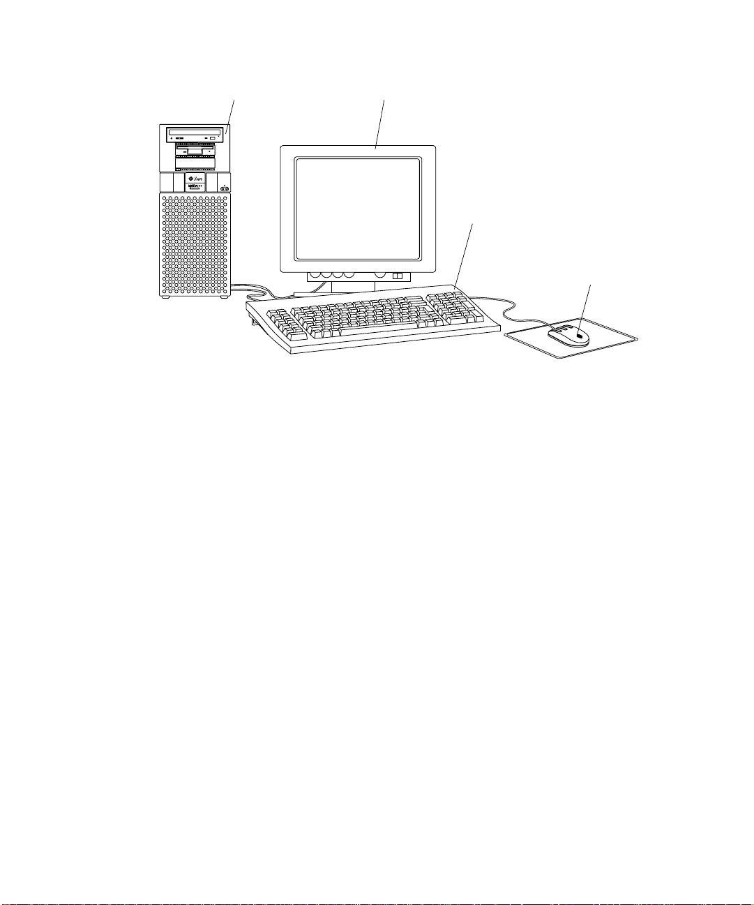
System unit
FIGURE 1-1 Ultra 60 Desktop Workstation
Monitor (24-inch optional)
Keyboard
Mouse/pad
1-2 Sun Ultra 60 Service Manual • August 2001
Page 27

1.1 I/O Devices
The Ultra 60 desktop workstation uses the I/O devices listed in TABLE1-1.
TABLE1-1 Supported I/O Devices
I/O Devices Description
20-inch (51-cm)
color monitor
24-inch (61-cm)
color monitor
Microphone
Keyboard Sun Type-5; AT 101 or UNIX layout available
Opto-mechanical
mouse
1. No longer ships with system, optional
1
1152 x 900 resolution, 76- or 66-Hz refresh rate, 84 dots per inch
(dpi)
1280 x 1024 resolution, 76- or 66-Hz refresh rate, 93 dpi
960 x 680 resolution, 112-Hz refresh rate, 70 dpi
1920 x 1200 resolution, 70-Hz refresh rate, 103 dpi
1600 x 1000 resolution, 76- or 66-Hz refresh rate, 86 dpi
1400 x 900 resolution, 76-Hz refresh rate, 77 dpi
1280 x 800 resolution, 76-Hz refresh rate, 69 dpi
SunMicrophone™II
Optomechanical, 3-button
1.2 System Unit Features
System unit components are housed in a tower configuration enclosure. Overall
enclosure dimensions (width x depth x height) are 7.50 inches (19.0 cm) x 19.60
inches (49.8 cm) x 17.70 inches (45.0 cm). System unit electronics are contained on a
single printed circuit board (motherboard). The motherboard contains the CPU
modules, memory, system control application specific integrated circuits (ASICs),
and I/O ASICs.
Chapter 1 Product Description 1-3
Page 28
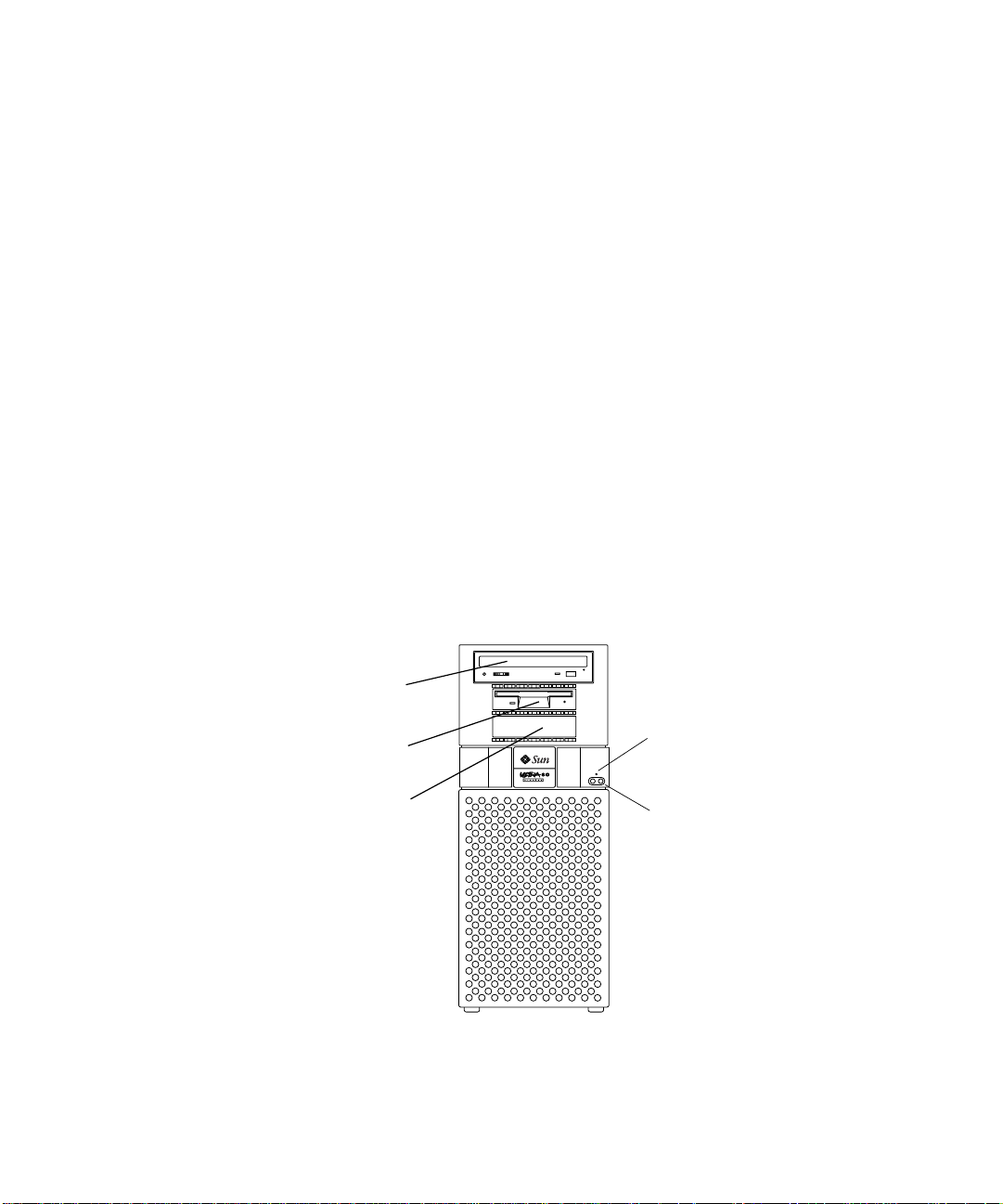
FIGURE 1-2 illustrates the system unit front view. FIGURE 1-3 illustrates the system unit
rear view. System unit electronics and peripherals contain (or may be upgraded to
contain) the following features:
■ Tower enclosure with 350-watt power supply.
■ Support for modular UltraSPARC II processor with up to a 4-megabyte (Mbyte)
Ecache and system operating frequencies from 100 megahertz (MHz) to 400 MHz.
■ 83.3-MHz to 120-MHz UPA coherent memory interconnect.
■ Use of dual in-line memory modules (DIMMs). Each group of four DIMM slots
accepts 16-, 32-, 64-, or 128-Mbyte DIMM modules. Populating with four identical
capacity DIMMs enables the memory controller for optimal system performance.
There are a total of 16 DIMM slots.
■ Four PCI slots: three 33-MHz, 64-bit or 32-bit, 5 Vdc slots; one 66-MHz or
33-MHz, 64-bit or 32-bit, 3.3 Vdc slot
■ Two UPA graphics slots.
■ 10-/100-megabits per second Ethernet.
■ 40-Mbytes per second UltraSCSI.
■ Two DB25 serial ports (synchronous and asynchronous protocols).
■ Centronics-compatible parallel port interface with extended capability port (ECP)
support.
■ Modular audio interface.
CD-ROM drive
(or tape drive)
Diskette drive
Second 3.5-inch drive bay
FIGURE 1-2 System Unit Front View
1-4 Sun Ultra 60 Service Manual • August 2001
Power LED
Power On/Standby
switch
Page 29

Parallel DB25 connector
Keyboard/mouse connector
Serial connector (2)
RS-423/RS-232
TPE connector
MII connector
68-pin SCSI connector
Audio module connector
UPA graphics (2)
PCI 66 connector 1
PCI 2, 3, 4 connector (3)
FIGURE 1-3 System Unit Rear View
AC power inlet
1.3 System Unit Components
TABLE 1-2 lists the system unit components by part number. A brief description of
each listed component is also provided.
Note – Removal and replacement of selected system unit components are also
illustrated with photographs and audio/visual instructions on the Sun Ultra 60
ShowMe How Multimedia Documentation, part number 704-5886.
Chapter 1 Product Description 1-5
Page 30

Note – Consult your authorized Sun sales representative or service provider to
confirm a part number prior to ordering a replacement part.
TABLE1-2 System Unit Replaceable Components
Component Description
Motherboard System board
Hard drive bay with SCSI Mechanical hard drive housing
4.2-Gbyte SCSI assembly Hard disk drive, 3.5-inch x 1.0-inch
9.1-Gbyte SCSI assembly Hard disk drive, 3.5-inch x 1.6-inch
PCI fan assembly PCI fan
Shroud assembly Two-CPU shroud assembly
Fan assembly CPU fan
CPU module 300-MHz, 2-Mbyte external cache
Graphics card Vertical, single buffer UPA graphics card
Graphics card Vertical, double buffer plus Z (DBZ) UPA graphics card
Power supply Power supply, 350 watts
PCI card Generic
Audio module Audio applications, 16-bit audio, 8 kHz to 48 kHz
Speaker assembly Speaker
Peripheral cable Peripheral cable
Diskette drive cable Diskette drive cable
Manual eject floppy Diskette drive, 3.5-inch, MS-DOS compatible
EMI filler panel CD-ROM drive filler panel
EMI filler panel Diskette drive filler panel
16-Mbyte DIMM 60-ns, 16-Mbyte DIMM
1-6 Sun Ultra 60 Service Manual • August 2001
Page 31

TABLE1-2 System Unit Replaceable Components (Continued)
Component Description
32-Mbyte DIMM 60-ns, 32-Mbyte DIMM
64-Mbyte DIMM 60-ns, 64-Mbyte DIMM
128-Mbyte DIMM 60-ns, 128-Mbyte DIMM
NVRAM/TOD Time of day, 48T59, with carrier
CD-ROM drive 12X-speed CD-ROM drive, 644-Mbyte SunCD™
4-mm tape drive 4-Gbyte/8-Gbyte, 4-mm tape drive, DDS-2
4-mm tape drive 12-Gbyte/24-Gbyte, 4-mm tape drive, DDS-3
8-mm tape drive 14-Gbyte, 8-mm tape drive
TPE cable (category 5) Twisted-pair Ethernet cable
DC switch assembly DC switch assembly
Chapter 1 Product Description 1-7
Page 32

1-8 Sun Ultra 60 Service Manual • August 2001
Page 33

CHAPTER
2
SunVTS Overview
This chapter contains an overview of the SunVTS™diagnostic tool.
This chapter contains the following topics:
■ SunVTS Description—page 2-1
■ SunVTS Operation—page 2-2
2.1 SunVTS Description
The SunVTS software executes multiple diagnostic hardware tests from a single user
interface. SunVTS verifies the configuration, functionality, and reliability of most
hardware controllers and devices.
The SunVTS software can be used in both the Common Desktop Environment (CDE)
and the OPEN LOOK graphical user interface (GUI) environments, or from a TTY
interface.
Within the CDE and OPEN LOOK GUI environments, test parameters can be set
quickly and easily by pointing and clicking a mouse button.
With a TTY interface, the SunVTS software is used from a terminal or modem
attached to a serial port. Data is input through the keyboard, rather than with a
mouse, and only one screen of information is displayed at a time.
2-1
Page 34

2.2 SunVTS Operation
TABLE 2-1 lists the documentation for the SunVTS software. These documents are
available on the Solaris on Sun Hardware AnswerBook, which is on the SMCC Updates
for the Solaris release.
TABLE2-1 SunVTS Documentation
Title Part Number Description
SunVTS User’s Guide 802-7299 Describes the SunVTS environment;
SunVTS Test Reference Manual 802-7300 Describes each SunVTS test; provides
SunVTS Quick Reference Card 802-7301 Provides overview of vtsui interface
starting and controlling various user
interfaces; feature descriptions
various test options and command line
arguments
features
2-2 Sun Ultra 60 Service Manual • August 2001
Page 35

CHAPTER
3
Power-On Self-Test
This chapter describes how to initiate power-on self-test (POST) diagnostics. The
examples given in this chapter are representative, details of actual test results may
be different, depending on system configurations.
This chapter contains the following topics:
■ POST Overview—page 3-2
■ Pre-POST Preparation—page 3-2
■ Initializing POST—page 3-5
■ Maximum and Minimum Levels of POST—page 3-6
■ POST Progress and Error Reporting—page 3-18
■ Bypassing POST—page 3-21
■ Additional Keyboard Control Commands—page 3-22
■ System and Keyboard LEDs—page 3-22
■ Initializing Motherboard POST—page 3-23
3-1
Page 36

3.1 POST Overview
POST is useful in determining if a portion of the system unit has failed and should
be replaced. POST detects approximately 95 percent of system unit faults and is
located in the system board OpenBoot
variables, the diag-switch? and the diag-level flag, determine if POST is
executed.
disabling POST (off), enabling POST maximum (max), or enabling POST minimum
(min).
TABLE3-1 Diag-Level Switch Settings
TABLE 3-1 lists the diag-switch? and diag-level flag settings for
™
PROM (OBP). The setting of two NVRAM
Diag-Level Setting
Off No N/A N/A N/A
Max Yes (power-on) Enabled Enabled True
Min Yes (power-on) Disabled Enabled True
POST
Initialization
Serial Port A
I/O
Serial Port A
Error Output
3.2 Pre-POST Preparation
Pre-POST preparation includes:
■ Setting up a tip connection to another workstation or terminal to view POST
progress and error messages. See Section 3.2.1, “Setting Up a Tip Connection” on
page 3-3.
■ Verifying baud rates between a workstation and a monitor or a workstation and a
terminal. See Section 3.2.2, “Verifying the Baud Rate” on page 3-4.
If a terminal or a monitor is not connected to serial port A (default port) of a
workstation or server to be tested, the keyboard LEDs are used to determine error
conditions. See Section 3.7, “System and Keyboard LEDs” on page 3-22
Diag-Switch?
Setting
3-2 Sun Ultra 60 Service Manual • August 2001
Page 37

3.2.1 Setting Up a Tip Connection
A tip connection enables a remote shell window to be used as a terminal to display
test data of a system being tested. Serial port A or serial port B of a tested system
unit is used to establish the tip connection between the system unit being tested and
another Sun workstation monitor or TTY-type terminal. The tip connection is used in
a SunOS
To set up a tip connection:
1. See
another Sun workstation using a serial null modem cable (connect cable pins 2-3,
3-2, 7-20, and 20-7).
TM
window and provides features to help with the OBP.
FIGURE 3-1. Connect serial port A of the system being tested to serial port B of
2
3
7
20
FIGURE 3-1 Setting Up a TIP Connection
2
3
7
20
2. At the other Sun workstation, check the /etc/remote file by changing to the
/etc directory and then editing the remote file:
hardwire:/ dv=/dev/term/b:br#9600:el=^C^S^Q^U^D:ie=%$:oe=^D:
Note – The example shows connection to serial port B.
3. To use serial port A:
a. Copy and paste the serial port B remote file.
b. Modify the serial port B remote file as follows:
hardwire:\ dv=/dev/term/a:br#9600:el=^C^S^Q^U^D:ie=%$:oe=^D:
Chapter 3 Power-On Self-Test 3-3
Page 38

4. In a shell window on the Sun workstation, type tip hardwire.
hostname% tip hardwire
connected
Note – The shell window is now a tip window directed to the serial port of the
system unit being tested. When power is applied to the system unit being tested,
POST messages will be displayed in this window.
5. When POST is completed, disconnect the tip window as follows:
a. Open a shell window.
b. Type ps -a to view the active tip line and process ID (PID) number.
c. Type the following to kill the tip hardwire process.
% kill -9 PID#
3.2.2 Verifying the Baud Rate
To verify the baud rate between the system unit being tested and a terminal or
another Sun workstation monitor:
1. Open a Shell window.
2. Type eeprom.
3. Verify the following serial port default settings as follows:
ttyb-mode = 9600,8,n,1
ttya-mode = 9600,8,n,1
Note – Ensure that the settings are consistent with TTY-type terminal or
workstation monitor settings.
3-4 Sun Ultra 60 Service Manual • August 2001
Page 39

3.3 Initializing POST
POST is initilized in two ways:
■ By setting the diag-switch? to true and the diag-level to max or min,
followed by power cycling the system unit
■ By simultaneously pressing the keyboard Stop and D keys while power is applied
to the system unit
To set the diag-switch? to true and power cycle the system unit:
1. At the system prompt, type:
ok setenv diag-switch? true
2. At the keyboard, power cycle the system unit by simultaneously pressing the
Shift key and the power-on key (
power-on key again.
FIGURE 3-2). After a few seconds, press the
Stop key D key
Caps Lock
key indicator
FIGURE 3-2 Sun Type-5 Keyboard
Shift key Compose
indicator
Scroll Lock
key indicator
key indicator
Power-on key
Num Lock
key indicator
Chapter 3 Power-On Self-Test 3-5
Page 40

3. Verify the following:
a. The display prompt is no longer displayed.
b. The monitor power-on indicator flashes on and off.
c. The keyboard Caps Lock key indicator flashes on and off.
4. When the POST is complete, type the following at the system prompt:
ok setenv diag-switch? false
3.4 Maximum and Minimum Levels of POST
Two levels of POST are available: maximum (max) level and minimum (min) level.
The system initiates the selected level of POST based upon the setting of
diag-level, a NVRAM variable.
The default setting for diag-level is max. An example of a max level POST output
on serial port A is provided in Section 3.4.1, “diag-level Variable Set to max” on
page 3-7 An example of a min level POST output on serial port A is provided in
Section 3.4.2, “diag-level Variable Set to min” on page 3-14.
To set the diag-level variable to min, type:
ok setenv diag-level min
To return to the default setting
ok setenv diag-level max
3-6 Sun Ultra 60 Service Manual • August 2001
:
Page 41

3.4.1 diag-level Variable Set to max
When the diag-level variable is set to max, POST enables an extended set of
diagnostic-level tests. This mode requires approximately 2 minutes and 15 seconds
to complete (with 128 Mbytes of DIMM installed).
typical serial port A POST output with the diag-level variable set to max
CODE EXAMPLE 3-1 diag-level Variable Set to max
Executing Power On SelfTest
0>
0>@(#) Sun Ultra 60(UltraSPARC-II 2-way) UPA/PCI POST x.x.x
xx/xx/xxxx xx:xx PM
0>INFO: Processor 0 is master.
0>
0> <00> Init System BSS
0> <00> NVRAM Battery Detect Test
0> <00> NVRAM Scratch Addr Test
0> <00> DMMU TLB Tag Access Test
0> <00> DMMU TLB RAM Access Test
0> <00> IMMU TLB Tag Access Test
0> <00> IMMU TLB RAM Access Test
0> <00> Probe Ecache
0>INFO:CPU 296 MHz: 2048KB Ecache
0> <00> Ecache RAM Addr Test
0> <00> Ecache Tag Addr Test
0> <00> Ecache Tag Test
0> <00> Invalidate Ecache Tags
0>INFO: Processor 2 - UltraSPARC-II.
0> <00> Init SC Regs
0> <00> SC Address Reg Test
0> <00> SC Reg Index Test
0> <00> SC Regs Test
0> <00> SC Dtag RAM Addr Test
0> <00> SC Cache Size Init
0> <00> SC Dtag RAM Data Test
0> <00> SC Dtag Init
0> <00> Probe Memory
0>INFO:128MB Bank 0
0>INFO: 0MB Bank 1
0>INFO: 0MB Bank 2
0>INFO: 0MB Bank 3
0> <00> Malloc Post Memory
0> <00> Init Post Memory
0> <00> Post Memory Addr Test
0> <00> Map PROM/STACK/NVRAM in DMMU
0> <00>Memory Stack Test
CODE EXAMPLE 3-1 identifies a
Chapter 3 Power-On Self-Test 3-7
Page 42

CODE EXAMPLE 3-1 diag-level Variable Set to max (Continued)
2> <00> DMMU TLB Tag Access Test
2> <00> DMMU TLB RAM Access Test
2> <00> IMMU TLB Tag Access Test
2> <00> IMMU TLB RAM Access Test
2> <00> Probe Ecache
2>INFO:CPU 296 MHz: 2048KB Ecache
2> <00> Ecache RAM Addr Test
2> <00> Ecache Tag Addr Test
2> <00> Ecache Tag Test
2> <00> Invalidate Ecache Tags
2> <00> Map PROM/STACK/NVRAM in DMMU
2> <00> Update Slave Stack/Frame Ptrs
0> <00> DMMU Hit/Miss Test
0> <00> IMMU Hit/Miss Test
0> <00> DMMU Little Endian Test
0> <00> IU ASI Access Test
0> <00> FPU ASI Access Test
2> <00> DMMU Hit/Miss Test
2> <00> IMMU Hit/Miss Test
2> <00> DMMU Little Endian Test
2> <00> IU ASI Access Test
2> <00> FPU ASI Access Test
2> <00> Dcache RAM Test
2> <00> Dcache Tag Test
2> <00> Icache RAM Test
2> <00> Icache Tag Test
2> <00> Icache Next Test
2> <00> Icache Predecode Test
0> <1f> Init Psycho
0> <1f> PIO Read Error, Master Abort Test
0> <1f> PIO Read Error, Target Abort Test
0> <1f> PIO Write Error, Master Abort Test
0> <1f> PIO Write Error, Target Abort Test
0> <1f> Timer Increment Test
0> <1f> Consistent DMA UE ECC Rd Err Lpbk Test
0> <1f> Pass-Thru DMA UE ECC Rd Err Lpbk Test
0> <00> Copy Post to Memory
0> <00> Ecache Thrash Test
0> <00> Init Memory
0> <00> Memory Addr w/ Ecache Test
0>INFO:128MB Bank 0
0>INFO: 0MB Bank 1
0>INFO: 0MB Bank 2
0>INFO: 0MB Bank 3
0> <00> Block Memory Addr Test
0>INFO:128MB Bank 0
0>INFO: 0MB Bank 1
3-8 Sun Ultra 60 Service Manual • August 2001
Page 43

CODE EXAMPLE 3-1 diag-level Variable Set to max (Continued)
0>INFO: 0MB Bank 2
0>INFO: 0MB Bank 3
0> <00> ECC Memory Addr Test
0>INFO:128MB Bank 0
0>INFO: 0MB Bank 1
0>INFO: 0MB Bank 2
0>INFO: 0MB Bank 3
0> <00> Memory Status Test
0>INFO:128MB Bank 0
0>INFO: 0MB Bank 1
0>INFO: 0MB Bank 2
0>INFO: 0MB Bank 3
0> <00> V9 Instruction Test
0> <00> CPU Tick and Tick Compare Reg Test
0> <00> CPU Soft Trap Test
0> <00> CPU Softint Reg and Int Test
2> <00> V9 Instruction Test
2> <00> CPU Tick and Tick Compare Reg Test
0> <1f> Init Psycho
0> <1f> Psycho Cntl and UPA Reg Test
0> <1f> Psycho DMA Scoreboard Reg Test
0> <1f> Psycho Perf Cntl Reg Test
0> <1f> PIO Decoder and BCT Test
0> <1f> PCI Byte Enable Test
0> <1f> Counter/Timer Limit Regs Test
0> <1f> Timer Reload Test
0> <1f> Timer Periodic Test
0> <1f> Mondo Int Map (short) Reg Test
0> <1f> Mondo Int Set/Clr Reg Test
0> <1f> Psycho IOMMU Regs Test
0> <1f> Psycho IOMMU RAM Address Test
0> <1f> Psycho IOMMU CAM Address Test
0> <1f> IOMMU TLB Compare Test
0> <1f> IOMMU TLB Flush Test
0> <1f> Stream Buff A Control Reg Test
0> <1f> Psycho ScacheA Page Tag Addr Test
0> <1f> Psycho ScacheA Line Tag Addr Test
0> <1f> Psycho ScacheA RAM Addr Test
0> <1f> Psycho ScacheA Error Status NTA Test
0> <1f> Psycho ScacheB Page Tag Addr Test
0> <1f> Psycho ScacheB Line Tag Addr Test
0> <1f> Psycho ScacheB RAM Addr Test
0> <1f> Psycho ScacheB Error Status NTA Test
0> <1f> PBMA PCI Config Space Regs Test
0> <1f> PBMA Control/Status Reg Test
0> <1f> PBMA Diag Reg Test
0> <1f> PBMB PCI Config Space Regs Test
Chapter 3 Power-On Self-Test 3-9
Page 44

CODE EXAMPLE 3-1 diag-level Variable Set to max (Continued)
0> <1f> PBMB Control/Status Reg Test
0> <1f> PBMB Diag Reg Test
0> <00> FPU Regs Test
0> <00> FPU Move Regs Test
0> <00> FPU State Reg Test
0> <00> FPU Functional Test
0> <00> FPU Trap Test
0> <00> DMMU Primary Context Reg Test
0> <00> DMMU Secondary Context Reg Test
0> <00> DMMU TSB Reg Test
0> <00> DMMU Tag Access Reg Test
0> <00> DMMU VA Watchpoint Reg Test
0> <00> DMMU PA Watchpoint Reg Test
0> <00> IMMU TSB Reg Test
0> <00> IMMU Tag Access Reg Test
0> <00> DMMU TLB Tag Access Test
0> <00> DMMU TLB RAM Access Test
0> <00> Dcache RAM Test
0> <00> Dcache Tag Test
0> <00> Icache RAM Test
0> <00> Icache Tag Test
0> <00> Icache Next Test
0> <00> Icache Predecode Test
2> <00> FPU Regs Test
2> <00> FPU Move Regs Test
2> <00> FPU State Reg Test
2> <00> FPU Functional Test
2> <00> FPU Trap Test
2> <00> DMMU Primary Context Reg Test
2> <00> DMMU Secondary Context Reg Test
2> <00> DMMU TSB Reg Test
2> <00> DMMU Tag Access Reg Test
2> <00> DMMU VA Watchpoint Reg Test
2> <00> DMMU PA Watchpoint Reg Test
2> <00> IMMU TSB Reg Test
2> <00> IMMU Tag Access Reg Test
2> <00> DMMU TLB Tag Access Test
2> <00> DMMU TLB RAM Access Test
0> <00> CPU Addr Align Trap Test
0> <00> DMMU Access Priv Page Test
0> <00> DMMU Write Protected Page Test
0> <1f> Init Psycho
0> <1f> Pri CE ECC Error Test
0> <1f> Pri UE ECC Error Test
0> <1f> Pri 2 bit w/ bit hole UE ECC Err Test
0> <1f> Pri 3 bit UE ECC Err Test
0> <1f> Streaming DMA UE ECC Rd Err Ebus Test
3-10 Sun Ultra 60 Service Manual • August 2001
Page 45

CODE EXAMPLE 3-1 diag-level Variable Set to max (Continued)
0> <1f> Streaming DMA CE ECC Rd Err Ebus Test
0> <1f> Streaming DMA CE ECC Rd Err Lpbk Test
0> <1f> Consistent DMA UE ECC Rd Error Ebus Test
0> <1f> Consistent DMA UE ECC R/M/W Err Ebus Test
0> <1f> Consistent DMA UE ECC R/M/W Err Lpbk Test
0> <1f> Consistent DMA CE ECC Rd Err Ebus Test
0> <1f> Consistent DMA CE ECC Rd Err Lpbk Test
0> <1f> Consistent DMA CE ECC R/M/W Err Ebus Test
0> <1f> Consistent DMA CE ECC R/M/W Err Lpbk Test
0> <1f> Consistent DMA Wr Data Parity Err Lpbk Test
0> <1f> Pass-Thru DMA UE ECC Rd Err Ebus Test
0> <1f> Pass-Thru DMA UE ECC R/M/W Err Ebus Test
0> <1f> Pass-Thru DMA UE ECC R/M/W Err Lpbk Test
0> <1f> Pass-Thru DMA CE ECC Rd Err Ebus Test
0> <1f> Pass-Thru DMA CE ECC Rd Err Lpbk Test
0> <1f> Pass-Thru DMA CE ECC R/M/W Err Ebus Test
0> <1f> Pass-Thru DMA CE ECC R/M/W Err Lpbk Test
0> <1f> Pass-Thru DMA Write Data Parity Err, Lpbk Test
0> <1f> Init Psycho
0> <1f> Mondo Generate Interrupt Test
0> <1f> Timer Interrupt Test
0> <1f> Timer Interrupt w/ periodic Test
0> <1f> Psycho Stream Buff A Flush Sync Test
0> <1f> Psycho Stream Buff B Flush Sync Test
0> <1f> Psycho Stream Buff A Flush Invalidate Test
0> <1f> Psycho Stream Buff B Flush Invalidate Test
0> <1f> Psycho Merge Buffer w/ Scache A Test
0> <1f> Psycho Merge Buffer w/ Scache B Test
0> <1f> Consist DMA Rd, IOMMU miss Ebus Test
0> <1f> Consist DMA Rd, IOMMU miss Lpbk Test
0> <1f> Consist DMA Rd, IOMMU hit Ebus Test
0> <1f> Consist DMA Rd, IOMMU hit Lpbk Test
0> <1f> Consist DMA Wr, IOMMU miss Ebus Test
0> <1f> Consist DMA Wr, IOMMU miss Lpbk Test
0> <1f> Consist DMA Wr, IOMMU hit Ebus Test
0> <1f> Consist DMA Wr, IOMMU hit Lpbk Test
0> <1f> Stream DMA Rd, IOMMU miss, Scache Miss Ebus Test
0> <1f> Stream DMA Rd, IOMMU miss, Scache Miss Lpbk Test
0> <1f> Stream DMA Rd, IOMMU hit, Scache Miss Ebus Test
0> <1f> Stream DMA Rd, IOMMU hit, Scache Miss Lpbk Test
0> <1f> Stream DMA Rd, IOMMU Miss, Scache(prev rd) Hit Ebus Test
0> <1f> Stream DMA Rd, IOMMU Miss, Scache Hit (prev rd) Lpbk Test
0> <1f> Stream DMA Rd, IOMMU Hit, Scache Hit Ebus Test
0> <1f> Stream DMA Rd, IOMMU Hit, Scache Hit (prev rd) Lpbk Test
0> <1f> Stream DMA Rd, IOMMU Miss, Scache Hit(prev wr) Ebus Test
0> <1f> Stream DMA Rd, IOMMU Miss, Scache Hit (prev wr) Lpbk Test
0> <1f> Stream DMA Rd, IOMMU Hit, Scache Hit(prev wr) Ebus Test
Chapter 3 Power-On Self-Test 3-11
Page 46

CODE EXAMPLE 3-1 diag-level Variable Set to max (Continued)
0> <1f> Stream DMA Rd, IOMMU Hit, Scache Hit (prev wr) Lpbk Test
0> <1f> Stream DMA Wr, IOMMU miss, Scache Miss Ebus Test
0> <1f> Stream DMA Wr, IOMMU miss, Scache Miss Lpbk Test
0> <1f> Stream DMA Wr, IOMMU hit, Scache Miss Ebus Test
0> <1f> Stream DMA Wr, IOMMU hit, Scache Miss Lpbk Test
0> <1f> Stream DMA Wr, IOMMU Miss, Scache(prev rd) Hit Ebus Test
0> <1f> Stream DMA Wr, IOMMU Miss, Scache(prev rd) Hit Lpbk Test
0> <1f> Stream DMA Wr, IOMMU Hit, Scache(prev rd) Hit Ebus Test
0> <1f> Stream DMA Wr, IOMMU Hit, Scache(prev rd) Hit Lpbk Test
0> <1f> Stream DMA Wr, IOMMU Miss, Scache(prev wr) Hit Ebus Test
0> <1f> Stream DMA Wr, IOMMU Miss, Scache(prev wr) Hit Lpbk Test
0> <1f> Stream DMA Wr, IOMMU Hit, Scache(prev wr) Hit Ebus Test
0> <1f> Stream DMA Wr, IOMMU Hit, Scache(prev wr) Hit Lpbk Test
0> <1f> Pass-Thru DMA Rd, Ebus device Test
0> <1f> Pass-Thru DMA Rd, Loopback Mode Test
0> <1f> Pass-Thru DMA Wr, Ebus device Test
0> <1f> Pass-Thru DMA Wr, Loopback Mode Test
0> <1f> Consist DMA Rd, IOMMU LRU Lock Ebus Test
0> <1f> Consist DMA Rd, IOMMU LRU Lock Lpbk Test
0> <1f> Stream DMA Rd, IOMMU LRU Lock, Scache LRU Lock Ebus Test
0> <1f> Stream DMA Rd, IOMMU LRU Lock, Scache LRU Lock Lpbk Test
0> <1f> Stream DMA Rd, IOMMU miss, Scache LRU Lock Ebus Test
0> <1f> Stream DMA Rd, IOMMU Miss, Scache LRU Lock Lpbk Test
0> <1f> Stream DMA Rd, IOMMU Hit, Scache LRU Lock Ebus Test
0> <1f> Stream DMA Rd, IOMMU Hit, Scache LRU Lock Lpbk Test
0> <1f> Stream DMA Rd, IOMMU LRU Lock, Scache Miss Ebus Test
0> <1f> Stream DMA Rd, IOMMU LRU Lock, Scache Miss Lpbk Test
0> <1f> Consist DMA Wr, IOMMU LRU Locked Ebus Test
0> <1f> Consist DMA Wr, IOMMU LRU Lock Lpbk Test
0> <1f> Stream DMA Wr, IOMMU LRU Lock, Scache LRU Lock Ebus Test
0> <1f> Stream DMA Wr, IOMMU LRU Lock, Scache LRU Lock Lpbk Test
0> <1f> Stream DMA Wr, IOMMU Miss, Scache LRU Lock Ebus Test
0> <1f> Stream DMA Wr, IOMMU Miss, Scache LRU Lock Lpbk Test
0> <1f> Stream DMA Wr, IOMMU Hit, Scache LRU Lock Ebus Test
0> <1f> Stream DMA Wr, IOMMU Hit, Scache LRU Lock Lpbk Test
0> <1f> Stream DMA Wr, IOMMU LRU Lock, Scache Miss Ebus Test
0> <1f> Stream DMA Wr, IOMMU LRU Lock, Scache Miss Lpbk Test
0> <1f> Stream DMA Wr, IOMMU LRU Lock, Scache(prev rd) Hit Ebus
Test
0> <1f> Stream DMA Wr, IOMMU LRU Lock, Scache(prev rd) Hit Lpbk
Test
0> <00> Init Memory
0>INFO:128MB Bank 0
0>INFO: 0MB Bank 1
0>INFO: 0MB Bank 2
0>INFO: 0MB Bank 3
0> <00> Memory w/ Ecache Test
3-12 Sun Ultra 60 Service Manual • August 2001
Page 47

CODE EXAMPLE 3-1 diag-level Variable Set to max (Continued)
0>INFO:128MB Bank 0
0>INFO: 0MB Bank 1
0>INFO: 0MB Bank 2
0>INFO: 0MB Bank 3
0> <00> Block Memory Test
0>INFO:128MB Bank 0
0>INFO: 0MB Bank 1
0>INFO: 0MB Bank 2
0>INFO: 0MB Bank 3
0> <00> ECC Blk Memory Test
0>INFO:128MB Bank 0
0>INFO: 0MB Bank 1
0>INFO: 0MB Bank 2
0>INFO: 0MB Bank 3
0> <00> UltraSPARC-2 Prefetch Instructions Test
0> <00>Test 0: prefetch_mr
0> <00>Test 1: prefetch to non-cacheable page
0> <00>Test 2: prefetch to page with dmmu misss
0> <00>Test 3: prefetch miss does not check alignment
0> <00>Test 4: prefetcha with asi 0x4c is noped
0> <00>Test 5: prefetcha with asi 0x54 is noped
0> <00>Test 6: prefetcha with asi 0x6e is noped
0> <00>Test 7: prefetcha with asi 0x76 is noped
0> <00>Test 8: prefetch with fcn 5
0> <00>Test 9: prefetch with fcn 2
0> <00>Test 10: prefetch with fcn 12
0> <00>Test 11: prefetch with fcn 16 is noped
0> <00>Test 12: prefetch with fcn 29 is noped
0> <00>Test 13: prefetcha with asi 0x15 is noped
0> <00>Test 14: prefetch with fcn 3
0> <00>Test 15: prefetcha14 with fcn 2
0> <00>Test 16: prefetcha80_mr
0> <00>Test 17: prefetcha81_1r
0> <00>Test 18: prefetcha10_mw
0> <00>Test 19: prefetcha80_17 is noped
0> <00>Test 20: prefetcha10_6: illegal instruction trap
0> <00>Test 21: prefetcha11_1w
0> <00>Test 22: prefetcha81_31
0> <00>Test 23: prefetcha11_15: illegal instruction trap
2> <00> UltraSPARC-2 Prefetch Instructions Test
2> <00>Test 0: prefetch_mr
2> <00>Test 1: prefetch to non-cacheable page
2> <00>Test 2: prefetch to page with dmmu misss
2> <00>Test 3: prefetch miss does not check alignment
2> <00>Test 4: prefetcha with asi 0x4c is noped
2> <00>Test 5: prefetcha with asi 0x54 is noped
2> <00>Test 6: prefetcha with asi 0x6e is noped
Chapter 3 Power-On Self-Test 3-13
Page 48

CODE EXAMPLE 3-1 diag-level Variable Set to max (Continued)
2> <00>Test 7: prefetcha with asi 0x76 is noped
2> <00>Test 8: prefetch with fcn 5
2> <00>Test 9: prefetch with fcn 2
2> <00>Test 10: prefetch with fcn 12
2> <00>Test 11: prefetch with fcn 16 is noped
2> <00>Test 12: prefetch with fcn 29 is noped
2> <00>Test 13: prefetcha with asi 0x15 is noped
2> <00>Test 14: prefetch with fcn 3
2> <00>Test 15: prefetcha14 with fcn 2
2> <00>Test 16: prefetcha80_mr
2> <00>Test 17: prefetcha81_1r
2> <00>Test 18: prefetcha10_mw
2> <00>Test 19: prefetcha80_17 is noped
2> <00>Test 20: prefetcha10_6: illegal instruction trap
2> <00>Test 21: prefetcha11_1w
2> <00>Test 22: prefetcha81_31
2> <00>Test 23: prefetcha11_15: illegal instruction trap
0>STATUS =PASSED
Power On Selftest Completed
3.4.2 diag-level Variable Set to min
When the diag-level variable is set to min, POST enables an abbreviated set of
diagnostic-level tests. This mode requires approximately 1 minute and 30 seconds to
complete (with 128 Mbytes of DIMM installed).
port A POST output with the diag-level NVRAM variable set to min.
CODE EXAMPLE 3-2 diag-level Variable Set to min
Executing Power On SelfTest
0>
0>@(#) Sun Ultra 60(UltraSPARC-II 2-way) UPA/PCI POST x.x.x
xx/xx/xxxx xx:xx PM
0>INFO: Processor 0 is master.
0>
0> <00> Init System BSS
0> <00> NVRAM Battery Detect Test
0> <00> NVRAM Scratch Addr Test
0> <00> DMMU TLB Tag Access Test
0> <00> DMMU TLB RAM Access Test
0> <00> IMMU TLB Tag Access Test
3-14 Sun Ultra 60 Service Manual • August 2001
CODE EXAMPLE 3-2 identifies a serial
Page 49

CODE EXAMPLE 3-2 diag-level Variable Set to min (Continued)
0> <00> IMMU TLB RAM Access Test
0> <00> Probe Ecache
0>INFO:CPU 296 MHz: 2048KB Ecache
0> <00> Ecache RAM Addr Test
0> <00> Ecache Tag Addr Test
0> <00> Ecache Tag Test
0> <00> Invalidate Ecache Tags
0>INFO: Processor 2 - UltraSPARC-II.
0> <00> Init SC Regs
0> <00> SC Address Reg Test
0> <00> SC Reg Index Test
0> <00> SC Regs Test
0> <00> SC Dtag RAM Addr Test
0> <00> SC Cache Size Init
0> <00> SC Dtag RAM Data Test
0> <00> SC Dtag Init
0> <00> Probe Memory
0>INFO:128MB Bank 0
0>INFO: 0MB Bank 1
0>INFO: 0MB Bank 2
0>INFO: 0MB Bank 3
0> <00> Malloc Post Memory
0> <00> Init Post Memory
0> <00> Post Memory Addr Test
0> <00> Map PROM/STACK/NVRAM in DMMU
0> <00>Memory Stack Test
2> <00> DMMU TLB Tag Access Test
2> <00> DMMU TLB RAM Access Test
2> <00> IMMU TLB Tag Access Test
2> <00> IMMU TLB RAM Access Test
2> <00> Probe Ecache
2>INFO:CPU 296 MHz: 2048KB Ecache
2> <00> Ecache RAM Addr Test
2> <00> Ecache Tag Addr Test
2> <00> Ecache Tag Test
2> <00> Invalidate Ecache Tags
2> <00> Map PROM/STACK/NVRAM in DMMU
2> <00> Update Slave Stack/Frame Ptrs
0> <00> DMMU Hit/Miss Test
0> <00> IMMU Hit/Miss Test
0> <00> DMMU Little Endian Test
0> <00> IU ASI Access Test
0> <00> FPU ASI Access Test
2> <00> DMMU Hit/Miss Test
2> <00> IMMU Hit/Miss Test
2> <00> DMMU Little Endian Test
2> <00> IU ASI Access Test
Chapter 3 Power-On Self-Test 3-15
Page 50

CODE EXAMPLE 3-2 diag-level Variable Set to min (Continued)
2> <00> FPU ASI Access Test
2> <00> Dcache RAM Test
2> <00> Dcache Tag Test
2> <00> Icache RAM Test
2> <00> Icache Tag Test
2> <00> Icache Next Test
2> <00> Icache Predecode Test
0> <1f> Init Psycho
0> <1f> PIO Read Error, Master Abort Test
0> <1f> PIO Read Error, Target Abort Test
0> <1f> PIO Write Error, Master Abort Test
0> <1f> PIO Write Error, Target Abort Test
0> <1f> Timer Increment Test
0> <1f> Consistent DMA UE ECC Rd Err Lpbk Test
0> <1f> Pass-Thru DMA UE ECC Rd Err Lpbk Test
0> <00> Copy Post to Memory
0> <00> Ecache Thrash Test
0> <00> Init Memory
0> <00> Memory Addr w/ Ecache Test
0>INFO:128MB Bank 0
0>INFO: 0MB Bank 1
0>INFO: 0MB Bank 2
0>INFO: 0MB Bank 3
0> <00> Block Memory Addr Test
0>INFO:128MB Bank 0
0>INFO: 0MB Bank 1
0>INFO: 0MB Bank 2
0>INFO: 0MB Bank 3
0> <00> ECC Memory Addr Test
0>INFO:128MB Bank 0
0>INFO: 0MB Bank 1
0>INFO: 0MB Bank 2
0>INFO: 0MB Bank 3
0> <00> Memory Status Test
0>INFO:128MB Bank 0
0>INFO: 0MB Bank 1
0>INFO: 0MB Bank 2
0>INFO: 0MB Bank 3
0> <00> V9 Instruction Test
0> <00> CPU Tick and Tick Compare Reg Test
0> <00> CPU Soft Trap Test
0> <00> CPU Softint Reg and Int Test
2> <00> V9 Instruction Test
2> <00> CPU Tick and Tick Compare Reg Test
0> <1f> Init Psycho
0> <1f> Psycho Cntl and UPA Reg Test
0> <1f> Psycho DMA Scoreboard Reg Test
3-16 Sun Ultra 60 Service Manual • August 2001
Page 51

CODE EXAMPLE 3-2 diag-level Variable Set to min (Continued)
0> <1f> Psycho Perf Cntl Reg Test
0> <1f> PIO Decoder and BCT Test
0> <1f> PCI Byte Enable Test
0> <1f> Counter/Timer Limit Regs Test
0> <1f> Timer Reload Test
0> <1f> Timer Periodic Test
0> <1f> Mondo Int Map (short) Reg Test
0> <1f> Mondo Int Set/Clr Reg Test
0> <1f> Psycho IOMMU Regs Test
0> <1f> Psycho IOMMU RAM Address Test
0> <1f> Psycho IOMMU CAM Address Test
0> <1f> IOMMU TLB Compare Test
0> <1f> IOMMU TLB Flush Test
0> <1f> Stream Buff A Control Reg Test
0> <1f> Psycho ScacheA Page Tag Addr Test
0> <1f> Psycho ScacheA Line Tag Addr Test
0> <1f> Psycho ScacheA RAM Addr Test
0> <1f> Psycho ScacheA Error Status NTA Test
0> <1f> Psycho ScacheB Page Tag Addr Test
0> <1f> Psycho ScacheB Line Tag Addr Test
0> <1f> Psycho ScacheB RAM Addr Test
0> <1f> Psycho ScacheB Error Status NTA Test
0> <1f> PBMA PCI Config Space Regs Test
0> <1f> PBMA Control/Status Reg Test
0> <1f> PBMA Diag Reg Test
0> <1f> PBMB PCI Config Space Regs Test
0> <1f> PBMB Control/Status Reg Test
0> <1f> PBMB Diag Reg Test
0> <00> UltraSPARC-2 Prefetch Instructions Test
0> <00>Test 0: prefetch_mr
0> <00>Test 1: prefetch to non-cacheable page
0> <00>Test 2: prefetch to page with dmmu misss
0> <00>Test 3: prefetch miss does not check alignment
0> <00>Test 4: prefetcha with asi 0x4c is noped
0> <00>Test 5: prefetcha with asi 0x54 is noped
0> <00>Test 6: prefetcha with asi 0x6e is noped
0> <00>Test 7: prefetcha with asi 0x76 is noped
0> <00>Test 8: prefetch with fcn 5
0> <00>Test 9: prefetch with fcn 2
0> <00>Test 10: prefetch with fcn 12
0> <00>Test 11: prefetch with fcn 16 is noped
0> <00>Test 12: prefetch with fcn 29 is noped
0> <00>Test 13: prefetcha with asi 0x15 is noped
0> <00>Test 14: prefetch with fcn 3
0> <00>Test 15: prefetcha14 with fcn 2
0> <00>Test 16: prefetcha80_mr
0> <00>Test 17: prefetcha81_1r
Chapter 3 Power-On Self-Test 3-17
Page 52

CODE EXAMPLE 3-2 diag-level Variable Set to min (Continued)
0> <00>Test 18: prefetcha10_mw
0> <00>Test 19: prefetcha80_17 is noped
0> <00>Test 20: prefetcha10_6: illegal instruction trap
0> <00>Test 21: prefetcha11_1w
0> <00>Test 22: prefetcha81_31
0> <00>Test 23: prefetcha11_15: illegal instruction trap
2> <00> UltraSPARC-2 Prefetch Instructions Test
2> <00>Test 0: prefetch_mr
2> <00>Test 1: prefetch to non-cacheable page
2> <00>Test 2: prefetch to page with dmmu misss
2> <00>Test 3: prefetch miss does not check alignment
2> <00>Test 4: prefetcha with asi 0x4c is noped
2> <00>Test 5: prefetcha with asi 0x54 is noped
2> <00>Test 6: prefetcha with asi 0x6e is noped
2> <00>Test 7: prefetcha with asi 0x76 is noped
2> <00>Test 8: prefetch with fcn 5
2> <00>Test 9: prefetch with fcn 2
2> <00>Test 10: prefetch with fcn 12
2> <00>Test 11: prefetch with fcn 16 is noped
2> <00>Test 12: prefetch with fcn 29 is noped
2> <00>Test 13: prefetcha with asi 0x15 is noped
2> <00>Test 14: prefetch with fcn 3
2> <00>Test 15: prefetcha14 with fcn 2
2> <00>Test 16: prefetcha80_mr
2> <00>Test 17: prefetcha81_1r
2> <00>Test 18: prefetcha10_mw
2> <00>Test 19: prefetcha80_17 is noped
2> <00>Test 20: prefetcha10_6: illegal instruction trap
2> <00>Test 21: prefetcha11_1w
2> <00>Test 22: prefetcha81_31
2> <00>Test 23: prefetcha11_15: illegal instruction trap
0>STATUS =PASSED
Power On Selftest Completed
3.4.3 POST Progress and Error Reporting
While POST is initialized, the Caps Lock key on the Sun Type-5 keyboard flashes on
and off to indicate that POST tests are being executed. Additional POST progress
indications are also visible when a TTY-type terminal or a tip line is connected
between serial port A (default port) of the system being tested and a POST
monitoring system.
3-18 Sun Ultra 60 Service Manual • August 2001
Page 53

If an error occurs during the POST execution, the keyboard Caps Lock key indicator
stops flashing and an error code is displayed using the Caps Lock, Compose, Scroll
Lock, and Num Lock key indicators. The error code indicates a particular system
hardware failure.
Note – An error code may only be visible for a few seconds. Observe the Caps Lock,
Compose, Scroll Lock, and Num Lock key indicators closely while POST is active.
In most cases, POST also attempts to send a failure message to the POST monitoring
system.
CODE EXAMPLE 3-3 identifies the typical appearance of a failure message. If a
keyboard error code is displayed, determine the meaning of the error code by
comparing the keyboard error code pattern to the corresponding error code meaning
listed in
TABLE 3-2.
Note – The system unit does not automatically boot if a POST error occurs; it halts
at the ok prompt to alert the user of a failure.
CODE EXAMPLE 3-3 Typical Error Code Failure Message
Executing Power On SelfTest
0>
0>@(#) Sun UltraSPARC-II 2-way(Deuterium) UPA/PCI POST 1.0.3
08/15/97: 11:36
0>INFO: Processor 0 is master.
0>
0> <00> Init System BSS
0> <00> NVRAM Battery Detect Test
0> <00> NVRAM Scratch Addr Test
0> <00> DMMU TLB Tag Access Test
0> <00> DMMU TLB RAM Access Test
0> <00> Probe Ecache
0>INFO:CPU 296 MHz: 2048KB Ecache
0> <00> Ecache RAM Addr Test
0> <00> Ecache Tag Addr Test
0> <00> Invalidate Ecache Tags
0>INFO: Min Psycho configuration.
0>INFO: Processor 2 - UltraSPARC-II.
0> <00> Init SC Regs
0> <00> SC Address Reg Test
0> <00> SC Reg Index Test
0> <00> SC Regs Test
0> <00> SC Dtag RAM Addr Test
0> <00> SC Cache Size Init
Chapter 3 Power-On Self-Test 3-19
Page 54

CODE EXAMPLE 3-3 Typical Error Code Failure Message (Continued)
0> <00> SC Dtag Init
0> <00> Probe Memory
0>INFO:128MB Bank 0
0>INFO:No memory detected in Bank 1
0>INFO:No memory detected in Bank 2
0>INFO:No memory detected in Bank 3
0> <00> Malloc Post Memory
0> <00> Init Post Memory
0> <00> Post Memory Addr Test
0>mem_utils.c mem_err_bd_desc = 00000000.00000000, xor =
80808000.80808080
0>STATUS =FAILED
0>TEST =Post Memory Addr
TTF =0
PASSES =1
ERRORS =1
SUSPECT=SIMM U0801
0>MESSAGE=Mem Addr line compare error
addr 00000000.00000000
exp 00000000.00000000
obs 80808000.80808080
0> xor 80808000.80808080
0> Verbose Data Path Information:
0> Addr = 00000000.00000000
0> PATH SUSPECT= SDB U0301
0> PATH SUSPECT= XBAR U301
0> <00>Memory Stack Test
0>STATUS =FAILED
0>TEST =Post Memory Addr
TTF =0
PASSES =1
ERRORS =1
SUSPECT=SIMM U0801
0>MESSAGE=Memory compare error
addr 00000000.007f8080
exp 55555555.557fd5d5
obs 15151515.15151505
3-20 Sun Ultra 60 Service Manual • August 2001
Page 55

TABLE3-2 Keyboard LED Patterns
Caps Lock Compose Scroll Lock Num Lock Meaning of Pattern
On Off Off Off System motherboard
Off On Off Off CPU module 0
Off On On Off CPU module 1
On Off Off On No memory detected
On On Off Off Memory bank 0
On On Off On Memory bank 1
On On On Off Memory bank 2
On On On On Memory bank 3
Off Off Off On NVRAM
3.5 Bypassing POST
POST can be disabled and thereby bypassed. To bypass POST:
1. Prior to powering on the system, press and hold the Stop key on the keyboard
(
FIGURE 3-2).
2. With the Stop key pressed, turn on the system by pressing the power-on key.
Chapter 3 Power-On Self-Test 3-21
Page 56

3.6 Additional Keyboard Control Commands
■ Stop Key
If the diag-level is set to either max or min and the diag-level switch? variable
is set to true and POST is not to be executed when the system is powered on, press
and hold the keyboard Stop key and press the keyboard power-on key.
Note – Press and hold the Stop key for approximately 5 seconds.
■ Stop and N Keys
To set the system NVRAM parameters to the original default settings, press and hold
the Stop and N keys before powering on the system. Continue to hold the Stop and
N keys until the system banner displays on the monitor.
3.7 System and Keyboard LEDs
The power light-emitting diode (LED), located at the chassis front, remains lighted
when the system is operating normally.
LED.
FIGURE 1-2 shows the location of the power
While POST is executing and making progress, the Caps Lock key LED blinks while
the rest of the LEDs are off. If POST finds an error, a pattern is encoded in the LEDs
to indicate the defective part. If POST completes with no errors, all LEDs will be off
and the system will return to the OpenBoot PROM (OBP).
keyboard LED patterns.
keyboard.
3-22 Sun Ultra 60 Service Manual • August 2001
TABLE 3-2 defines the
FIGURE 3-2 shows the location of the LED keys on the
Page 57

3.8 Initializing Motherboard POST
To initialize the motherboard POST:
1. Power off the system unit.
2. At the keyboard, simultaneously press and hold the Stop and D keys and press
the power-on key.
Note – Video output is disabled while POST is initialized.
Note – If the POST output results are to be viewed, a tip connection must be set up.
See Section 3.2.1, “Setting Up a Tip Connection” on page 3-3.
3. Verify the keyboard LEDs light to confirm the system is in the POST mode and
the keyboard Caps Lock key LED flashes on and off to indicate the system has
enabled POST.
4. If a failure occurs during POST, a keyboard key LED other than the Caps Lock
key LED may light, indicating a failed system component.
See Section 3.7, “System and Keyboard LEDs” on page 3-22.
5. If the Caps Lock key LED fails to flash after the Stop and D keys are pressed,
POST has failed.
See Section 3.7, “System and Keyboard LEDs” on page 3-22.
Note – The most probable cause of this type of failure is the motherboard. However,
optional system components could also cause POST to fail.
6. Before replacing the motherboard, remove any optional components, such as PCI
cards and memory, and repeat the POST.
Note – Non-optional components such as DIMMs, the motherboard, the power
supply, and the keyboard must be installed for POST to execute properly. Removing
the optional system components and retesting the system unit isolates the possibility
that those components are the cause of the failure.
7. To receive additional POST failure information, establish a tip connection.
See Section 3.2.1, “Setting Up a Tip Connection” on page 3-3.
Chapter 3 Power-On Self-Test 3-23
Page 58

3-24 Sun Ultra 60 Service Manual • August 2001
Page 59

CHAPTER
4
Troubleshooting Procedures
This chapter describes how to troubleshoot possible hardware problems and
includes suggested corrective actions.
This chapter contains the following topics:
■ Power-On Failure—page 4-2
■ Video Output Failure—page 4-3
■ Disk Drive or CD-ROM Drive Failure—page 4-3
■ Power Supply Test—page 4-5
■ DIMM Failure—page 4-7
■ OpenBoot PROM On-Board Diagnostics—page 4-8
■ OpenBoot Diagnostics—page 4-13
4-1
Page 60

4.1 Power-On Failure
This section provides examples of power-on failure symptoms and suggested
actions.
Symptom
The system unit does not power up when the keyboard power switch is pressed.
Action
Check the keyboard connection. Ensure that the keyboard is properly connected to
the system unit. Check the AC power cord. Ensure that the AC power cord is
properly connected to the system unit and to the wall receptacle. Verify that the wall
receptacle is supplying AC power to the system unit.
Press the power switch. If the system unit powers on, the keyboard may be defective
or the system unit is unable to accept the keyboard power-on signal. Power off the
system unit and press the keyboard power-on switch again. If the system unit
powers on, no further action is required. If the system unit does not power on, the
CPU module may not be properly seated. Inspect the CPU module for proper
seating. If the system unit powers on, no further action is required. If the system unit
does not power on, the keyboard may be defective.Connect a spare Sun Type-5
keyboard to the system unit and press the power-on key.
If the wall receptacle AC power has been verified, the CPU module is properly
seated, and a spare Sun Type-5 keyboard has been connected to the system unit and
the power-on key has been pressed but the system unit does not power up, the
system unit power supply may be defective. See Section 4.4, “Power Supply Test” on
page 4-5.
Symptom
The system unit attempts to power up but does not boot or initialize the monitor.
4-2 Sun Ultra 60 Service Manual • August 2001
Page 61

Action
Press the keyboard power-on key and watch the keyboard. The keyboard LEDs
should light briefly and a tone from the keyboard should be heard. If a tone is not
heard or if the keyboard LEDs do not light briefly, the system unit power supply
may be defective. See Section 4.4, “Power Supply Test” on page 4-5. If a keyboard
tone is heard and the keyboard LEDs light briefly but the system unit still fails to
initialize, see Section 3.8, “Initializing Motherboard POST” on page 3-23.
4.2 Video Output Failure
This section provides video output failure symptom and suggested action.
Symptom
No video at the system monitor.
Action
Check the monitor AC power cord. Ensure that the AC power cord is connected to
the monitor and to the wall receptacle. Verify that the wall receptacle is supplying
AC power to the monitor. Check the video cable connection between the monitor
and the system graphics card output port at the rear of the system. Check that the
CPU module is properly seated. If the AC connection to the monitor is correct, the
video cable is correctly connected, and the CPU module is properly seated, the
system monitor or the system graphics card may be defective. Replace the monitor
or the graphics card.
4.3 Disk Drive or CD-ROM Drive Failure
This section provides hard drive and CD-ROM drive failure symptoms and
suggested actions.
Chapter 4 Troubleshooting Procedures 4-3
Page 62

Symptom
A hard drive read, write, or parity error is reported by the operating system or
customer application.
A CD-ROM drive read error or parity error is reported by the operating system or
customer application.
Action
Replace the drive indicated by the failure message. The operating system identifies
the internal drives as listed in
TABLE4-1 Internal Drives Identification
Operating System Address Drive Physical Location and Target
c0t0d0s# Lower hard drive, target 0
c0t1d0s# Upper hard drive, target 1
c0t6d0s# CD-ROM drive, target 6 (optional)
c0t5d0s# Tape drive, target 5 (optional)
Note – The # symbol in the operating system address examples may be a numeral
between 0 and 7 that describes the slice or partition on the drive.
TABLE 4-1.
Symptom
Hard drive or CD-ROM drive fails to respond to commands.
Note – To bypass POST, type: setenv diag-switch? false at the ok prompt.
Action
Test the drive response to the probe-scsi command as follows:
1. At the system ok prompt:
a. Type reset-all.
b. Type probe-scsi.
4-4 Sun Ultra 60 Service Manual • August 2001
Page 63

If the hard drive responds correctly to probe-scsi, the message identified in
CODE EXAMPLE 4-4 is displayed. If the drives respond and a message is displayed, the
system SCSI controller has successfully probed the devices. This is an indication that
the motherboard is operating correctly. If one drive does not respond to the SCSI
controller probe but the other does, replace the unresponsive drive. If one hard drive
is configured with the system and the probe-scsi test fails to show the device in
the message, replace the drive. If the problem is still evident after replacing the hard
drive, replace the SCSI drive bay (see Section 8.3, “Hard Drive Bay With SCSI
Assembly” on page 8-7) If replacing both the hard drive and the SCSI drive bay does
not correct the problem, replace the motherboard.
4.4 Power Supply Test
The section describes how to test the power supply. FIGURE 4-1 and TABLE 4-2 identify
power supply connector J2901.
connector J2902.
1. Power off the system.
2. Remove the side access cover.
See Section 7.1, “Removing the Side Access Cover” on page 7-2.
3. Slide the power supply from the chassis enough to expose connectors J2901
through J2903.
FIGURE 4-3 and TABLE 4-4 identify power supply connector J2903.
FIGURE 4-2 and TABLE 4-3 identify power supply
4. Power on the system.
5. Using a digital voltage meter (DVM), check the power supply output voltages as
follows:
Note – Power supply connectors J2901 through J2903 must remain connected to the
motherboard.
a. With the negative probe of the DVM placed on a connector ground (Gnd) pin,
position the positive probe on each power pin.
b. Verify voltage and signal availability as listed in
TABLE 4-4.
6. If any power pin signal is not present with the power supply active and properly
connected to the motherboard, replace the power supply.
Chapter 4 Troubleshooting Procedures 4-5
TABLE 4-2, TABLE 4-3, and
Page 64

1 234 56 78 910111213141516
FIGURE 4-1 Power Supply Connector J2901
TABLE4-2 Power Supply Connector J2901 Pin Description
Pin Description Pin Description
1 Rtn 9 SUPPLY TRIP L
2 +3.3 Vdc SENSE 10 POWERON L
3 Rtn 11 -12 Vdc
4 +5.0 Vdc SENSE 12 POWER OK
5 POWER SET0 NEG 13 Gnd
6 +3.0 Vdc SENSE 14 +12 Vdc
7 POWER 0V 15 Rtn
8 POWER SET0 POS 16 +12 Vdc
1234
12 34 56 78
FIGURE 4-2 Power Supply Connector J2902
TABLE4-3 Power Supply Connector J2902 Pin Description
Pin Description Pin Description
1 +5.0 Vdc Rtn 3 +3.3 Vdc Rtn
2 +5.0 Vdc 4 +3.3 Vdc
4-6 Sun Ultra 60 Service Manual • August 2001
Page 65

123456
12 34 56 789101112
FIGURE 4-3 Power Supply Connector J2903
TABLE4-4 Power Supply Connector J2903 Pin Description
Pin Function Pin Function
1 +3.3 Vdc Rtn 4 +3.3 Vdc
2 +3.3 Vdc Rtn 5 +3.3 Vdc
3 +3.3 Vdc Rtn 6 +3.3 Vdc
4.5 DIMM Failure
At times, the operating system, diagnostic program, or POST may not display a
DIMM location (U number) as part of a memory error message. In this situation, the
only available information is a physical memory address and failing byte (or bit).
TABLE 4-5 lists physical memory addresses to locate a defective DIMM.
Chapter 4 Troubleshooting Procedures 4-7
Page 66

TABLE4-5 DIMM Physical Memory Address
DIMM Slot
U0701
U0702
U0703
U0704
U0801
U0802
U0803
U0804
U0901
U0902
U0903
U0904
U1001
U1002
U1003
U1004
DIMM Pair
(non-interleave)
00000000 - 0fffffff
10000000 - 1fffffff
20000000 - 2fffffff
30000000 - 3fffffff
80000000 - 8fffffff
90000000 - 9fffffff
a0000000 - afffffff
b0000000 - bfffffff
4.6 OpenBoot PROM On-Board Diagnostics
The following sections describe the OpenBoot PROM (OBP) on-board diagnostics. To
execute the OBP on-board diagnostics, the system must be at the ok prompt. The
OBP on-board diagnostics are listed as follows:
■
watch-clock
■
watch-net
■
probe-scsi
■
test
alias name, device path, -all—page 4-11
■ UPA Graphics Card—page 4-12
4-8 Sun Ultra 60 Service Manual • August 2001
—page 4-9
and watch-net-all—page 4-9
and probe-scsi-all—page 4-10
Page 67

4.6.1 watch-clock
watch-clock reads a register in the NVRAM/TOD chip and displays the result as
a seconds counter. During normal operation, the seconds counter repeatedly
increments from 0 to 59 until interrupted by pressing any key on the Sun Type-5
keyboard.
CODE EXAMPLE 4-1 identifies the watch-clock output message.
CODE EXAMPLE 4-1 watch-clock Output Message
{0} ok watch-clock
Watching the ‘seconds’ register of the real time clock chip.
It should be ‘ticking’ once a second.
Type any key to stop.
4
4.6.2 watch-net and watch-net-all
watch-net and watch-net-all monitor Ethernet packets on the Ethernet
interfaces connected to the system. Good packets received by the system are
indicated by a period (.). Errors such as the framing error and the cyclic redundancy
check (CRC) error are indicated with an X and an associated error description.
CODE EXAMPLE 4-2 identifies the watch-net output message. CODE EXAMPLE 4-3
identifies the watch-net-all output message.
CODE EXAMPLE 4-2 watch-net Output Message
{0} ok watch-net
Hme register test --- succeeded.
Internal loopback test -- succeeded.
Transceiver check -- Using Onboard Transceiver - Link Up.
passed
Using Onboard Transceiver - Link Up.
Looking for Ethernet Packets.
‘.’ is a Good Packet. ‘X’ is a Bad Packet.
Type any key to stop.
...........
Chapter 4 Troubleshooting Procedures 4-9
Page 68

CODE EXAMPLE 4-3 watch-net-all Output Message
{0} ok watch-net-all
/pci@1f,4000/network@1,1
Hme register test --- succeeded.
Internal loopback test -- succeeded.
Transceiver check -- Using Onboard Transceiver - Link Up.
passed
Using Onboard Transceiver - Link Up.
Looking for Ethernet Packets.
‘.’ is a Good Packet. ‘X’ is a Bad Packet.
Type any key to stop.
...
4.6.3 probe-scsi and probe-scsi-all
probe-scsi transmits an inquiry command to internal and external SCSI devices
connected to the system unit on-board SCSI interface. If the SCSI device is connected
and active, the target address, unit number, device type, and manufacturer name is
displayed. probe-scsi-all transmits an inquiry command to SCSI devices
connected to the system SCSI host adapters. The first identifier listed in the display
is the SCSI host adapter address in the system device tree followed by the SCSI
device identification data.
CODE EXAMPLE 4-4 identifies the probe-scsi output message and CODE EXAMPLE 4-5
the probe-scsi-all output message.
CODE EXAMPLE 4-4 probe-scsi Output Message
ok probe-scsi
Target 0
Unit 0 Disk QUANTUM VK4550J SUN4.2G8600
Target 6
Unit 0 Removable Read Only device TOSHIBA
XM5701TASUN12XCD0997
CODE EXAMPLE 4-5 probe-scsi-all Output Message
{0} ok probe-scsi
Target 0
Unit 0 Disk QUANTUM VK4550J SUN4.2G8600
4-10 Sun Ultra 60 Service Manual • August 2001
Page 69

CODE EXAMPLE 4-5 probe-scsi-all Output Message (Continued)
Target 6
Unit 0 Removable Read Only device TOSHIBA
XM5701TASUN12XCD0997
{0} ok probe-scsi-all
/pci@1f,4000/scsi@3,1
/pci@1f,4000/scsi@3
Target 0
Unit 0 Disk QUANTUM VK4550J SUN4.2G8600
Target 6
Unit 0 Removable Read Only device TOSHIBA
XM5701TASUN12XCD0997
4.6.4 test alias name, device path, -all
The test command, combined with a device alias or device path, enables a device
self-test program. If a device has no self-test program, the message:
No selftest method for device name is displayed. To enable the
self-test program for a device, type the test command followed by the device alias
or device path name.
CODE EXAMPLE 4-6 identifies the test output message. TABLE 4-6 lists test alias name
selections, a description of the selection, and preparation.
Note – The diskette drive is selected as the test alias name example.
CODE EXAMPLE 4-6 test Output Message
ok test floppy
Testing floppy disk system. A formatted disk should be in the
drive.
Test succeeded.
Chapter 4 Troubleshooting Procedures 4-11
Page 70

TABLE4-6 Selected OBP On-Board Diagnostic Tests
Type of Test Description Preparation
test screen Tests system video graphics hardware
and monitor.
test floppy Tests diskette drive response to
commands.
test net Performs internal/external loopback
test of the system auto-selected
Ethernet interface.
test ttya
test ttyb
test
keyboard
test -all Sequentially test system-configured
Outputs an alphanumeric test pattern
on the system serial ports:ttya, serial
port A; ttyb, serial port B.
Executes the keyboard selftest. Four keyboard LEDs should flash once and a
devices containing selftest.
Diag-switch? NVRAM parameter must be
true for the test to execute.
A formatted diskette must be inserted into the
diskette drive.
An Ethernet cable must be attached to the
system and to an Ethernet tap or hub or the
external loopback test fails.
A terminal must be connected to the port being
tested to observe the output.
message is displayed: Keyboard Present.
Tests are sequentially executed in device-tree
order (viewed with the show-devs command).
4.6.5 UPA Graphics Card
Note – The UPA graphics card includes the vertical, single buffer and vertical, DBZ
graphic cards.
The UPA graphics card contains a built-in diagnostic test that is enabled through the
OBP. The UPA graphics card built-in diagnostic test verifies basic graphics
functionality without booting the operating system software.
To execute the built-in diagnostic test, the system must be at the ok prompt.
To initilize the UPA graphics card diagnostic:
1. At the ok prompt, type:
ok setenv diag-switch? true
diag-switch? = true
4-12 Sun Ultra 60 Service Manual • August 2001
Page 71

2. At the ok prompt, type:
ok% test screen
Verifying Console Mode for Frame Buffer Board
This will take a few minutes
Verifying Frame Buffer Memory used for console mode
This will take about two minutes
FFB Frame Buffer functional test passed
ok
3. When the UPA graphics card on-board diagnostics are completed, type:
ok% setenv diag-switch? false
diag-switch? = false
4.7 OpenBoot Diagnostics
The OpenBoot diagnostic (OBDiag) is a menu-driven set of diagnostics that verifies:
■ PCI/Cheerio
■ Ebus DMA/TCR registers
■ Ethernet
■ Keyboard
■ Mouse
■ Floppy
■ Serial port A
■ Serial port B
■ NVRAM
■ Audio
■ SCSI
■ All above
OBDiag performs root-cause failure analysis on the referenced devices by testing
internal registers, confirming subsystem integrity, and verifying device functionality.
To initilize the OBDiag menu:
1. At the ok prompt, type: obdiag.
Chapter 4 Troubleshooting Procedures 4-13
Page 72

2. Verify that the OBDiag screen is displayed (CODE EXAMPLE 4-7).
CODE EXAMPLE 4-7 OBDiag Screen
{0} ok obdiag
stdin: fffe1eb0
stdout: fffe1eb8
loading code into: /pci@1f,4000/ebus@1
loading code into: /pci@1f,4000/ebus@1/eeprom
loading code into: /pci@1f,4000/ebus@1/ecpp@14,3043bc
loading code into: /pci@1f,4000/ebus@1/su@14,3062f8
loading code into: /pci@1f,4000/ebus@1/se@14,400000
loading code into: /pci@1f,4000/network@1,1
loading code into: /pci@1f,4000/ebus@1/fdthree@14,3023f0
loading code into: /pci@1f,4000/ebus@1
SUNW,CS4231 Debugging enabled
3. At the ok prompt, type: obtest.
4. Verify that the OBDiag menu is displayed (
CODE EXAMPLE 4-8 OBDiag Menu
OBDiag Menu
0 ..... PCI/Cheerio
1 ..... EBUS DMA/TCR Registers
2 ..... Ethernet
3 ..... Keyboard
4 ..... Mouse
5 ..... Floppy
6 ..... Parallel Port
7 ..... Serial Port A
8 ..... Serial Port B
9 ..... NVRAM
10 ..... Audio
11 ..... SCSI
12 ..... All Above
13 ..... Quit
14 ..... Display this Menu
15 ..... Toggle script-debug
16 ..... Enable External Loopback Tests
17 ..... Disable External Loopback Tests
Enter (0-12 tests, 13 -Quit, 14 -Menu) ===>
CODE EXAMPLE 4-8).
4-14 Sun Ultra 60 Service Manual • August 2001
Page 73

5. At the OBDiag menu prompt, type 15 to enable toggle script-debug messages.
4.7.1 PCI/Cheerio
The PCI/Cheerio diagnostic performs the following:
1. vendor_ID_test – Verifies the Cheerio ASIC vendor ID is 108e.
2. device_ID_test – Verifies the Cheerio ASIC device ID is 1000.
3. mixmode_read – Verifies the PCI configuration space is accessible as
half-word bytes by reading the EBus2 vendor ID address.
4. e2_class_test – Verifies the address class code. Address class codes include
bridge device (0 x B, 0 x 6), other bridge device (0 x A and 0 x 80), and
programmable interface (0 x 9 and 0 x 0).
5. status_reg_walk1 – Performs walk-one test on status register with mask
0 x 280 (Cheerio ASIC is accepting fast back-to-back transactions, DEVSEL timing
is 0 x 1).
6. line_size_walk1 – Performs tests 1 through 5.
7. latency_walk1 – Performs walk one test on latency timer.
8. line_walk1 – Performs walk one test on interrupt line.
9. pin_test – Verifies interrupt pin is logic-level high (1) after reset.
CODE EXAMPLE 4-9 identifies the PCI/Cheerio output message.
CODE EXAMPLE 4-9 PCI/Cheerio Output Message
Enter (0-12 tests, 13 -Quit, 14 -Menu) ===> 0
TEST=’all_pci/cheerio_test’
SUBTEST=’vendor_id_test’
SUBTEST=’device_id_test’
SUBTEST=’mixmode_read’
SUBTEST=’e2_class_test’
SUBTEST=’status_reg_walk1’
SUBTEST=’line_size_walk1’
SUBTEST=’latency_walk1’
SUBTEST=’line_walk1’
SUBTEST=’pin_test’
Enter (0-12 tests, 13 -Quit, 14 -Menu) ===>
Chapter 4 Troubleshooting Procedures 4-15
Page 74

4.7.2 EBus DMA/TCR Registers
The EBus DMA/TCR registers diagnostic performs the following:
1. DMA_reg_test – Performs a walking ones bit test for control status register,
address register, and byte count register of each channel. Verifies that the control
status register is set properly.
2. DMA_func_test – Validates the DMA capabilities and FIFOs. Test is executed in
a DMA diagnostic loopback mode. Initializes the data of transmitting memory
with its address, performs a DMA read and write, and verifies that the data
received is correct. Repeats for four channels.
CODE EXAMPLE 4-10 identifies the EBus DMA/TCR registers output message.
CODE EXAMPLE 4-10 EBus DMA/TCR Registers Output Message
Enter (0-12 tests, 13 -Quit, 14 -Menu) ===> 1
TEST=’all_dma/ebus_test’
SUBTEST=’dma_reg_test’
SUBTEST=’dma_func_test’
Enter (0-12 tests, 13 -Quit, 14 -Menu) ===>
4.7.3 Ethernet
The Ethernet diagnostic performs the following:
1. my_channel_reset – Resets the Ethernet channel.
2. hme_reg_test – Performs walk1 on the following registers set: global register 1,
global register 2, bmac xif register, bmac tx register, and the mif register.
3. MAC_internal_loopback_test – Performs Ethernet channel engine internal
loopback.
4. 10_mb_xcvr_loopback_test – Enables the 10Base-T data present at the
transmit MII data inputs to be routed back to the receive MII data outputs.
5. 100_mb_phy_loopback_test – Enables MII transmit data to be routed to the
MII receive data path.
6. 100_mb_twister_loopback_test – Forces the twisted-pair transceiver into
loopback mode.
4-16 Sun Ultra 60 Service Manual • August 2001
Page 75

CODE EXAMPLE 4-11 identifies the Ethernet output message.
CODE EXAMPLE 4-11 Ethernet Output Message
Enter (0-12 tests, 13 -Quit, 14 -Menu) ===> 2
TEST=’ethernet_test’
SUBTEST=’my_channel_reset’
SUBTEST=’hme_reg_test’
SUBTEST=’global_reg1_test’
SUBTEST=’global_reg2_test’
SUBTEST=’bmac_xif_reg_test’
SUBTEST=’bmac_tx_reg_test’
SUBTEST=’mif_reg_test’
SUBTEST=’mac_internal_loopback_test’
SUBTEST=’10mb_xcvr_loopback_test’
SUBTEST=’100mb_phy_loopback_test’
Enter (0-12 tests, 13 -Quit, 14 -Menu) ===>
4.7.4 Keyboard
The keyboard diagnostic consists of an external and internal loopback. The external
loopback requires a passive loopback connector. The internal loopback verifies the
keyboard port by transmitting and receiving 128 characters.
CODE EXAMPLE 4-12 identifies the keyboard output message.
CODE EXAMPLE 4-12 Keyboard Output Message
Enter (0-12 tests, 13 -Quit, 14 -Menu) ===> 3
TEST=’keyboard_test’
SUBTEST=’internal_loopback’
Enter (0-12 tests, 13 -Quit, 14 -Menu) ===>
Chapter 4 Troubleshooting Procedures 4-17
Page 76

4.7.5 Mouse
The mouse diagnostic performs a keyboard-to-mouse loopback.
CODE EXAMPLE 4-13 identifies the mouse output message.
CODE EXAMPLE 4-13 Mouse Output Message
Enter (0-12 tests, 13 -Quit, 14 -Menu) ===> 4
TEST=’mouse_test’
Enter (0-12 tests, 13 -Quit, 14 -Menu) ===>
4.7.6 Floppy
The floppy diagnostic verifies the diskette drive controller initialization. It also
validates the status of a selected disk drive and reads the diskette drive header.
CODE EXAMPLE 4-14 identifies the floppy output message.
CODE EXAMPLE 4-14 Floppy Output Message
Enter (0-12 tests, 13 -Quit, 14 -Menu) ===> 5
TEST=’floppy_test’
SUBTEST=’floppy_id0_read_test’
Enter (0-12 tests, 13 -Quit, 14 -Menu) ===>
4.7.7 Parallel Port
The parallel port diagnostic performs the following:
1. sio_passive_lb – Sets up the SuperIO configuration register to enable
extended/compatible parallel port select, then does a write 0, walk one,
write 0 x ff to the data register. It verifies the results by reading the status register.
2. dma_read – Enables ECP mode and ECP DMA configuration, and FIFO test
mode. Transfers 16 bytes of data from memory to the parallel port device and
then verifies the data is in FIFO device.
4-18 Sun Ultra 60 Service Manual • August 2001
Page 77

CODE EXAMPLE 4-15 identifies the parallel port output message.
CODE EXAMPLE 4-15 Parallel Port Output Message
Enter (0-12 tests, 13 -Quit, 14 -Menu) ===> 6
TEST=’parallel_port_test’
SUBTEST=’dma_read’
Enter (0-12 tests, 13 -Quit, 14 -Menu) ===>
4.7.8 Serial Port A
The serial port A diagnostic invokes the uart_loopback test. The
uart_loopback test transmits and receives 128 characters and checks the
transaction validity. The following baud rates are tested in asynchronous mode:
460800, 307200, 230400, 153600, 76800, 57600, 38400, 19200, 9600, 4800, 2400, and 800.
CODE EXAMPLE 4-16 identifies the serial port A output message.
CODE EXAMPLE 4-16 Serial Port A Output Message
Enter (0-12 tests, 13 -Quit, 14 -Menu) ===> 7
TEST=’uarta_test’
BAUDRATE=’1200’
SUBTEST=’internal_loopback’
BAUDRATE=’1800’
SUBTEST=’internal_loopback’
BAUDRATE=’2400’
SUBTEST=’internal_loopback’
BAUDRATE=’4800’
SUBTEST=’internal_loopback’
BAUDRATE=’9600’
SUBTEST=’internal_loopback’
BAUDRATE=’19200’
SUBTEST=’internal_loopback’
BAUDRATE=’38400’
SUBTEST=’internal_loopback’
BAUDRATE=’57600’
SUBTEST=’internal_loopback’
BAUDRATE=’76800’
SUBTEST=’internal_loopback’
BAUDRATE=’115200’
SUBTEST=’internal_loopback’
BAUDRATE=’153600’
Chapter 4 Troubleshooting Procedures 4-19
Page 78

CODE EXAMPLE 4-16 Serial Port A Output Message (Continued)
SUBTEST=’internal_loopback’
BAUDRATE=’230400’
SUBTEST=’internal_loopback’
BAUDRATE=’307200’
SUBTEST=’internal_loopback’
BAUDRATE=’460800’
SUBTEST=’internal_loopback’
Enter (0-12 tests, 13 -Quit, 14 -Menu) ===>
Note – The serial port A diagnostic will stall if the TIP line is installed on serial
port A.
CODE EXAMPLE 4-17 identifies the serial port A output message when the TIP
line is installed on serial port A.
CODE EXAMPLE 4-17 Serial Port A Output Message With TIP Line Installed
Enter (0-12 tests, 13 -Quit, 14 -Menu) ===> 7
TEST=’uarta_test’
‘UART A in use as console - Test not run.’
Enter (0-12 tests, 13 -Quit, 14 -Menu) ===>
4-20 Sun Ultra 60 Service Manual • August 2001
Page 79

4.7.9 Serial Port B
The serial port B diagnostic is identical to the serial port A diagnostic.
CODE EXAMPLE 4-18 identifies the serial port B output message.
Note – The serial port B diagnostic will stall if the tip line is installed on
serial port B.
CODE EXAMPLE 4-18 Serial Port B Output Message
Enter (0-12 tests, 13 -Quit, 14 -Menu) ===> 8
TEST=’uartb_test’
BAUDRATE=’1200’
SUBTEST=’internal_loopback’
BAUDRATE=’1800’
SUBTEST=’internal_loopback’
BAUDRATE=’2400’
SUBTEST=’internal_loopback’
BAUDRATE=’4800’
SUBTEST=’internal_loopback’
BAUDRATE=’9600’
SUBTEST=’internal_loopback’
BAUDRATE=’19200’
SUBTEST=’internal_loopback’
BAUDRATE=’38400’
SUBTEST=’internal_loopback’
BAUDRATE=’57600’
SUBTEST=’internal_loopback’
BAUDRATE=’76800’
SUBTEST=’internal_loopback’
BAUDRATE=’115200’
SUBTEST=’internal_loopback’
BAUDRATE=’153600’
SUBTEST=’internal_loopback’
BAUDRATE=’230400’
SUBTEST=’internal_loopback’
BAUDRATE=’307200’
SUBTEST=’internal_loopback’
BAUDRATE=’460800’
SUBTEST=’internal_loopback’
Enter (0-12 tests, 13 -Quit, 14 -Menu) ===>
Chapter 4 Troubleshooting Procedures 4-21
Page 80

4.7.10 NVRAM
The NVRAM diagnostic verifies the NVRAM operation by performing a write and
read to the NVRAM.
CODE EXAMPLE 4-19 identifies the NVRAM output message.
CODE EXAMPLE 4-19 NVRAM Output Message
Enter (0-12 tests, 13 -Quit, 14 -Menu) ===> 9
TEST=’nvram_test’
SUBTEST=’write/read_patterns’
SUBTEST=’write/read_inverted_patterns’
Enter (0-12 tests, 13 -Quit, 14 -Menu) ===>
4.7.11 Audio
The audio diagnostic performs the following:
1. cs4231_test – Verifies the cs4231 internal registers.
2. Line-in to line-out external loopback.
3. Microphone to headphone external loopback.
CODE EXAMPLE 4-20 identifies the audio output message.
CODE EXAMPLE 4-20 Audio Output Message
Enter (0-12 tests, 13 -Quit, 14 -Menu) ===> 10
TEST=’audio_test’
SUBTEST=’cs4231_test’
Codec_ID=’8a’
Version_ID=’a0’
Enter (0-12 tests, 13 -Quit, 14 -Menu) ===>
4-22 Sun Ultra 60 Service Manual • August 2001
Page 81

4.7.12 SCSI
The SCSI diagnostic validates both the SCSI chip and the SCSI bus subsystem.
CODE EXAMPLE 4-21 identifies the SCSI output message.
CODE EXAMPLE 4-21 SCSI Output Message
Enter (0-12 tests, 13 -Quit, 14 -Menu) ===> 11
TEST=’selftest’
Enter (0-12 tests, 13 -Quit, 14 -Menu) ===>
4.7.13 All Above
The all above diagnostic validates the system unit.
CODE EXAMPLE 4-22 identifies the all above output message.
Note – The all above diagnostic will stall if the tip line is installed on serial port A
or serial port B.
CODE EXAMPLE 4-22 All Above Output Message
Enter (0-12 tests, 13 -Quit, 14 -Menu) ===> 12
TEST=’all_pci/cheerio_test’
SUBTEST=’vendor_id_test’
SUBTEST=’device_id_test’
SUBTEST=’mixmode_read’
SUBTEST=’e2_class_test’
SUBTEST=’status_reg_walk1’
SUBTEST=’line_size_walk1’
SUBTEST=’latency_walk1’
SUBTEST=’line_walk1’
SUBTEST=’pin_test’
TEST=’all_dma/ebus_test’
SUBTEST=’dma_reg_test’
SUBTEST=’dma_func_test’
TEST=’ethernet_test’
SUBTEST=’my_channel_reset’
Chapter 4 Troubleshooting Procedures 4-23
Page 82

CODE EXAMPLE 4-22 All Above Output Message (Continued)
SUBTEST=’hme_reg_test’
SUBTEST=’global_reg1_test’
SUBTEST=’global_reg2_test’
SUBTEST=’bmac_xif_reg_test’
SUBTEST=’bmac_tx_reg_test’
SUBTEST=’mif_reg_test’
SUBTEST=’mac_internal_loopback_test’
SUBTEST=’10mb_xcvr_loopback_test’
SUBTEST=’100mb_phy_loopback_test’
TEST=’keyboard_test’
SUBTEST=’internal_loopback’
TEST=’mouse_test’
TEST=’floppy_test’
SUBTEST=’floppy_id0_read_test’
TEST=’parallel_port_test’
SUBTEST=’dma_read’
TEST=’uarta_test’
‘UART A in use as console - Test not run.’
TEST=’uartb_test’
BAUDRATE=’1200’
SUBTEST=’internal_loopback’
BAUDRATE=’1800’
SUBTEST=’internal_loopback’
BAUDRATE=’2400’
SUBTEST=’internal_loopback’
BAUDRATE=’4800’
SUBTEST=’internal_loopback’
BAUDRATE=’9600’
SUBTEST=’internal_loopback’
BAUDRATE=’19200’
SUBTEST=’internal_loopback’
BAUDRATE=’38400’
SUBTEST=’internal_loopback’
BAUDRATE=’57600’
SUBTEST=’internal_loopback’
BAUDRATE=’76800’
SUBTEST=’internal_loopback’
BAUDRATE=’115200’
SUBTEST=’internal_loopback’
BAUDRATE=’153600’
SUBTEST=’internal_loopback’
4-24 Sun Ultra 60 Service Manual • August 2001
Page 83

CODE EXAMPLE 4-22 All Above Output Message (Continued)
BAUDRATE=’230400’
SUBTEST=’internal_loopback’
BAUDRATE=’307200’
SUBTEST=’internal_loopback’
BAUDRATE=’460800’
SUBTEST=’internal_loopback’
TEST=’nvram_test’
SUBTEST=’write/read_patterns’
SUBTEST=’write/read_inverted_patterns’
TEST=’audio_test’
SUBTEST=’cs4231_test’
Codec_ID=’8a’
Version_ID=’a0’
TEST=’selftest’
Enter (0-12 tests, 13 -Quit, 14 -Menu) ===>
Chapter 4 Troubleshooting Procedures 4-25
Page 84

4-26 Sun Ultra 60 Service Manual • August 2001
Page 85

CHAPTER
5
Safety and Tool Requirements
This chapter describes the safety requirements, symbols, safety precautions, and
tools required.
This chapter contains the following topics:
■ Safety Requirements—page 5-2
■ Symbols—page 5-2
■ Safety Precautions—page 5-3
■ Tools Required—page 5-4
5-1
Page 86

5.1 Safety Requirements
For protection, observe the following safety precautions when setting up the
equipment:
■ Follow all cautions, warnings, and instructions marked on the equipment.
■ Ensure that the voltages and frequency rating of the power receptacle match the
electrical rating label on the equipment.
■ Never push objects of any kind through openings in the equipment. They may
touch dangerous voltage points or short components resulting in fire or electric
shock.
■ Refer servicing of equipment to qualified personnel.
5.2 Symbols
The following symbols mean:
Caution – Risk of personal injury and equipment damage. Follow the instructions.
Caution – Hazardous voltages are present. To reduce the risk of electric shock and
danger to personal health, follow the instructions.
Caution – Hot surfaces. Avoid contact. Surfaces are hot and may cause personal
injury if touched.
5-2 Sun Ultra 60 Service Manual • August 2001
Page 87

5.3 Safety Precautions
Follow all safety precautions.
5.3.1 Modification to Equipment
Caution – Do not make mechanical or electrical modifications to the equipment.
Sun Microsystems is not responsible for regulatory compliance of a modified Sun
product.
5.3.2 Placement of a Sun Product
Caution – To ensure reliable operation of the Sun product and to protect it from
overheating, openings in the equipment must not be blocked or covered. A Sun
product should never be placed near a radiator or hot air register.
5.3.3 Power Cord Connection
Caution – Not all power cords have the same current ratings. Household extension
cords do not have overload protection. Do not use household extension cords with
the Sun product.
Caution – The power switch of this product functions as a standby type device
only. The power cord serves as the primary disconnect device for the system. Be sure
to connect the power cord into a grounded electrical receptacle that is nearby the
system and is readily accessible. Do not connect the power cord when the power
supply has been removed from the system chassis.
Chapter 5 Safety and Tool Requirements 5-3
Page 88

5.3.4 Electrostatic Discharge
Caution – DIMMs, circuit boards, and hard drives contain electronic components
that are extremely sensitive to static electricity. Ordinary amounts of static electricity
from clothes or work environment can destroy components. Do not touch the
components themselves or any metal parts. Wear the wrist strap when the system
unit access panel is open.
5.3.5 Lithium Battery
Caution – On Sun system boards, a lithium battery is molded into the real-time
clock, SDS No. M48T59Y,MK48TXXB-XX, M48T18-XXXPCZ or M48T59W-XXXPCZ.
Batteries are not customer replaceable parts. They may explode if mistreated. Do not
dispose of the battery in fire. Do not disassemble it or attempt to recharge the
lithium battery.
5.4 Tools Required
The following tools are required to service the Ultra 60 computer (system unit).
■ No. 2 Phillips screwdriver (magnetized tip suggested)
■ Needle-nose pliers
■ Grounding wrist strap
■ Digital voltage meter (DVM)
■ Antistatic mat
Place ESD-sensitive components such as motherboard, circuit cards, hard drives,
DIMMs, and TOD/NVRAM on an antistatic mat. The following items can be used as
an antistatic mat:
■ Bag used to wrap a Sun replacement part
■ Shipping container used to package a Sun replacement part
■ Inner side (metal part) of the system unit cover
■ Sun ESD mat, part number 250-1088 (can be purchased through your Sun sales
representative)
■ Disposable ESD mat; shipped with replacement parts or optional system features
5-4 Sun Ultra 60 Service Manual • August 2001
Page 89

CHAPTER
6
Power On and Off
This chapter contains procedures to power on and power off the Ultra 60 computer.
This chapter contains the following topics:
■ Powering On the System Unit—page 6-2
■ Powering Off the System Unit—page 6-3
Note – The actions required to remove and replace the major subassemblies are also
illustrated with photographs and audio/visual instructions on the Sun Ultra 60
ShowMe How Multimedia Documentation, part number 704-5886.
6-1
Page 90

6.1 Powering On the System Unit
To power on the system unit:
1. Turn on power to all connected peripherals.
Note – Peripheral power is activated prior to system power so the system can
recognize the peripherals when it is activated.
2. Connect the AC power cord.
3. Set the front panel power switch to the On position (
Type-5 keyboard power on key (
4. Verify the following:
a. The front panel LED is on.
b. The system fans are spinning.
FIGURE 6-2).
FIGURE 6-1) or press the Sun
FIGURE 6-1 System Unit Power-On (Front Panel)
6-2 Sun Ultra 60 Service Manual • August 2001
Page 91

FIGURE 6-2 Sun Type-5 Keyboard
6.2 Powering Off the System Unit
Caution – Prior to turning off the system unit power, exit from the operating
system. Failure to do so may result in data loss.
Power on key
Caution – Wear an antistatic wrist strap and use an ESD-protected mat when
handling components. When servicing or removing system unit components, attach
an ESD strap to your wrist, then to a metal area on the chassis, and then disconnect
the power cord from the system unit and the wall receptacle. Following this caution
equalizes all electrical potentials with the system unit.
To power off the system unit:
1. Back up system files and data.
2. Halt the system.
Caution – Pressing the front panel power switch does not remove all power from
the system unit; a trickle voltage remains in the power supply. To remove all power
from the system unit, disconnect the AC power cord.
3. Set the front panel power switch to the Off position (
FIGURE 6-3).
Chapter 6 Power On and Off 6-3
Page 92

4. Verify the following:
a. The front panel LED is off.
b. The system fans are not spinning.
Caution – Disconnect the AC power cord prior to servicing system components.
5. Turn off the power to the monitor.
6. Disconnect cables to any peripheral equipment.
FIGURE 6-3 System Unit Power-Off (Front Panel)
6-4 Sun Ultra 60 Service Manual • August 2001
Page 93

CHAPTER
7
Internal Access
This chapter describes how to access the Ultra 60 computer for service.
This chapter contains the following topics:
■ Removing the Side Access Cover—page 7-2
■ Attaching the Wrist Strap—page 7-3
■ Replacing the Side Access Cover—page 7-4
Note – Removal and replacement of selected system unit components are also
illustrated with photographs and audio/visual instructions on the Sun Ultra 60
ShowMe How Multimedia Documentation, part number 704-5886.
7-1
Page 94

7.1 Removing the Side Access Cover
1. Power off the system unit.
See Section 6.2, “Powering Off the System Unit” on page 6-3.
2. Disconnect the lock block (
FIGURE 7-1 Lock Block Location
3. Remove the side access cover as follows (FIGURE 7-2):
a. Lay the system in the service position.
FIGURE 7-1).
Lock block
b. Grasp the side panel and pull it toward the back of the system.
c. Disengage the side access cover from the chassis hooks.
d. Grasping the access cover sides, lift the side access cover upward and remove.
7-2 Sun Ultra 60 Service Manual • August 2001
Page 95

Side access cover
System unit front
FIGURE 7-2 Removing the Side Access Cover
System unit
(service position)
7.2 Attaching the Wrist Strap
Caution – Wear an antistatic wrist strap and use an ESD-protected mat when
handling components. When servicing or removing system unit components, attach
an ESD strap to your wrist, then to a metal area on the chassis, and then disconnect
the power cord from the system unit and the wall receptacle. Following this caution
equalizes all electrical potentials with the system unit.
1. Unwrap the first two folds of the wrist strap; wrap the adhesive side firmly
against the wrist.
2. Peel the liner from the copper foil at the opposite end of the wrist strap.
3. Attach the copper end of the wrist strap to the chassis (
4. Disconnect the AC power cord.
FIGURE 7-3).
Chapter 7 Internal Access 7-3
Page 96

Wrist strap
Chassis
System unit rear
FIGURE 7-3 Attaching the Wrist Strap to the Chassis
7.3 Replacing the Side Access Cover
1. Position the side access cover (FIGURE 7-4).
2. Engage the side access cover and the chassis hooks. Push the access cover towards
the system unit front.
3. Connect the lock block (
4. Position the system unit in the operating position.
7-4 Sun Ultra 60 Service Manual • August 2001
FIGURE 7-1).
Page 97

Side access cover
System unit front
FIGURE 7-4 Replacing the Side Access Cover
System unit
(service position)
Chapter 7 Internal Access 7-5
Page 98

7-6 Sun Ultra 60 Service Manual • August 2001
Page 99

CHAPTER
8
Major Subassemblies
This chapter describes how to remove and replace the major subassemblies.
This chapter contains the following topics:
■ Power Supply—page 8-2
■ PCI Fan Assembly—page 8-5
■ Hard Drive Bay With SCSI Assembly—page 8-7
■ Cable Assemblies—page 8-11
■ EMI Filler Panels—page 8-14
■ Chassis Foot—page 8-16
■ Speaker Assembly—page 8-17
■ DC Switch Assembly—page 8-19
■ CPU Fan Assembly—page 8-36
■ Shroud Assembly—page 8-38
Note – The actions required to remove and replace the major subassemblies are also
illustrated with photographs and audio/visual instructions on the Sun Ultra 60
ShowMe How Multimedia Documentation, part number 704-5886.
8-1
Page 100

8.1 Power Supply
To remove and replace the power supply, proceed as follows.
8.1.1 Removing the Power Supply
1. Power off the system unit.
See Section 6.2, “Powering Off the System Unit” on page 6-3.
2. Remove the side access cover.
See Section 7.1, “Removing the Side Access Cover” on page 7-2.
Caution – When removing the power supply, attach the copper end of the wrist
strap to the system unit chassis, not the power supply.
3. Attach the wrist strap.
See Section 7.2, “Attaching the Wrist Strap” on page 7-3.
4. Remove the power supply as follows (
a. Using a number 2 Phillips-head screwdriver, loosen the four captive screws
securing the power supply to the chassis.
b. Slide the power supply from the chassis rear until the power supply is stopped
by the power supply cables.
c. Disconnect the peripheral cable connector from the power supply
(not illustrated).
d. Disconnect the power supply cables from the motherboard (not illustrated).
e. Remove the power supply from the chassis.
8-2 Sun Ultra 60 Service Manual • August 2001
FIGURE 8-1 and FIGURE 8-2):
 Loading...