

Page 1
Sundance Multiprocessor Technology Limited
Form : QCF42
Template Date :
10 November 2010
Unit / Module Description:
SLB to FMC adapter
Unit / Module Number:
SMT SLB-FMC
Document Issue Number:
1.0
Issue Date:
4th June 2013
Original Author:
G K Parker
Sundance Multiprocessor Technology Ltd, Chiltern House,
Waterside, Chesham, Bucks. HP5 1PS.
This document is the property of Sundance and may not be copied
nor communicated to a third party without prior written
permission.
© Sundance Multiprocessor Technology Limited 2011
SMT SLB-FMC
User Manual
SMT SLB-FMC Issue 1.0
Page 2
Issue
Changes Made
Date
Initials
1.0
First draft.
4/6/13
GKP
Revision History
SMT SLB-FMC Issue 1.0 Page 2
Page 3

Table of Contents
1 Introduction ................................................................................................................... 4
1.1 Power Supplies ............................................................................................................... 4
1.2 JTAG ................................................................................................................................. 5
2 SATA ................................................................................................................................ 7
3 SLB / FMC Signals.......................................................................................................... 8
4 Circuit Diagram ........................................................................................................... 12
SMT SLB-FMC Issue 1.0 Page 3
Page 4

1 Introduction
This module is used to allow an FMC mezzanine to be placed onto a Sundance SLB
site. SLB sites are available on a range of carrier cards and TIM modules.
The SLB interface consists of two 16-bit differential synchronous buses. These buses
can be split into two resulting in four 8-bit differential buses each with an
independent clock.
In addition to the differential interfaces the SLB defines LVTTL signals and power
rails.
Note that as all of the SLB signals are typically connected directly to an FPGA, then
the signalling scheme (voltage level, single-ended/differential, etc) can be altered to
suit the SLB mezzanine hardware design.
The FMC connector is the LPC (low pin count) type.
1.1 Power Supplies
Power to the FMC is taken directly from the SLB power connector. This supplies +/12V and +3.3V. Vadj for the FMC is provided via a linear regulator on the module.
The output voltage is fixed at +2.5V
SMT SLB-FMC Issue 1.0 Page 4
Page 5

1.2 JTAG
Two JTAG connectors are provided.
Header J2 is used to access the FPGA (if available) on the carrier card. This header
may be in parallel to any that is present on the carrier. Only use one in such
circumstances.
The pin-out of J2 is shown here:
J2 is located here:
SMT SLB-FMC Issue 1.0 Page 5
Page 6

The second JTAG connector, J3, is for access to the FMC mezzanine. Note that not
all mezzanines will include any devices that are accessible using JTAG.
The pin-out of J3 is shown here:
J3 is located here:
SMT SLB-FMC Issue 1.0 Page 6
Page 7
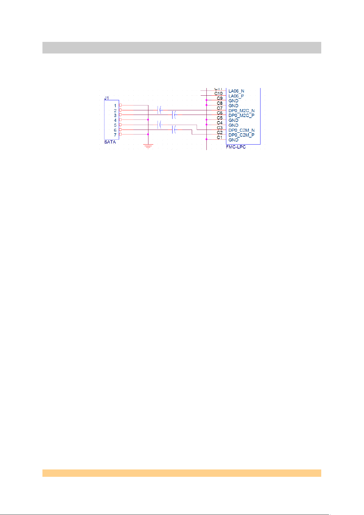
2 SATA
A SATA connector, J1, is provided that connects (via 100nF series capacitors) to the
FMC connector. The connectivity is shown here:
SMT SLB-FMC Issue 1.0 Page 7
Page 8

3 SLB / FMC Signals
C1
GND
C2
See SATA
C3
See SATA
C4
GND
C5
GND
C6
See SATA
C7
See SATA
C8
GND
C9
GND
C10
DOBQ4p / 98
C11
DOBQ4n / 100
C12
GND
C13
GND
C14
DOAQ2p / 89
C15
DOAQ2n / 91
C16
GND
C17
GND
C18
DOBQ0p / 82
C19
DOBQ0n / 84
C20
GND
C21
GND
C22
DOAI4p / 17
C23
DOAI4n / 19
C24
GND
C25
GND
C26
DOBI3p / 14
C27
DOBI3n / 16
C28
GND
C29
GND
C30
CNTRL3 / 48
C31
CNTRL1 / 47
C32
GND
C33
GND
C34
CNTRL0 / 45
C35
+12V
C36
GND
C37
+12V
C38
GND
C39
+3.3V
C40
GND
The majority of the signals are shown in the tables below. These list the FMC-LPC
pin reference together with the SLB pin name and number.
SMT SLB-FMC Issue 1.0 Page 8
Page 9

D1
10k Pull-up
D2
GND
D3
GND
D4
DOIRQp / 114
D5
DOIRQn / 116
D6
GND
D7
GND
D8
DOAQ4p / 97
D9
DOAQ4n / 99
D10
GND
D11
DOBQ5p / 102
D12
DOBQ5n / 104
D13
GND
D14
DOBQ3p / 94
D15
DOBQ3n / 96
D16
GND
D17
DOBQ1p / 86
D18
DOBQ1n / 88
D19
GND
D20
ClkOIp / 33
D21
ClkOIn / 35
D22
GND
D23
DOBI6p / 26
D24
DOBI6n / 28
D25
GND
D26
DOAI6p / 25
D27
DOAI6n / 27
D28
GND
D29
TCK
D30
TDI
D31
TDO
D32
+3.3V
D33
TMS
D34
TRST
D35
CNTRL2 / 46
D36
+3.3V
D37
GND
D38
+3.3V
D39
GND
D40
+3.3V
SMT SLB-FMC Issue 1.0 Page 9
Page 10

G1
GND
G2
ExTrgQp / 118
G3
ExTrgQn / 120
G4
GND
G5
GND
G6
ClkOQp / 113
G7
ClkOQn / 115
G8
GND
G9
DOBQ7p / 110
G10
DOBQ7n / 112
G11
GND
G12
DOAQ5p / 101
G13
DOAQ5n / 103
G14
GND
G15
DOAQ3p / 93
G16
DOAQ3n / 95
G17
GND
G18
DOAQ1p / 85
G19
DOAQ1n / 87
G20
GND
G21
DOBI7p / 30
G22
DOBI7n / 32
G23
GND
G24
DOBI5p / 22
G25
DOBI5n / 24
G26
GND
G27
DOAI5p / 21
G28
DOAI5n / 23
G29
GND
G30
DOBI2p / 10
G31
DOBI2n / 12
G32
GND
G33
DOBI1p / 6
G34
DOBI1n / 8
G35
GND
G36
DOBI0p / 2
G37
DOBI0n / 4
G38
GND
G39
VADJ
G40
GND
SMT SLB-FMC Issue 1.0 Page 10
Page 11

H1
NC H2
10k Pull-up
H3
GND
H4
RSLClkp / 117
H5
RSLClkn / 119
H6
GND
H7
DOAQ7p / 109
H8
DOAQ7n / 111
H9
GND
H10
DOAQ6p / 105
H11
DOAQ6n / 107
H12
GND
H13
DOBQ6p / 106
H14
DOBQ6n / 108
H15
GND
H16
DOBQ2p / 90
H17
DOBQ2n / 92
H18
GND
H19
DOAQ0p / 81
H20
DOAQ0n / 83
H21
GND
H22
DOBI4p / 18
H23
DOBI4n / 20
H24
GND
H25
DOAI7p / 29
H26
DOAI7n / 31
H27
GND
H28
DOAI3p / 13
H29
DOAI3n / 15
H30
GND
H31
DOAI2p / 9
H32
DOAI2n / 11
H33
GND
H34
DOAI1p / 5
H35
DOAI1n / 7
H36
GND
H37
DOAI0p / 1
H38
DOAI0n / 3
H39
GND
H40
VADJ
SMT SLB-FMC Issue 1.0 Page 11
Page 12

4 Circuit Diagram
Full circuit details can be obtained under NDA from Sundance.
SMT SLB-FMC Issue 1.0 Page 12
 Loading...