

Page 1

Sundance Multiprocessor Technology Limited
User Manual
Form : QCF42
Date : 11 February 2009
Unit / Module Description:
Dual ADC/DAC SLB Module
Unit / Module Number:
SMT943
Document Issue Number:
3
Issue Date:
23/06/2010
Original Author:
PhSR
Sundance Multiprocessor Technology Ltd, Chiltern House,
Waterside, Chesham, Bucks. HP5 1PS.
This document is the property of Sundance and may not be copied
nor communicated to a third party without prior written
permission.
© Sundance Multiprocessor Technology Limited 2009
User Manual
for
SMT943
User Manual SMT943 Last Edited: 23/08/2011 17:24:00
Page 2

Revision History
Issue
Changes Made
Date
Initials
1
Original document.
11/01/2010
PhSR
2
Update after testing v2.
19/06/2010
PhSR
3
Captures added.
23/06/2010
PhSR
User Manual SMT943 Page 2 of 54 Last Edited: 23/08/2011 17:24:00
Page 3

Table of Contents
Precautions ................................................................................................................................ 5
1 Introduction ..................................................................................................................... 6
2 Related Documents ........................................................................................................ 7
2.1 Referenced Documents .............................................................................................. 7
2.2 Applicable Documents ............................................................................................... 7
3 Functional Description .................................................................................................. 8
3.1 Block Diagram.............................................................................................................. 8
3.2 Module Description .................................................................................................... 8
3.2.1 A/D converters ....................................................................................................... 9
3.2.2 D/A converters ..................................................................................................... 12
3.2.3 Clock structure ..................................................................................................... 15
3.3 FPGA Design ............................................................................................................... 18
3.3.1 Control Register Settings .................................................................................... 18
Register Descriptions ......................................................................................................... 20
3.3.2 Control Register – 0x1. ........................................................................................ 20
CLOCK Register 0 – 0x10. .............................................................................................. 21
CLOCK Register 1 – 0x11. .............................................................................................. 22
CLOCK Register 2 – 0x12. .............................................................................................. 22
CLOCK Register 3 – 0x13. .............................................................................................. 23
CLOCK Register 4 – 0x14. .............................................................................................. 23
CLOCK Register 5 – 0x15. .............................................................................................. 24
CLOCK Register 6 – 0x16. .............................................................................................. 25
CLOCK Register 7 – 0x17. .............................................................................................. 25
CLOCK Register 8 – 0x18. .............................................................................................. 26
CLOCK Register 9 – 0x19. .............................................................................................. 26
CLOCK Register A – 0x1A. ............................................................................................. 27
CLOCK Register B – 0x1B. .............................................................................................. 27
CLOCK Register C – 0x1C. ............................................................................................. 28
CLOCK Register D – 0x1D. ............................................................................................. 28
CLOCK Register E – 0x1E. .............................................................................................. 29
CLOCK Register F – 0x1F. .............................................................................................. 29
CLOCK Register 10 – 0x20. ............................................................................................ 29
CLOCK Register 11 – 0x21. ............................................................................................ 30
CLOCK Register 12 – 0x22. ............................................................................................ 30
CLOCK Register 13 – 0x23. ............................................................................................ 31
CLOCK Register 14 – 0x24. ............................................................................................ 31
CLOCK Register 15 – 0x25. ............................................................................................ 32
CLOCK Register 16 – 0x26. ............................................................................................ 32
CLOCK Register 17 – 0x27. ............................................................................................ 33
CLOCK Register 18 – 0x28. ............................................................................................ 34
CLOCK Register 19 – 0x29. ............................................................................................ 34
ADC Chab Register 0 – 0x30. ........................................................................................ 35
User Manual SMT943 Page 3 of 54 Last Edited: 23/08/2011 17:24:00
Page 4

ADC Chab Register 1 – 0x31. ........................................................................................ 35
ADC Chab Register 2 – 0x32. ........................................................................................ 36
ADC Chab Register 3 – 0x33. ........................................................................................ 36
ADC Chab Register 4 – 0x34. ........................................................................................ 37
ADC Chab Register 5 – 0x35. ........................................................................................ 37
ADC Chab Register 6 – 0x36. ........................................................................................ 38
ADC Chab Register 7 – 0x37. ........................................................................................ 39
ADC Chab Register 8 – 0x38. ........................................................................................ 40
ADC Chab Register 9 – 0x39. ........................................................................................ 40
DAC chcd Register 0 – 0x40. ......................................................................................... 41
DAC chcd Register 1 – 0x41. ......................................................................................... 42
DAC chcd Register 2 – 0x42. ......................................................................................... 43
DAC chcd Register 3 – 0x43. ......................................................................................... 44
DAC chcd Register 4 – 0x44. ......................................................................................... 44
DAC chcd Register 5 – 0x45. ......................................................................................... 45
DAC chcd Register 6 – 0x46. ......................................................................................... 45
DAC chcd Register 7 – 0x47. ......................................................................................... 46
DAC chcd Register 8 – 0x48. ......................................................................................... 46
DAC chcd Register 9 – 0x49. ......................................................................................... 46
DAC chcd Register A – 0x4A. ........................................................................................ 47
DAC chcd Register B – 0x4B. ......................................................................................... 48
DAC chcd Register C – 0x4C. ........................................................................................ 48
DAC chcd Register D – 0x4D. ........................................................................................ 49
DAC chcd Register D – 0x4D. ........................................................................................ 49
DAC chcd Register E – 0x4E. ......................................................................................... 49
DAC Chcd – Phase shift DCM – 0x50. .......................................................................... 50
4 Pictures of the board ................................................................................................... 51
4.1 Top View ..................................................................................................................... 51
4.2 Bottom View ............................................................................................................... 52
5 Connectors ..................................................................................................................... 52
5.1 Description ................................................................................................................. 52
5.2 Location on the board .............................................................................................. 53
6 Physical Properties ....................................................................................................... 54
7 Safety ............................................................................................................................... 54
8 Ordering Information .................................................................................................. 54
9 EMC .................................................................................................................................. 54
User Manual SMT943 Page 4 of 54 Last Edited: 23/08/2011 17:24:00
Page 5

Table of Figures
Figure 1 - SMT943 Block diagram. .......................................................................................... 8
Figure 2 - ADC input terminated (50 Ohms). ..................................................................... 10
Figure 3 - ADC input terminated (50 Ohms) - Raw data. ................................................. 10
Figure 4 - ADCA input terminated (50 Ohm) - ADCB receiving a 20.04Mhz tone. ..... 11
Figure 5 – ADCA 20.6MHz tone - 200MSPS. ....................................................................... 11
Figure 6 - ADCA 60.55MHz tone - 200MSPS. ...................................................................... 12
Figure 7 - DAC Output 20.04-MHz sinewave - Narrow band. ......................................... 13
Figure 8 - DAC Output 20.04-MHz sinawave - Wide bandwidth. ................................... 14
Figure 9 - DAC output 20.04-MHz sinewave - Full bandwidth. ...................................... 14
Figure 10 - Clock Structure - Block Diagram ...................................................................... 15
Figure 11 - Clock Architecture Main Characteristics. ....................................................... 16
Figure 12 - External clock output (98.304MHz – Divided by 5 output) ........................ 16
Figure 13 - External Clock output (245.76MHz – Divided by 2 output). ....................... 17
Figure 14 - External Clock Output (491.52MHz – Divided by 1 output). ...................... 17
Figure 15 – Setup Packet Structure. ..................................................................................... 18
Figure 16 – Control Register Read Sequence. .................................................................... 18
Figure 17 – Register Memory Map. ....................................................................................... 19
Figure 18 - Connectors ........................................................................................................... 53
Figure 19 - SMT593 Loopback pcb. ...................................................................................... 54
Precautions
In order to guarantee that Sundance’s boards function correctly and to protect the
module from damage, the following precautions should be taken:
- They are static sensitive products and should be handled accordingly.
Always place the modules in a static protective bag during storage and transition.
User Manual SMT943 Page 5 of 54 Last Edited: 23/08/2011 17:24:00
Page 6

1 Introduction
The SMT943 is a single width expansion TIM that plugs onto an SLB base module,
the SMT351T (Virtex-5 LXT, SXT or even FXT FPGA) as an example and incorporates
1 Texas Instrument dual-channel Analog-to-Digital Converter (ADS62P49) and 1
Texas Instrument dual-channel Digital-to-Analog Converter (DAC5688). The SMT943
implements a comprehensive clock circuitry based on a chip (CDCE72010) from
Texas instrument that allows synchronisation among the converters and the use of
an external reference clock or sampling clock. It provides a complete conversion
solution and stands as a platform that can be part of a transmit/receive base
station. The SMT943 has an on-board VCXO of frequency 491.52MHz.
The DAC has a resolution of 16 bits and can update its outputs at up to
800MSamples per second. The converter is 1.8/3.3-Volt. Among the features of the
DAC5688 are integrated interpolation filters, a fine frequency mixer with a complex
NCO, a clock multiplier and IQ compensation. No DC-coupled version is currently
available on the DAC.
The ADC has a resolution of 14 bits and can update its outputs at up to 250MHz. All
converters are 1.8/3.3-Volt. ADCs internal gain and offset can be adjusted as well as
the data format. ADCs are AC-coupled on the board using a double-transformer
structure. No DC-coupled version is currently available on the ADC.
The Xilinx FPGA (Virtex-5 LXT or SXT series in the case of the SMT351T) on the base
module is responsible for handling data coming from one of the following sources:
Comports or Rocket Serial Link (RSL). These interfaces are compatible with a wide
range of Sundance’s modules.
The memory (DDR2) on the base module (still based on the case where using an
SMT351T SLB base module) can store samples.
Converter configuration, sampling and transferring modes are set via internal
control registers stored inside the FPGA and accessible via Comport.
The SMT943 module is well-suited for multi-carrier, wide bandwidth communication
applications.
The main features of the SMT943 are listed below:
● One Dual 14-bit 250MSPS ADC (ADS62P49),
● One Dual 16-bit 800MSPS DAC (DAC5688),
● On-board low-jitter clock distribution chip (CDCE72010),
● On-board 491.52MHz VCXO,
● On-board 10MHz reference crystal,
● One external clock, one external trigger and one reference clock inputs via
MMCX connector,
● One external clock output via MMCX connector,
● One SLB connector to link SMT943 and SMT351T (set to 2.5-V FPGA IOs) as
an example,
● All Analogue inputs to be connected to 50-Ohm sources.
● All Analogue outputs to be connected to 50-Ohm loads.
● A fan.
User Manual SMT943 Page 6 of 54 Last Edited: 23/08/2011 17:24:00
Page 7

2 Related Documents
2.1 Referenced Documents
ADC datasheet: Texas Instrument ADS62P49.
DAC datasheet: Texas Instrument DAC5688.
Clock datasheet: Texas Instrument CDCE72010.
2.2 Applicable Documents
User Manual SMT943 Last Edited: 23/08/2011 17:24:00
Page 8
SLB Interface connector
ADS62P49
Dual ADC Ch A
& Ch B
14-bit
250MSPS
(2x 675mW)
DAC5688
Dual channel
DAC
16-Bit
800MSPS
Interpolation
(1.3W)
Clock Synchronizer and
Jitter cleaner
Based on
CDCE72010
(1.8W)
Channel B
Signal
Conditioning
(AC coupling)
Channel A
Signal
Conditioning
(AC coupling)
Channel B
Signal
Conditioning
(AC coupling)
Channel A
Signal
Conditioning
(AC coupling)
DAC
Output
Ch A
MMCX
50 Ohm
DAC
Output
Ch B
MMCX
50 Ohm
ADC Input
Ch A
MMCX
50 Ohm
ADC Input
Ch B
MMCX
50 Ohm
ADCs
External
Clock in
MMCX
External
Refference
Clock in
MMCX
ADCs
External
Clock out
MMCX
Ch A – 1.8V DDR LVDS
Clock and Control
Ch B – 1.8V DDR LVDS
Clock and Control
Ch A – Data (16)
and Control
Ch B – Data (16)
and control
SLB Power connector
External Trigger
FPGA Clock
SMT943
ADC / DAC
Module, 2 ADC
Channels; 250MHz
@ 14 bits; 2 DACs
@ 800MHz/16 bits
Power Supplies:
1.8 and 3.3V
Linear
Regulators
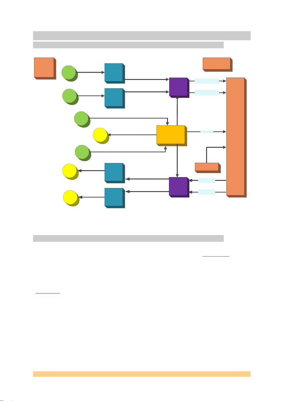
3 Functional Description
3.1 Block Diagram
Figure 1 - SMT943 Block diagram.
3.2 Module Description
The SMT943 has got 1 dual channel Analog-to-Digital converters (ADS62P49 – Texas
Instrument) that has been designed for multi-carrier, wide bandwidth
communication applications. Both analog inputs are available on MMCX connectors.
They are 50-Ohm AC-coupled inputs (RF transformers - ration 1). DDR LVDS lines
are used to carry samples through the SLB connector to the FPGA (SLB base module FPGA IOs must be set to 2.5-Volt). The module has also got a dual channel DAC
(DAC5688 – Texas Instrument) that has integrated 2x-8x interpolation filters, a fine
frequency mixer with a 32-bit complex numerically controlled oscillator, an onboard clock multiplier, an IQ compensation and an internal voltage reference.
A clock distribution chip ensures that all converters sample synchronously to a
single clock source. The clock source can be external or internal (on-board 491.52MHz VCXO). The distribution chip also allows synchronising the on-board VCXO to a
reference signal that can be external or internal (on-board 10-MHz crystal). External
reference, external sampling clock input and output are accessible on MMCX
connectors. An external trigger input is also available on the board.
All control, data and clock lines are mapped onto an SLB connector so the card can
be fully controlled by an SLB FPGA base module (SMT351T for example).
User Manual SMT943 Last Edited: 23/08/2011 17:24:00
Page 9
Some green LEDs are available on the board. A group of four LEDs is driven directly
Analogue Inputs
Input voltage range
0dB gain setting : 2.3Vpp - Full scale - AC
coupled
6dB gain setting : 1.15Vpp – Full Scale –
AC-coupled
Programmable input gain via register
(0…6dBs) by steps of 0.5dB (coarse gain)
and steps of 0.134dB (fine gain).
Impedance
Single-ended inputs – to be connected to a
50 source.
Bandwidth
Tbd – depends on ADC internal input gain.
ADC characteristics
Output Data Width per channel
14 Bits
Data Format
2’s Compliment or offset binary
(Changeable via control register)
SFDR
75 (0-db gain) / 82dBs (6-db gain)
maximum (manufacturer)
SNR
69 (0-db gain) / 66dBs (6-db gain)
maximum (manufacturer)
ENOB
11.3 bits maximum (manufacturer)
Maximum Sampling rate
250 MSPS
(1…100MSPS low speed mode)
(100…250MSPS high speed mode)
Minimum Sampling rate
1 MSPS
from the SLB base FPGA module and can be used to return status bits. Other
indivudual LEDs should be lit and show that local power supplies are on.
3.2.1 A/D converters
The main characteristics of the SMT943 are gathered into the following table.
ADC Analog inputs on the board are single-ended. A double RF transformer
structure is used to provide single-ended to differential conversion. Both
transformers are identical and have a ratio of 1. In order to match the 50-Ohm at
the connector, the output of the second transformer has two 25-Ohm resistors
terminated to the ADC common mode voltage.
Below are some captures. All of them are 2048 points. ADCs are sampling at
245.76MHz and have an input gain of 6dBs:
User Manual SMT943 Page 9 of 54 Last Edited: 23/08/2011 17:24:00
Page 10
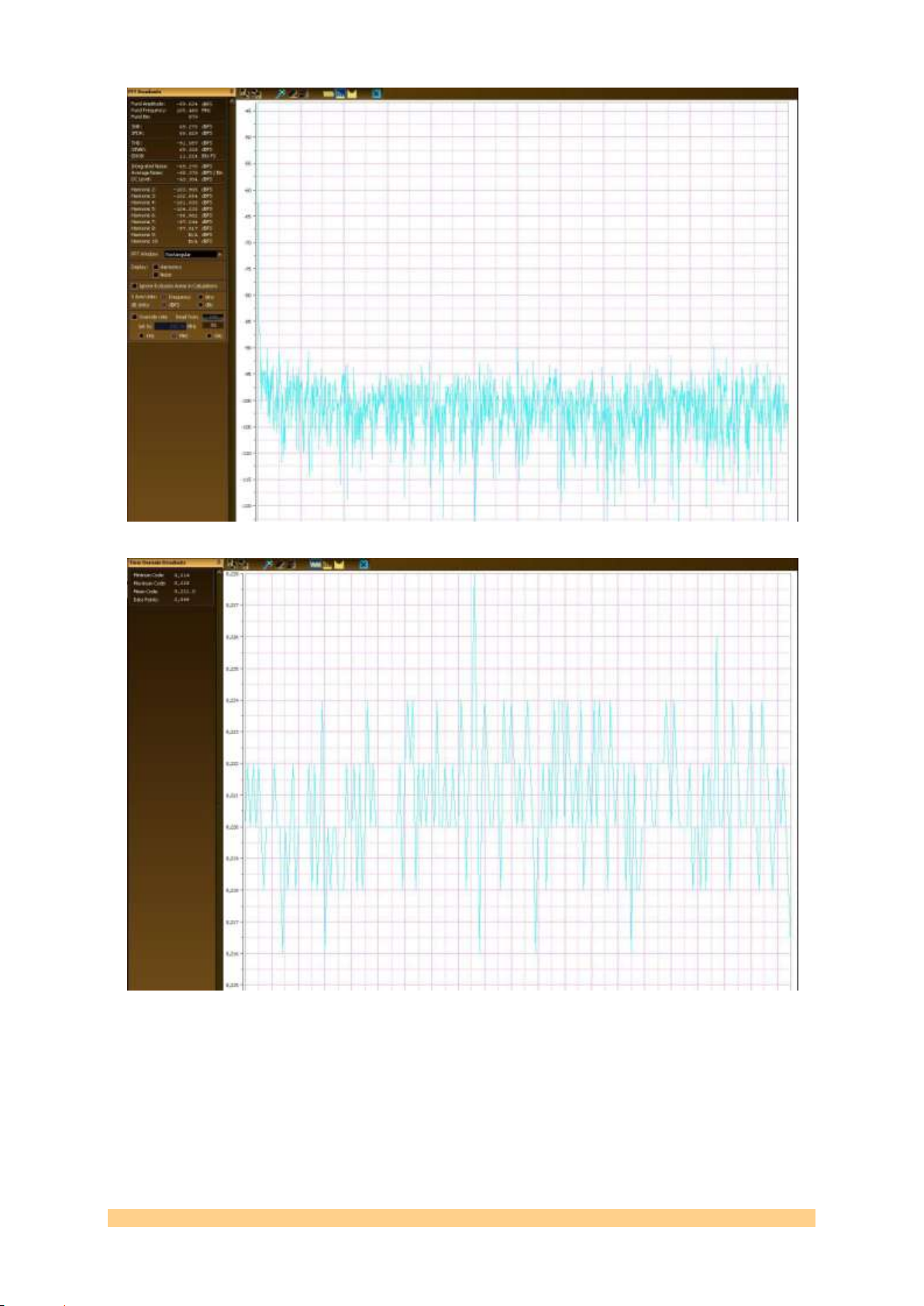
Figure 2 - ADC input terminated (50 Ohms).
Figure 3 - ADC input terminated (50 Ohms) - Raw data.
User Manual SMT943 Page 10 of 54 Last Edited: 23/08/2011 17:24:00
Page 11
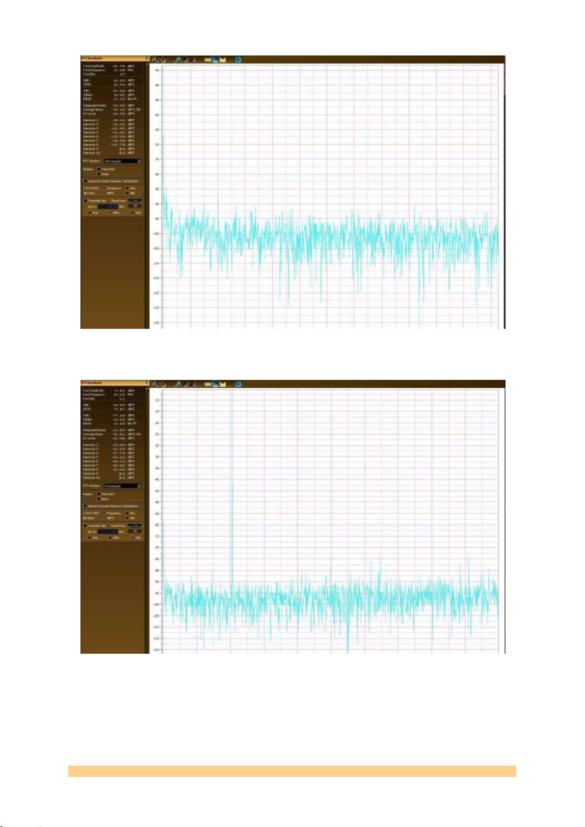
Figure 4 - ADCA input terminated (50 Ohm) - ADCB receiving a 20.04Mhz tone.
Below are some captures. All are 2048 points. ADCs are sampling at 200MHz and
have an input gain of 6dBs:
Figure 5 – ADCA 20.6MHz tone - 200MSPS.
User Manual SMT943 Page 11 of 54 Last Edited: 23/08/2011 17:24:00
Page 12
Figure 6 - ADCA 60.55MHz tone - 200MSPS.
Analogue Outputs
Output voltage range
1 Vp-p – Full scale - AC coupled
Impedance
DAC single-ended outputs are to be
connected to a 50 load, which impedance
matching implemented between DAC and
RF transformers.
SFDR
89dBs maximum (manufacturer)
SNR
80dBs maximum (manufacturer)
Bandwidth
TBD
DAC Input
Output Data Width per channel
16-Bits
Data Format
2’s Compliment or offset binary
(Changeable via control register)
SFDR
85dBs maximum (manufacturer)
SNR
73dBs maximum (manufacturer)
Maximum input data rate
250 MSPS (Clk1 – DAC5688)
Maximum Sampling rate
800 MSPS (Clk2 – DAC5688)
3.2.2 D/A converters
The main characteristics of the SMT943 are gathered into the following table.
User Manual SMT943 Page 12 of 54 Last Edited: 23/08/2011 17:24:00
Page 13
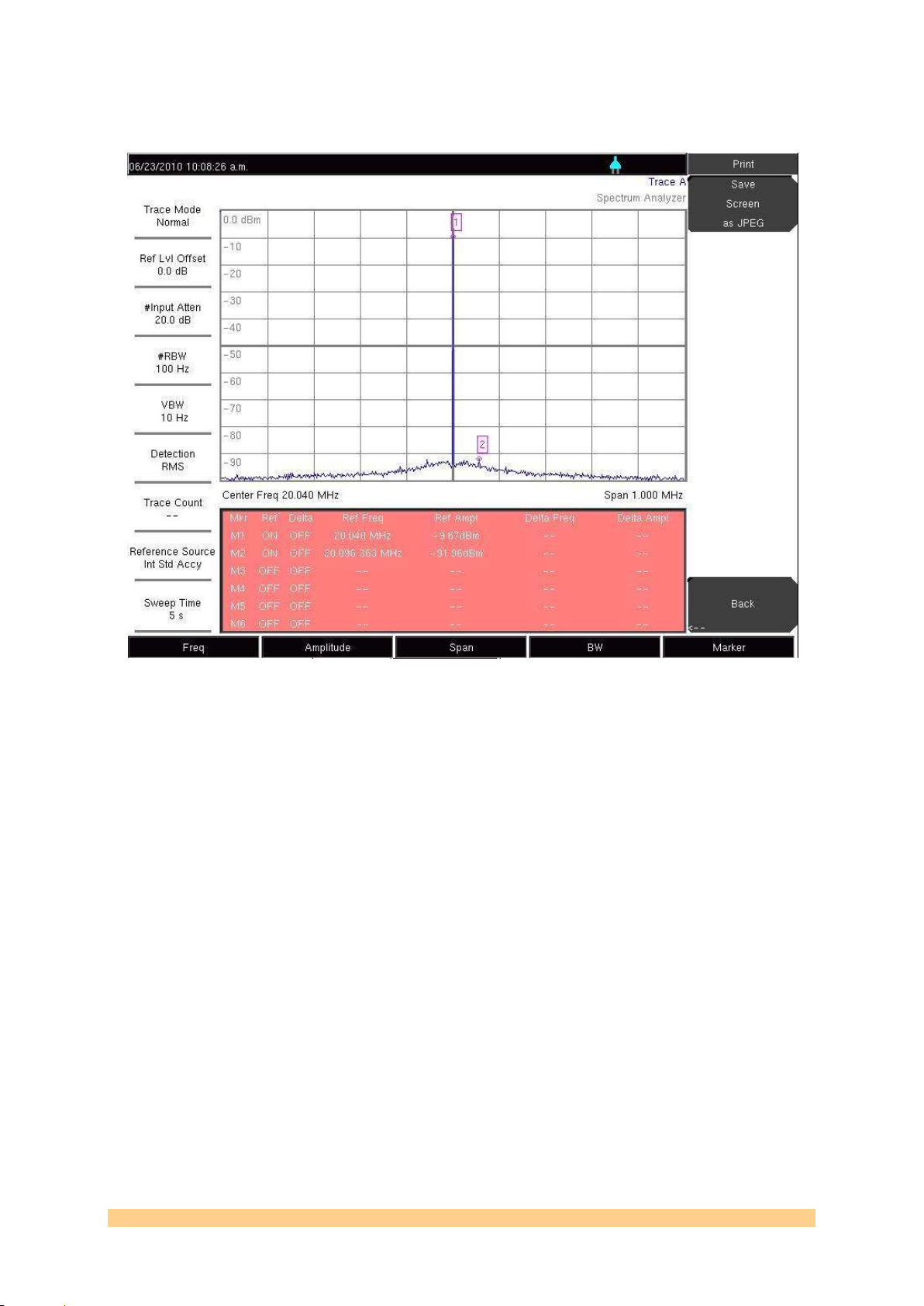
Below are some captures of the DAC output. The DAC was set to output a 20.04MHz tone under a sampling clock of 245.76MHz and an interpolation factor of 2
(DAC internally clocked at 491.52MHz):
Figure 7 - DAC Output 20.04-MHz sinewave - Narrow band.
User Manual SMT943 Page 13 of 54 Last Edited: 23/08/2011 17:24:00
Page 14
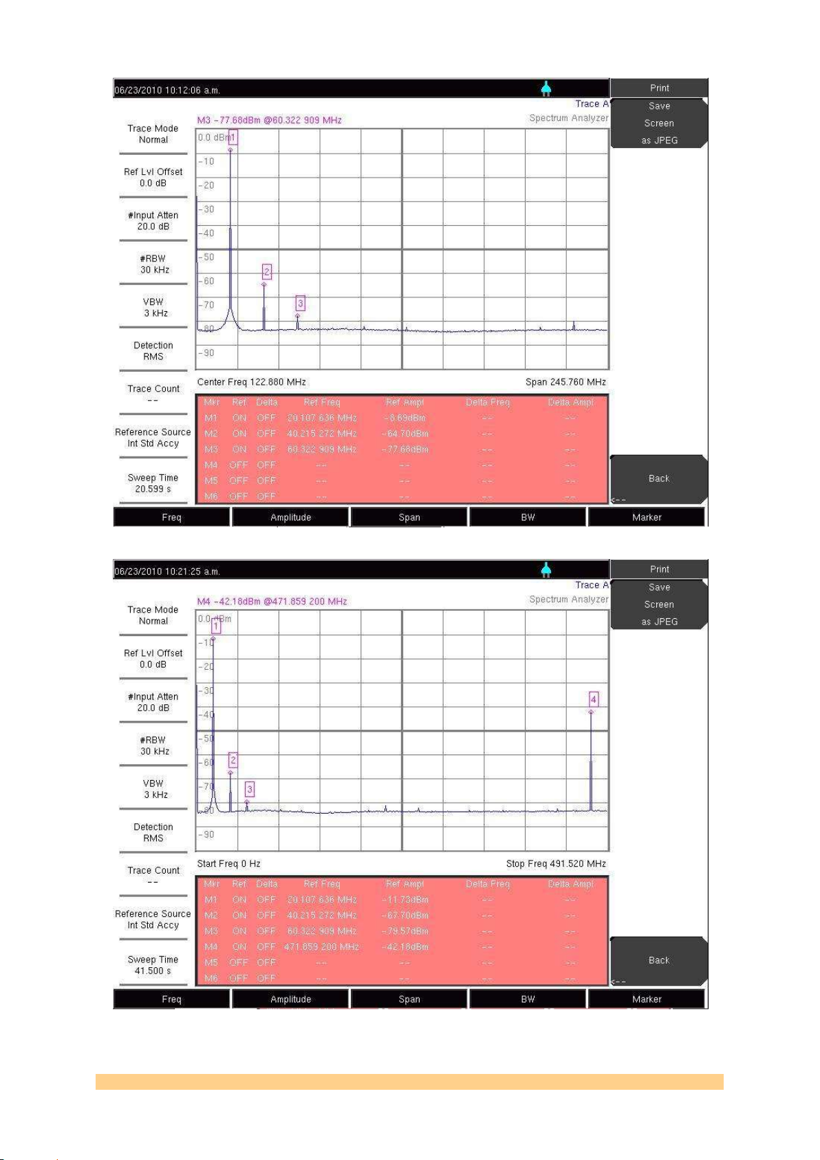
Figure 8 - DAC Output 20.04-MHz sinawave - Wide bandwidth.
Figure 9 - DAC output 20.04-MHz sinewave - Full bandwidth.
User Manual SMT943 Page 14 of 54 Last Edited: 23/08/2011 17:24:00
Page 15
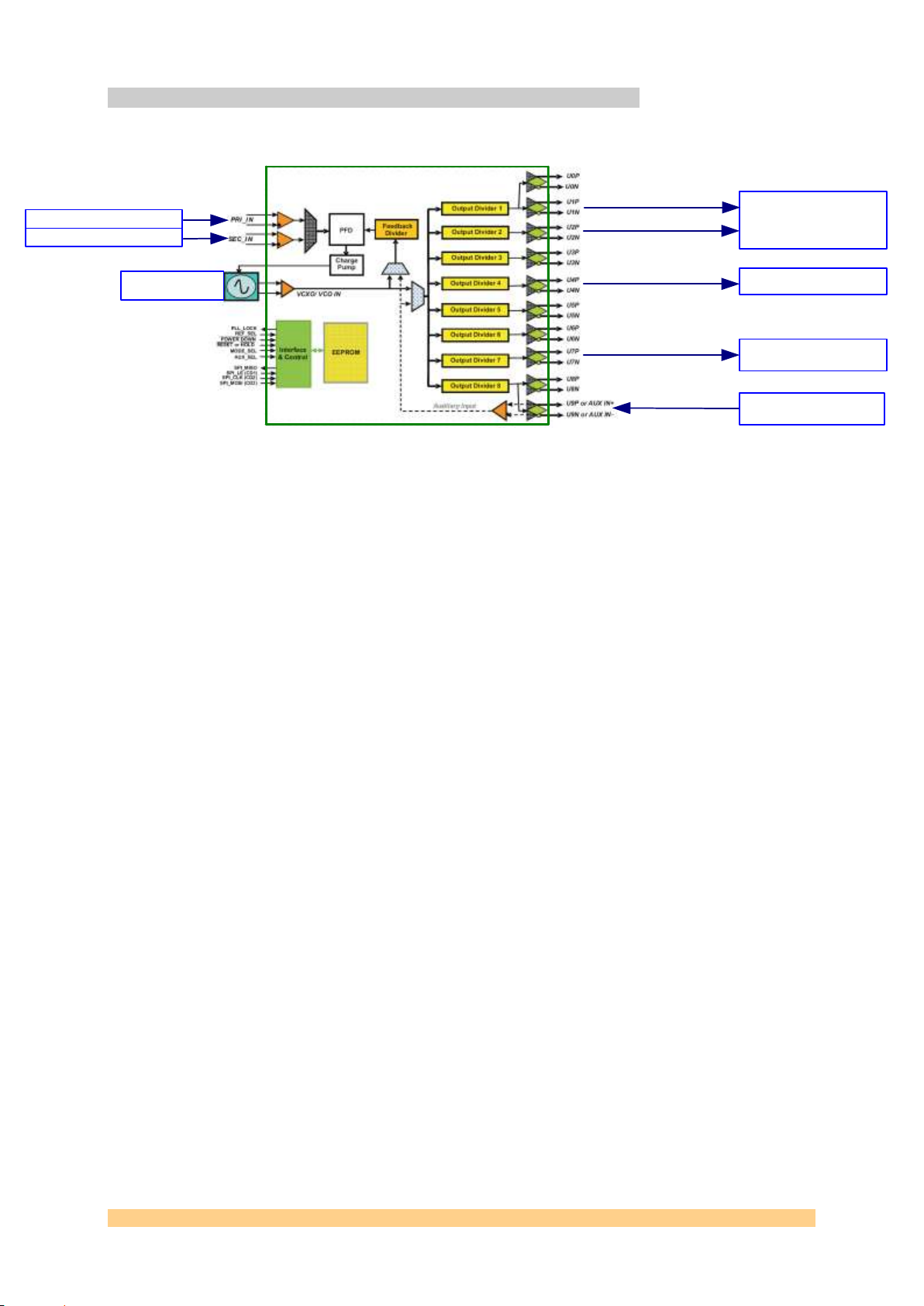
3.2.3 Clock structure
Clock Synthesizer and Jitter Cleaner - Texas Instrument CDCE72010
U2 - DAC Clk2 Channel c&d
U7 - Clk Out and FPGA Clk Output (ExtClkOut)
FPGA (SLB)
Clk In
Clk Input (ExtClkIn)
On-board VCXO
491.52 MHz
On-board 10-MHz reference
External Reference (ExtRefIn)
DAC Chc&d – DAC5688
16-bit 800MSPS
U4 - ADC Channel a&b
ADC Cha&b – ADS62P49
14-bit 250MSPS
U1 - DAC Clk1 Channel c&d
The following diagram shows the clock structure of the SMT943:
Figure 10 - Clock Structure - Block Diagram
The clock distribution chip used on the SMT943 offers 2 reference inputs, a VCXO
differential input and a charge pump to drive the VCXO, as well as a second
differential clock input. ADCs, DACs and external clock are mapped to separate
internal output dividers in order to give more flexibility.
The CDCE72010 chip is designed to provide clean, phase related clocks to the
converters. The reference clock (on-board or external) is used to lock the on-board
VCXO using the clock chip PLL/charge pump. It is also possible to feed an external
sampling clock to the chip that can then be distributed the analog converters.
Note that when the board is mounted onto a PXI SLB carrier such as the SMT700
(with 2.5-Volt FPGA IOs), it is possible to feed the 10-MHz reference clock (PXI bus)
to the SMT943 order to lock the VCXO, then creating a local source synchronised to
the rest of the system.
Also to be noted is that a VCXO of a different frequency can be fitted to replace the
standard 800-MHz one. It is to be discussed prior to ordering as it is an operation
carried out in the factory.
User Manual SMT943 Page 15 of 54 Last Edited: 23/08/2011 17:24:00
Page 16
The table below gathers the characteristics of all clock inputs/outputs:
External Reference Input
Input Voltage Level
1 – 3.3 Volts peak-to-peak (AC-coupled)
Frequency Range
0 – 100 MHz.
External Sampling Clock Input
Input Voltage Level
1.5 – 3.3 Volts peak-to-peak (AC-coupled)
Input Format
Single-ended.
Frequency range
10-500 MHz
External Sampling Clock Output
Output Voltage Level
0-2.4 Volts fixed amplitude
Output Format
LVTTL
External Trigger Inputs
Input Voltage Level
1.2-2.5 Volts peak-to-peak.
Format
DC-coupled and Single-ended. Protected by 2
clamping diodes.
Format
LVCMOS
Figure 11 - Clock Architecture Main Characteristics.
Below are shown some captures of the external clock output:
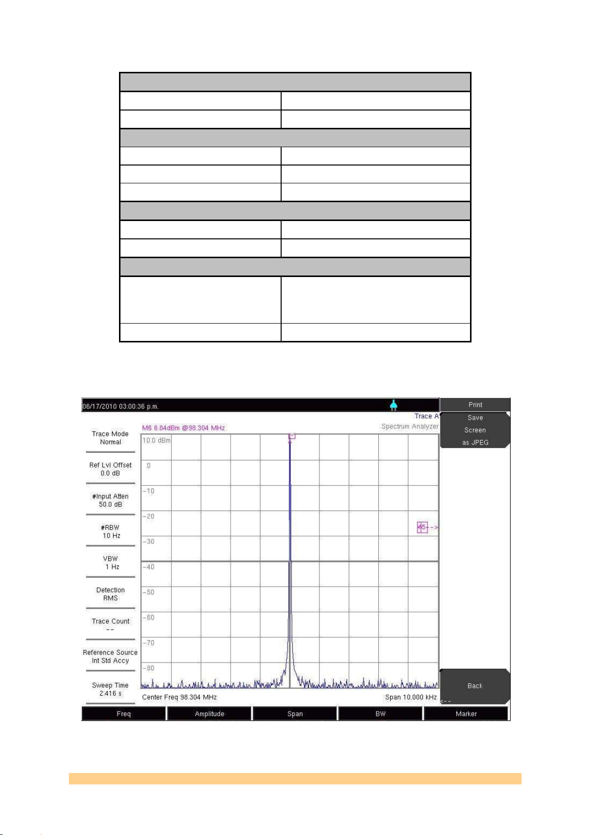
Figure 12 - External clock output (98.304MHz – Divided by 5 output)
User Manual SMT943 Page 16 of 54 Last Edited: 23/08/2011 17:24:00
Page 17
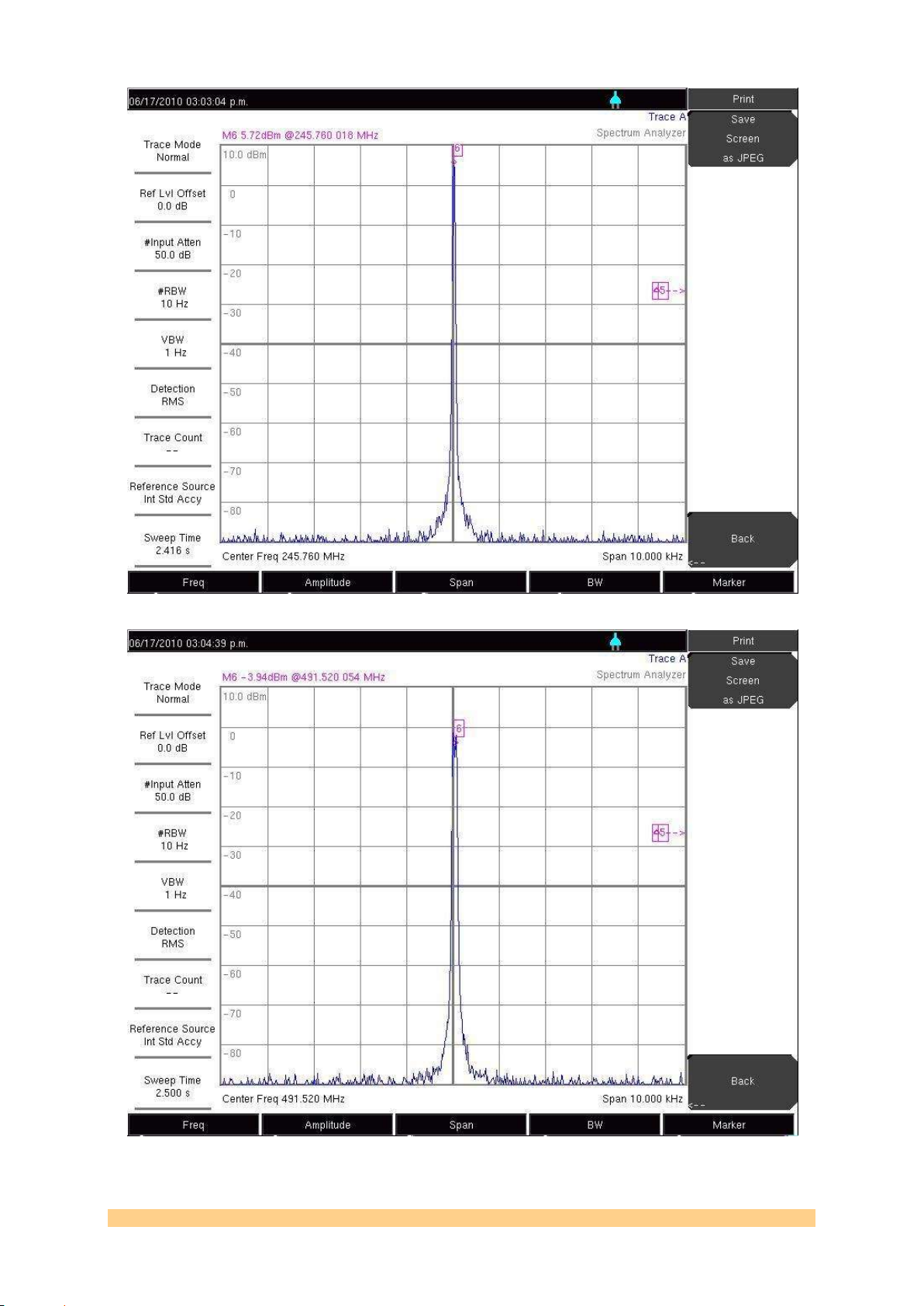
Figure 13 - External Clock output (245.76MHz – Divided by 2 output).
Figure 14 - External Clock Output (491.52MHz – Divided by 1 output).
User Manual SMT943 Page 17 of 54 Last Edited: 23/08/2011 17:24:00
Page 18

3.3 FPGA Design
Byte Content
Byte
Bit 7
Bit 6
Bit 5
Bit 4
Bit 3
Bit 2
Bit 1
Bit 0
3
Command
3
Command
2
Command
1
Command
0
Address
11
Address
10
Address 9
Address 8
2
Address 7
Address 6
Address 5
Address 4
Address 3
Address 2
Address 1
Address 0
1
Data 15
Data 14
Data 13
Data 12
Data 11
Data 10
Data 9
Data 8
0
Data 7
Data 6
Data 5
Data 4
Data 3
Data 2
Data 1
Data 0
Host
Fixed Sequence
SMT942
ComPort 3
Byte 0
Read/Write AddressByte 1
Read/Write DataByte 3
Read/Write DataByte 4
1) Write Packet
The standard FPGA design implements all the registers described in the followings
parts.
3.3.1 Control Register Settings
The Control Registers control the complete functionality of the SMT943. They are
setup via the Comport3 (standard firmware provided). The settings of the
ADCs/DACs, triggers, clocks and the configuration of the interfaces and the internal
FPGA data path settings can be configured via the Control Registers.
3.3.1.1 Control Packet Structure
The data passed on to the SMT943 over the Comport must conform to a certain
packet structure. Only valid packets will be accepted and only after acceptance of a
packet will the appropriate settings be implemented. Each packet will start with a
command (4 bits – 0x1 for a write operation – 0x2 for a read operation) information,
followed by a register address (12 bits – see table Memory Map), followed by a 16-bit
data. This structure is illustrated in the following figure:
Figure 15 – Setup Packet Structure.
3.3.1.2 Reading and Writing Registers
Control packets are sent to the SMT943 over Comport3. This is a bi-directional
interface. The format of a ‘Read Packet’ is the same as that of a write packet.
Figure 16 – Control Register Read Sequence.
User Manual SMT943 Page 18 of 54 Last Edited: 23/08/2011 17:24:00
Page 19

3.3.1.3 Memory Map
Address
Writable Registers
Readable Registers
0x00
Reserved.
Reserved.
0x01
Board Control Register.
Firmware Version.
0x02
Reserved.
Clock Readback Register.
0x03
Reserved.
Board Status Register
Clock Section
0x10
Clock Register 0x0.
Read-back (FPGA Register) Clock Register 0x0.
0x11
Clock Register 0x1.
Read-back (FPGA Register) Clock Register 0x1.
…
…
0x28
Clock Register 0x18.
Read-back (FPGA Register) Clock Register 0x18.
0x29
Clock Register 0x19.
Read-back (FPGA Register) Clock Register 0x19.
0x2A
Clock Readback Address Register (LSB)
0x2B
Clock Readback Address Register (MSB)
ADCab Section
0x30
ADCab Register 0x0.
Read-back (FPGA Register) ADCab Register 0x0.
0x31
ADCab Register 0x1.
Read-back (FPGA Register) ADCab Register 0x1.
…
...
0x3D
ADCab Register 0x8.
Read-back (FPGA Register) ADCab Register 0x8.
0x3E
ADCab Register 0x9.
Read-back (FPGA Register) ADCab Register 0x9.
DACcd Section
0x40
DACcd Register 0x0.
Read-back (FPGA Register) DACcd Register 0x0.
0x41
DACcd Register 0x1.
Read-back (FPGA Register) DACcd Register 0x1.
…
...
0x4D
DACcd Register 0xD.
Read-back (FPGA Register) DACcd Register 0xD.
0x4E
DACcd Register 0xE.
Read-back (FPGA Register) DACcd Register 0xE.
DACcd DCM Section
0x50
DCM DAC chc&d Phase shift.
Reserved
The write packets must contain the address where the data must be written to and
the read packets must contain the address where the required data must be read.
The following figure shows the memory map for the writable and readable Control
Registers on the SMT943:
User Manual SMT943 Page 19 of 54 Last Edited: 23/08/2011 17:24:00
Figure 17 – Register Memory Map.
Page 20

Register Descriptions
Control Register 0x01
Byte
Bit 7
Bit 6
Bit 5
Bit 4
Bit 3
Bit 2
Bit 1
Bit 0
1
Sync (chcd)
TxEnable
(chcd)
Trigger
nled
(chcd)
Trigger
nled
(chab)
DCM chcd
reset
DCM chab
reset
Clk_Readb
ack
Default
0
Chcd
trigger
selection
Chdc
internal
trigger
Chab
trigger
selectio
n
Chab
internal
trigger
Chab
Reset
Chcd
update
Chab
update
clk update
Default
‘0’
‘0’
‘0’
‘0’
‘0’
‘0’
‘0’
‘0’
Clock Register 0 0x10
Setting
Bit 0
Description clk update clock chip register update
0
0
No action.
1
1
All clock registers are sent to the clock chip via its serial interface.
Setting
Bit 1
Description chab update channel a and b register update
0
0
No action.
1
1
All registers (chab) are sent to the converter via its serial interface.
Setting
Bit 2
Description chcd update channel c and d register update
0
1
No action.
1
1
All registers (chcd) are sent to the converter via its serial interface.
Setting
Bit 4
Description chab Internal trigger
0
0
No action.
1
1
Starts the data flow (converter chab).
Setting
Bit 5
Description chab trigger selection
0
0
Trigger from control register selected.
1
1
Trigger from external source selected.
Setting
Bit 6
Description chcd Internal trigger
0
0
No action.
1
1
Starts the data flow (converter chcd).
Setting
Bit 7
Description chcd trigger selection
0
0
Trigger from control register selected.
1
1
Trigger from external source selected.
Setting
Bit 8
Description clock readback
0
0
No action.
1
1
Used when read register back from the chip itself.
Setting
Bit 9
Description DCM chab Reset
0
0
No action.
1
1
Resets the DCM used to capture samples from ADC channels.
Setting
Bit 10
Description DCM chcd Reset
3.3.2 Control Register 0x1.
User Manual SMT943 Page 20 of 54 Last Edited: 23/08/2011 17:24:00
Page 21

0
0
No action.
1
1
Resets the DCM used to send samples to DAC channels.
Setting
Bit 11
Description Trigger/nLed
0
0
Led13 flashes at a divided version of the ADCs clock.
1
1
Led13 shows the state of chab trigger. (on=trigger active)
Setting
Bit 12
Description Trigger/nLed
0
0
Led12 flashes at a divided version of the DACs clock.
1
1
Led12 shows the state of chcd trigger. (on=trigger active)
Setting
Bit 14
Description Tx-enable (chcd)
0
0
Precvents samples to reach the DAC (chcd)
1
1
Allows samples to reach the DAC (chcd)
Setting
Bit 15
Description synch (chcd)
0
0 1
1
Clock Register 0 0x10
Byte
Bit 7
Bit 6
Bit 5
Bit 4
Bit 3
Bit 2
Bit 1
Bit 0
1
Reserved
Reserved
CP_DIR
CP_MODE
DELAY_PFD
REFSELCNTRL
VCXO_AUX_SEL
Default
‘0’
‘0’
‘0’
‘0’
‘00’
‘0’
‘0’
0
SECSEL_PRISEL
Reserved
Reserved
Default
‘00’
‘00’
‘0000’
Clock Register 0 0x10
Setting
Bit 7:6
Description SECSEL_PRISEL Reference Input Selection
0
00
Nothing Selected
1
01
On-board Reference selected
2
10
External Reference selected
3
11
Auto Selection (Not recommended)
Setting
Bit 8
Description VCXO_AUX_SEL VCXO/AUX Selection
0
0
On-board or External Reference. Selected (SECSEL_PRI_SEL)
1
1
On-board VCXO or External Clock selected.
Setting
Bit 9
Description REFSELCNTRL Reference selection mode
0
0
Reference selection made externally.
1
1
Reference selection made internally (using SECSEL_PRISEL.).
Setting
Bit 11:10
Description DELAY_PFD PFD pulse width
0
00
LED14 shows the lock status of the DCM used to collect samples from the ADC
channels. The DCM is locked when the LED is ON.
LED11 shows the lock status of the DCM used to send samples to the DAC channels.
The DCM is locked when the LED is ON.
CLOCK Register 0 0x10.
User Manual SMT943 Page 21 of 54 Last Edited: 23/08/2011 17:24:00
Page 22

1
01
2 10
3 11
Setting
Bit 12
Description CP_MODE
0
0
3V. 1 1
5V
Setting
Bit 13
Description CP_DIR
0
0
Positive CP current output
1
1
Negative CP current output
Clock Register 1 0x11
Byte
Bit 7
Bit 6
Bit 5
Bit 4
Bit 3
Bit 2
Bit 1
Bit 0
1
Output0 (DAC chc&d clk1) Mode
PECLOHISWING
Reserved
Default
‘100000’
‘0’
‘0’ 0 Reserved
ICP
CP_PRE
Reserved
Default
‘00’
‘0000’
‘0’
‘0’
Reset Register 1 0x11
Setting
Bit 1
Description CP_PRE - Preset charge pump output voltage to vcc/2
0
0
OFF. 1 1
ON.
Setting
Bit 5:2
Description ICP Charge pump current setting
0
0
1 1
Setting
Bit 9
Description PECL0HISWING PECL output voltage swing (DAC chc&d clk1)
0
0
Normal Operation.
1
1
High PECL output voltage.
Setting
Bit 15:10
Description Output0 (DAC chc&d clk1) mode
0
0
LVPECL only: ‘100000’.
Clock Register 2 0x12
Byte
Bit 7
Bit 6
Bit 5
Bit 4
Bit 3
Bit 2
Bit 1
Bit 0
1
Coarse Phase Adjustment[5:0] (Output DAC chc&d clk1 and clk2)
Reserved
Default
‘000000’
‘00’
0
Reserved
Reserved
Default
‘0011’
‘0001’
CLOCK Register 1 0x11.
CLOCK Register 2 0x12.
User Manual SMT943 Page 22 of 54 Last Edited: 23/08/2011 17:24:00
Page 23

Reset Register 2 0x12
Setting
Bit 15:10
Description Coarse Phase Adjustment[5:0] DAC chc&d clk1 and clk2
0
0
1 1
Clock Register 3 0x13
Byte
Bit 7
Bit 6
Bit 5
Bit 4
Bit 3
Bit 2
Bit 1
Bit 0
1
Output0 (DAC chc&d clk2) Mode
PECL1HISWING
Output
Divider
Enable
Default
‘100000’
‘0’
‘0’
0
Output Divider Ratio DAC chc&d clk1 and clk2
Coarse Phase
Adjustment[6]
Default
‘0000000’
‘0’
Reset Register 3 0x13
Setting
Bit 0
Description - Coarse Phase Adjustment[6] DAC chc&d clk1 and clk2
0
0
1 1
Setting
Bit 7:1
Description Output Divider Ratio DAC chc&d clk1 and clk2
0
0
1 1
Setting
Bit 8
Description Output Divider Enable DAC chc&d clk1 and clk2
0
0
Divider disabled.
1
1
Divider enabled.
Setting
Bit 9
Description PECL1HISWING PECL output voltage swing (DAC chc&d clk2)
0
0
Normal Operation.
1
1
High PECL output voltage.
Setting
Bit 15:10
Description Output1 (DAC chc&d clk2) mode
0
0
LVPECL only: ‘100000’.
Clock Register 4 0x14
Byte
Bit 7
Bit 6
Bit 5
Bit 4
Bit 3
Bit 2
Bit 1
Bit 0
1
Coarse Phase Adjustment[5:0] (Output DAC cha&b clk1)
Delay N[2:1]
Default
‘000000’
‘00’
0
Delay N[0]
Delay M
Reserved
Default
‘0’
‘0’
‘0010’
CLOCK Register 3 0x13.
CLOCK Register 4 0x14.
User Manual SMT943 Page 23 of 54 Last Edited: 23/08/2011 17:24:00
Page 24

Reset Register 4 0x14
Setting
Bit 6:4
Description Delay M
0
0
1 1
Setting
Bit 9:7
Description Delay N
0
0
1 1
Setting
Bit 15:10
Description Coarse Phase Adjustment[5:0] DAC cha&b clk1
0
0
1 1
Clock Register 5 0x15
Byte
Bit 7
Bit 6
Bit 5
Bit 4
Bit 3
Bit 2
Bit 1
Bit 0
1
Output0 (DAC cha&b clk1) Mode
PECL2HISWING
Output
Divider
Enable
Default
‘100000’
‘0’
‘0’
0
Output Divider Ratio DAC cha&b clk1
Coarse Phase
Adjustment[6]
Default
‘0000000’
‘0’
Reset Register 5 0x15
Setting
Bit 0
Description - Coarse Phase Adjustment[6] DAC cha&b clk1
0
0
1 1
Setting
Bit 7:1
Description Output Divider Ratio DAC cha&b clk1
0
0
1 1
Setting
Bit 8
Description Output Divider Enable DAC cha&b clk1
0
0
Divider disabled.
1
1
Divider enabled.
Setting
Bit 9
Description PECL2HISWING PECL output voltage swing (DAC cha&b clk1)
0
0
Normal Operation.
1
1
High PECL output voltage.
Setting
Bit 15:10
Description Output2 (DAC cha&b clk1) mode
0
0
LVPECL only: ‘100000’.
CLOCK Register 5 0x15.
User Manual SMT943 Page 24 of 54 Last Edited: 23/08/2011 17:24:00
Page 25

CLOCK Register 6 0x16.
Clock Register 6 0x16
Byte
Bit 7
Bit 6
Bit 5
Bit 4
Bit 3
Bit 2
Bit 1
Bit 0
1
Coarse Phase Adjustment[5:0] (Output DAC cha&b clk2)
BIAS_DIV23
Default
‘000000’
‘00’
0
BIAS_DIV01
Reserved
DIS_FDET_REF
Reserved
Default
‘00’
‘0’
‘0’
‘0011’
Reset Register 6 0x16
Setting
Bit 4
Description DIS_FDET_REF
0
0
Reference Clock detector is ON
1
1
Reference Clock detector is OFF
Setting
Bit 7:6
Description BIAS_DIV01 Current reduction output dividers 0 and 1
0
‘00’
No current output reduction
1
‘01’
20% output current reduction
2
‘10’
30% output current reduction
Setting
Bit 9:8
Description BIAS_DIV23 Current reduction output dividers 2 and 3
0
‘00’
No current output reduction
1
‘01’
20% output current reduction
2
‘10’
30% output current reduction
Setting
Bit 15:10
Description Coarse Phase Adjustment[5:0] DAC cha&b clk1
0
0
1 1
Clock Register 7 0x17
Byte
Bit 7
Bit 6
Bit 5
Bit 4
Bit 3
Bit 2
Bit 1
Bit 0
1
Output0 (DAC cha&b clk2) Mode
PECL3HISWING
Output
Divider
Enable
Default
‘100000’
‘0’
‘0’
0
Output Divider Ratio DAC cha&b clk1 and clk2
Coarse Phase
Adjustment[6]
Default
‘0000000’
‘0’
Reset Register 7 0x17
Setting
Bit 0
Description - Coarse Phase Adjustment[6] DAC cha&b clk2
0
0
1 1
Setting
Bit 7:1
Description Output Divider Ratio DAC cha&b clk2
0
0
CLOCK Register 7 0x17.
User Manual SMT943 Page 25 of 54 Last Edited: 23/08/2011 17:24:00
Page 26

1
1
Setting
Bit 8
Description Output Divider Enable DAC cha&b clk2
0
0
Divider disabled.
1
1
Divider enabled.
Setting
Bit 9
Description PECL3HISWING PECL output voltage swing (DAC cha&b clk2)
0
0
Normal Operation.
1
1
High PECL output voltage.
Setting
Bit 15:10
Description Output3 (DAC cha&b clk2) mode
0
0
LVPECL only: ‘100000’.
Clock Register 8 0x18
Byte
Bit 7
Bit 6
Bit 5
Bit 4
Bit 3
Bit 2
Bit 1
Bit 0
1
Coarse Phase Adjustment[5:0] (External Clock)
Reserved
HOLD_ON_LOR
Default
‘000000’
‘0’
‘0’
0
Reserved
Reserved
Default
‘0000’
‘0011’
Reset Register 8 0x18
Setting
Bit 8
Description HOLD_ON_LOR
0
0
Normal mode of operation
1
1
Charge pump in tri-state mode
Setting
Bit 15:10
Description Coarse Phase Adjustment[5:0] External Clock
0
0
1 1
Clock Register 9 0x19
Byte
Bit 7
Bit 6
Bit 5
Bit 4
Bit 3
Bit 2
Bit 1
Bit 0
1
Output0 (External Clock) Mode
PECL4HISWING
Output
Divider
Enable
Default
‘100000’
‘0’
‘0’
0
Output Divider Ratio External Clock
Coarse Phase
Adjustment[6]
Default
‘0000000’
‘0’
CLOCK Register 8 0x18.
CLOCK Register 9 0x19.
User Manual SMT943 Page 26 of 54 Last Edited: 23/08/2011 17:24:00
Page 27

Reset Register 9 0x19
Setting
Bit 0
Description - Coarse Phase Adjustment[6] External Clock
0
0
1 1
Setting
Bit 7:1
Description Output Divider Ratio External Clock
0
0
1 1
Setting
Bit 8
Description Output Divider Enable External Clock
0
0
Divider disabled.
1
1
Divider enabled.
Setting
Bit 9
Description PECL4HISWING PECL output voltage swing (External Clock)
0
0
Normal Operation.
1
1
High PECL output voltage.
Setting
Bit 15:10
Description Output4 (External Clock) mode
0
0
LVPECL only: ‘100000’.
Clock Register A 0x1A
Byte
Bit 7
Bit 6
Bit 5
Bit 4
Bit 3
Bit 2
Bit 1
Bit 0
1
Reserved
Reserved
Default
‘000000’
‘00’
0
Reserved
BIAS_DIV45
Reserved
Default
‘00’
‘00’
‘0101’
Reset Register A 0x1A
Setting
Bit 5:4
Description BIAS_DIV01 Current reduction output dividers 0 and 1
0
‘00’
No current output reduction
1
‘01’
20% output current reduction
2
‘10’
30% output current reduction
Clock Register B 0x1B
Byte
Bit 7
Bit 6
Bit 5
Bit 4
Bit 3
Bit 2
Bit 1
Bit 0
1
Reserved
Default
‘01101000’
0
Reserved
Default
‘00000000’
CLOCK Register A 0x1A.
CLOCK Register B 0x1B.
User Manual SMT943 Page 27 of 54 Last Edited: 23/08/2011 17:24:00
Page 28

CLOCK Register C 0x1C.
Clock Register C 0x1C
Byte
Bit 7
Bit 6
Bit 5
Bit 4
Bit 3 Bit 2
Bit 1
Bit 0
1
Reserved
DET_STAR
T_BYPASS
FB_START
_BYPASS
Default
‘000000’
‘0’
‘0’
0
DIV2_DIS
DIV_SEL
Reserve
d
FB_FD_DESEL
Reserved
Default
‘0’
‘0’
‘0’
‘0’
‘0110’
Reset Register C 0x1C
Setting
Bit 4
Description FB_FD_DESEL
0
‘0’
Feedback frequency detector is connected to the lock detector
1
‘1’
Feedback frequency detector is disconnected from the lock detector
Setting
Bit 6
Description DIV_SEL
0
‘0’
FB Clock divided by 1
1
‘1’
FB Clock divided by 2
Setting
Bit 7
Description DIV2_DIS
0
‘0’
Normal mode of operation
1
‘1’
FB Div2 in reset
Setting
Bit 8
Description FB_START_BYPASS
0
‘0’
Normal mode of operation
1
‘1’
FB Divider can be started with external REF_SEL (pin)
Setting
Bit 9
Description DET_START_BYPASS
0
‘0’
Normal mode of operation
1
‘1’
FB Divider can be started with external NRESET (pin)
Clock Register D 0x1D
Byte
Bit 7
Bit 6
Bit 5
Bit 4
Bit 3
Bit 2
Bit 1
Bit 0
1
Reserved
Default
‘01101000’
0
Reserved
Default
‘00000000’
CLOCK Register D 0x1D.
User Manual SMT943 Page 28 of 54 Last Edited: 23/08/2011 17:24:00
Page 29

CLOCK Register E 0x1E.
Clock Register E 0x1E
Byte
Bit 7
Bit 6
Bit 5
Bit 4
Bit 3 Bit 2
Bit 1
Bit 0
1
Reserved
ADLOCK
LOCK_C[1]
Default
‘000000’
‘0’
‘0’
0
LOCK_C[0]
Reserved LOCK_WINDOW
Reserved
Default
‘0’
‘0’
‘00’
‘0111’
Reset Register E 0x1E
Setting
Bit 5:4
Description Lock detect window LOCK_WINDOW
0
‘0’
1 ‘1’
Setting
Bit 8:7
Description Number of coherent lock events LOCK_C
0
‘0’
1 ‘1’
Setting
Bit 9
Description ADLOCK
0
‘0’
Digital PLL Lock
1
‘1’
Analog PLL Lock
Clock Register F 0x1F
Byte
Bit 7
Bit 6
Bit 5
Bit 4
Bit 3
Bit 2
Bit 1
Bit 0
1
Reserved
Default
‘01101000’
0
Reserved
Default
‘00000000’
Clock Register 10 0x20
Byte
Bit 7
Bit 6
Bit 5
Bit 4
Bit 3
Bit 2
Bit 1
Bit 0
1
Reserved
Default
‘00000001’
0
Reserved
Reserved
Default
‘0111’
‘1000’
CLOCK Register F 0x1F.
CLOCK Register 10 0x20.
User Manual SMT943 Page 29 of 54 Last Edited: 23/08/2011 17:24:00
Page 30

CLOCK Register 11 0x21.
Clock Register 11 0x21
Byte
Bit 7
Bit 6
Bit 5
Bit 4
Bit 3
Bit 2
Bit 1
Bit 0
1
Reserved
Default
‘01101000’
0
Reserved
Reserved
Default
‘0000’
‘0000’
Clock Register 12 0x22
Byte
Bit 7
Bit 6
Bit 5
Bit 4
Bit 3
Bit 2
Bit 1
Bit 0
1
INDET_BP
START_B
YPASS
DIVSYNC
_DIS
Reserved
LOCKW
HOLD_CNT
Default
‘0’
‘0’
‘0’
‘0’
‘00’
‘00’
0
Reserved
HOLD
Reserved
HOLDF
Reserved
Default
‘0’
‘0’
‘0’
‘0’
‘1001’
Reset Register 12 0x22
Setting
Bit 4
Description Frequency Hold Over (External) enable HOLDF
0
‘0’
Off
1
‘1’
On
Setting
Bit 6
Description equals to HOLD pin HOLD
0
‘0’
Tri-state charge pump
1
‘1’
Setting
Bit 6
Description equals to HOLD pin HOLD
0
‘0’
Tri-state charge pump
1
‘1’
Setting
Bit 9:8
Description Hold function reactivates after a number of reference clock cycles HOLD_CNT
0
‘00’
64 clock cycles
1
‘01’
128 clock cycles
2
‘10’
256 clock cycles
3
‘11’
512 clock cycles
Setting
Bit 11:10
Description Extended lock detect window - LOCKW
0
‘00’
1 ‘01’
2 ‘10’
3 ‘11’
Setting
Bit 13
Description DIVSYNC_DIS
0
‘0’
Start signal is synchronised to N/M divider input clock
1
‘1’
Setting
Bit 14
Description START_BYPASS
CLOCK Register 12 0x22.
User Manual SMT943 Page 30 of 54 Last Edited: 23/08/2011 17:24:00
Page 31

0
‘0’
Start signal is synchronised to VCXO clock
1
‘1’
Start synch block is bypassed
Setting
Bit 15
Description INDET_BP
0
‘0’
Synch logic active when VCXO/AUX clocks are available
1
‘1’
Synch logic is independent from VCXO/AUX
Clock Register 13 0x23
Byte
Bit 7
Bit 6
Bit 5
Bit 4
Bit 3
Bit 2
Bit 1
Bit 0
1
Reserved
Default
‘00000000’
0
Reserved
BIAS_DIV_FB
NPRESET
_MDIV
LOW_FD_
FB_EN
PLL_LOCK_B
P
Default
‘000’
‘00’
‘0’
‘0’
‘0’
Reset Register 13 0x23
Setting
Bit 0
Description PLL_LOCK_BP
0
‘0’
Synch logic waits for the first PLL lock state
1
‘1’
Synch logic independent from first PLL lock state
Setting
Bit 1
Description LOW_FD_FB_EN
0
‘0’
Synch logic is independent from VCXO/DIV_FB frequency
1
‘1’
Synch logic is started for VCXO/DIV_FB > 600khz
Setting
Bit 2
Description NPRESET_MDIV
0
‘0’
M-divider uses nHOLD as NPRESET
1
‘1’
M-divider not preset by nHOLD
Setting
Bit 4:3
Description BIAS_DIV_FB
0
‘00’
No current reduction
1
‘01’
20% current reduction
2
‘10’
30% current reduction
Clock Register 14 0x24
Byte
Bit 7
Bit 6
Bit 5
Bit 4
Bit 3
Bit 2
Bit 1
Bit 0
1
Reference Divider[11:4]
Default
‘00000000’
0
Reference Divider M[3:0]
Reserved
Default
‘0000’
‘1010’
Reset Register 14 0x24
Setting
Bit 11:4
Description Reference Divider M[11:0]
0
1
CLOCK Register 13 0x23.
CLOCK Register 14 0x24.
User Manual SMT943 Page 31 of 54 Last Edited: 23/08/2011 17:24:00
Page 32

Clock Register 15 0x25
Byte
Bit 7
Bit 6
Bit 5
Bit 4
Bit 3
Bit 2
Bit 1
Bit 0
1
VCXO Divider N[13:6]
Default
‘000000’
0
VCXO Divider N[5:0]
Reference Divider
M[13:12]
Default
‘000000’
‘00’
Reset Register 15 0x25
Setting
Bit 1:0
Description Reference Divider M[13:12]
0
1
Setting
Bit 15:2
Description VCXO Divider N[13:0]
0
1
Clock Register 16 0x26
Byte
Bit 7
Bit 6
Bit 5
Bit 4
Bit 3
Bit 2
Bit 1
Bit 0
1
FB_COUNTER
FB_INCLK_I
NV
Default
‘0000000’
‘0’
0
FB_CML_SE
L
FB_DIS
SEC_DIV2
PRI_DIV2
Reserved
Default
‘0’
‘0’
‘0’
‘0’
‘1011’
Reset Register 16 0x26
Setting
Bit 4
Description PRI_DIV2
0
‘0’
Primary reference divider disabled
1
‘1’
Primary reference divider enabled
Setting
Bit 5
Description SEC_DIV2
0
‘0’
Secondary reference divider disabled
1
‘1’
Secondary reference divider enabled
Setting
Bit 6
Description FB_DIS
0
‘0’
FB Divider is active
1
‘1’
FB Divider is disabled
Setting
Bit 7
Description FB_CML_SEL
0
‘0’
FB is CMOS type
1
‘1’
FB is CML type
Setting
Bit 8
Description FB_INCLK_INV
CLOCK Register 15 0x25.
CLOCK Register 16 0x26.
User Manual SMT943 Page 32 of 54 Last Edited: 23/08/2011 17:24:00
Page 33

0
‘0’
Input clock for FB not inverted (normal/low speed mode)
1
‘1’
Input for FB inverted (high speed mode)
Setting
Bit 15:9
Description FB_COUNTER
0
‘0’
FB Path integer counter
1
Clock Register 17 0x27
Byte
Bit 7
Bit 6
Bit 5
Bit 4
Bit 3
Bit 2
Bit 1
Bit 0
1
RESET_HO
LD
SEL_DELA
Y
RESHAPE
Reserved
OUT_MUX_S
EL
Default
‘0’
‘0’
‘0’
‘0’
‘0’
0
FB_MUX_S
EL
PD_PLL
FB_PHASE_ADJ
Default
‘0’
‘0’
‘000000’
Reset Register 17 0x27
Setting
Bit 5:0
Description FB_PHASE_ADJ
0
‘0’
Feedback phase adjustment
Setting
Bit 6
Description PD_PLL
0
‘0’
PLL in normal mode
1
‘1’
PLL powered down
Setting
Bit 7
Description FB_MUX_SEL
0
‘0’
VCXO selected for clock tree and FB
1
‘1’
External Clock selected for clock tree and FB
Setting
Bit 8
Description OUT_MUX_SEL
0
‘0’
VCXO selected
1
‘1’
External clock selected
Setting
Bit 10
Description RESHAPE
0
‘0’
Reference clock reshaped
1
‘1’
Reference clock not reshaped
Setting
Bit 11
Description SEL_DELAY
0
‘0’
Enables short delay for fast operation
1
‘1’
Long delay – recommended for reference below 150mhz.
Setting
Bit 12
Description RESET_HOLD
0
‘0’
RESET or HOLD acts as nRESET pin
1
‘1’
RESET or HOLD acts as nHOLD pin
CLOCK Register 17 0x27.
User Manual SMT943 Page 33 of 54 Last Edited: 23/08/2011 17:24:00
Page 34

CLOCK Register 18 0x28.
Clock Register 18 0x28
Byte
Bit 7
Bit 6
Bit 5
Bit 4
Bit 3
Bit 2
Bit 1
Bit 0
1
Reserved
nRESET_nHO
LD
nPD
Reserved
Default
‘000’
‘0’
‘1’
‘000’ 0 Reserved
Reserved
Default
‘0000’
‘1100’
Reset Register 18 0x28
Setting
Bit 11
Description nPD
0
‘0’
Power-down mode active
1
‘1’
Normal mode of operation
Setting
Bit 12
Description nRESET_nHOLD
0
‘0’
Forces RESET or HOLD
1
‘1’
Normal mode of operation
Clock Register 19 0x29
Byte
Bit 7
Bit 6
Bit 5
Bit 4
Bit 3
Bit 2
Bit 1
Bit 0
1
Default
0
Default
Reset Register 19 0x29
Setting
Bit 11
Description nPD
0
1
Setting
Bit 12
Description nRESET_nHOLD
0
1
CLOCK Register 19 0x29.
User Manual SMT943 Page 34 of 54 Last Edited: 23/08/2011 17:24:00
Page 35

ADC Chab Register 0 0x30.
ADC Chab Register 0 0x30
Byte
Bit 7
Bit 6
Bit 5
Bit 4
Bit 3
Bit 2
Bit 1
Bit 0
1
Reserved
Enable Low
Speed
Mode
Reserved
Default
‘00000’
‘0’
‘00’
0
Software
Reset
Reserved
SerialRead
Out
Default
‘0’
‘000000’
‘0’
ADC Chab Register 0 0x30
Setting
Bit 0
Description SerialReadOut
0
‘0’
Serial readout disabled.
1
‘1’
Serial readout enabled.
Setting
Bit 7
Description - Software Reset
0
‘0’
Normal mode of operation.
1
‘1’
Resets all internal registers and self-clears to ‘0’.
Setting
Bit 10
Description - Enable Low Speed Mode
0
‘0’
Low Speed Mode disabled. Sampling rates >100MSPS.
0
‘1’
Low Speed Mode enabled. Sampling rates <=100 MSPS.
ADC Chab Register 1 0x31
Byte
Bit 7
Bit 6
Bit 5
Bit 4
Bit 3
Bit 2
Bit 1
Bit 0
0
Reserved
Reference
Reserved
Standby
Reserved
Default
’0’
‘00’
‘000’
‘0’
‘0’
1
Reserved
PowerDownModes
Default
‘0000’
‘0000’
ADC Chab Register 1 0x31
Setting
Bit 1
Description Standby.
0
‘0’
Normal mode of operation.
1
‘1’
Both ADC channels are put into standby mode (internal ref and output buffers still
active).
Setting
Bit 6:5
Description Reference.
0
‘01’
Internal Reference enabled.
1
‘11’
External Reference enabled.
Setting
Bit 11:8
Description Power down modes.
0
‘0000’
Pins ctrl1, 2 and 3 determine power down modes.
1
‘1000’
Normal mode of operation.
ADC Chab Register 1 0x31.
User Manual SMT943 Page 35 of 54 Last Edited: 23/08/2011 17:24:00
Page 36

2
‘1001’
Output buffers disabled for channelB.
3
‘1010’
Output buffers disabled for channelA.
4
‘1011’
Output buffers disabled for channelA and B.
5
‘1100’
Global power down.
6
‘1101’
ChannelB in standby.
7
‘1110’
ChannelA in standby.
ADC Chab Register 2 0x32
Byte
Bit 7
Bit 6
Bit 5
Bit 4
Bit 3
Bit 2
Bit 1
Bit 0
0
LVDS_CM
OS
Reserved
Default
’0’
‘0000000’
1
Clock Edge Control (rising edge)
Clock Edge Control (falling edge)
Reserved
Default
‘000’
‘000’
‘00’
ADC Chab Register 2 0x32
Setting
Bit 7
Description LVDS_CMOS
0
‘0’
Parallel CMOS interface.
1
‘1’
DDR LVDS interface.
Setting
Bit 12:10
Description Clock output Edge control (falling edge)
0
‘000’,’100’
Default output clock position.
1
‘101’
Falling edge shifted by +(4/26)/Sampling Frequency
2
‘110’
Falling edge shifted by -(6/26)/Sampling Frequency
3
‘111’
Falling edge shifted by -(4/26)/Sampling Frequency
Setting
Bit 15:13
Description Clock output Edge control (rising edge)
0
‘000’,’100’
Default output clock position.
1
‘101’
Rising edge shifted by +(4/26)/Sampling Frequency
2
‘110’
Rising edge shifted by -(6/26)/Sampling Frequency
3
‘111’
Rising edge shifted by -(4/26)/Sampling Frequency
ADC Chab Register 3 0x33
Byte
Bit 7
Bit 6
Bit 5
Bit 4
Bit 3
Bit 2
Bit 1
Bit 0
0
Reserved
Channel
Control
Reserved
Data Format
Reserved
Default
’0’
‘0’
‘000’
‘00’
‘0’
1
Custom Pattern (lsb)
Default
‘00000000’
ADC Chab Register 2 0x32.
ADC Chab Register 3 0x33.
User Manual SMT943 Page 36 of 54 Last Edited: 23/08/2011 17:24:00
Page 37

ADC Chab Register 3 0x33
Setting
Bit 2:1
Description Data Format
0
‘10’
2’s complement.
1
‘11’
Binary.
Setting
Bit 6
Description - Channel Control
0
‘0’
Common Control.
1
‘1’
Independent Control (Test pattern, Offset correction and SNR boost).
Setting
Bit 15:8
Description Custom Pattern (lsb)
0
ADC Chab Register 4 0x34
Byte
Bit 7
Bit 6
Bit 5
Bit 4
Bit 3
Bit 2
Bit 1
Bit 0
0
Reserved
Custom Pattern (msb)
Default
‘00’
‘000000’
1
Reserved
Offset
Correctio
n Enable
Reserved
Default
‘0’
‘0’
‘000000’
ADC Chab Register 4 0x34
Setting
Bit 5:0
Description Custom Pattern (msb).
0
Setting
Bit 14
Description Offset Correction Enable ChA.
0
‘0’
Offset Correction Disabled.
1
‘1’
Offset Correction Enabled.
ADC Chab Register 5 0x35
Byte
Bit 7
Bit 6
Bit 5
Bit 4
Bit 3
Bit 2
Bit 1
Bit 0
0
Gain ChA (Common)
Offset Correction Time Constant ChA
Default
‘0000’
‘0000’
1
Reserved
Fine Gain Adjustment ChA (Common)
Default
‘0’
‘0000000’
ADC Chab Register 5 0x35
ADC Chab Register 4 0x34.
ADC Chab Register 5 0x35.
User Manual SMT943 Page 37 of 54 Last Edited: 23/08/2011 17:24:00
Page 38

Setting
Bit 3:0
Description Offset Correction Time Constant (number of clock cycles) ChA
0
‘0000’
256k 1 ‘0001’
512k 2 ‘0010’
1Meg 3 ‘0011’
2Meg 4 ‘0100’
4Meg 5 ‘0101’
8Meg 6 ‘0110’
16Meg
7
‘0111’
32Meg
8
‘1000’
64Meg
9
‘1001’
128Meg
10
‘1010’
256Meg
11
‘1011’
512Meg
Setting
Bit 7:4
Description Gain ChA (Common).
0
‘0000’
0dB gain
1
‘0001’
0.5dB gain
2
‘0010’
1.0dB gain
3
‘0011’
1.5dB gain
4
‘0100’
2.0dB gain
5
‘0101’
2.5dB gain
6
‘0110’
3.0dB gain
7
‘0111’
3.5dB gain
8
‘1000’
4.0dB gain
9
‘1001’
4.5dB gain
10
‘1010’
5.0dB gain
11
‘1011’
5.5dB gain
12
‘1100’
6.0dB gain
Setting
Bit 14:8
Description Fine Gain ChA (Common).
0
128 steps for a range of 0.134dB
ADC Chab Register 6 0x36
Byte
Bit 7
Bit 6
Bit 5
Bit 4
Bit 3
Bit 2
Bit 1
Bit 0
0
Reserved
Test Patterns ChA
Default
‘00000’
‘000’
1
Reserved
Offset Pedestal ChA (Common)
Default
‘00’
ADC Chab Register 6 0x36
ADC Chab Register 6 0x36.
User Manual SMT943 Page 38 of 54 Last Edited: 23/08/2011 17:24:00
Page 39

Setting
Bit 2:0
Description Test Patterns ChA
0
‘000’
Normal Mode of Operation
1
‘001’
Outputs all zeroes
2
‘010’
Outputs all ones
3
‘011’
Outputs toggle pattern (0x1555 and 0x2AAA)
4
‘100’
Outputs digital ramp (0->16383)
5
‘101’
Outputs custom pattern
Setting
Bit 13:8
Description Offset Pedestal ChA (Common)
0
‘011111’
Pedestal=+31LSBs
1
‘011110’
Pedestal=+30LSBs
2
…
… 3 ‘000000’
Pedestal=0
4
…
… 5 ‘111111’
Pedestal=-1LSB
6
‘111110’
Pedestal=-2LSB
7
…
… 8 ‘100000’
-32LSBs
ADC Chab Register 7 0x37
Byte
Bit 7
Bit 6
Bit 5
Bit 4
Bit 3
Bit 2
Bit 1
Bit 0
0
Reserved
Offset
Correctio
n Enable
ChB
Reserved
Default
‘0’
‘0’
‘000000’
1
Gain ChB (Common)
Offset Correction Time Constant ChB
Default
‘0000’
‘0000’
ADC Chab Register 7 0x37
Setting
Bit 6
Description Offset Correction Enable ChB.
0
‘0’
Offset Correction Disabled.
1
‘1’
Offset Correction Enabled.
Setting
Bit 11:8
Description Offset Correction Time Constant (number of clock cycles) ChB
0
‘0000’
256k 1 ‘0001’
512k 2 ‘0010’
1Meg 3 ‘0011’
2Meg 4 ‘0100’
4Meg 5 ‘0101’
8Meg 6 ‘0110’
16Meg
7
‘0111’
32Meg
ADC Chab Register 7 0x37.
User Manual SMT943 Page 39 of 54 Last Edited: 23/08/2011 17:24:00
Page 40

8
‘1000’
64Meg
9
‘1001’
128Meg
10
‘1010’
256Meg
11
‘1011’
512Meg
Setting
Bit 15:12
Description Gain ChB (Common).
0
‘0000’
0dB gain
1
‘0001’
0.5dB gain
2
‘0010’
1.0dB gain
3
‘0011’
1.5dB gain
4
‘0100’
2.0dB gain
5
‘0101’
2.5dB gain
6
‘0110’
3.0dB gain
7
‘0111’
3.5dB gain
8
‘1000’
4.0dB gain
9
‘1001’
4.5dB gain
10
‘1010’
5.0dB gain
11
‘1011’
5.5dB gain
12
‘1100’
6.0dB gain
ADC Chab Register 8 0x38
Byte
Bit 7
Bit 6
Bit 5
Bit 4
Bit 3
Bit 2
Bit 1
Bit 0
0
Reserved
Fine Gain Adjustment ChB
Default
‘0’
‘0000000’
1
Reserved
Test Patterns ChB
Default
‘00000’
‘000’
ADC Chab Register 8 0x38
Setting
Bit 6:0
Description Fine Gain ChB.
0
128 steps for a range of 0.134dB
Setting
Bit 10:8
Description Test Patterns ChB
0
‘000’
Normal Mode of Operation
1
‘001’
Outputs all zeroes
2
‘010’
Outputs all ones
3
‘011’
Outputs toggle pattern (0x1555 and 0x2AAA)
4
‘100’
Outputs digital ramp (0->16383)
5
‘101’
Outputs custom pattern
ADC Chab Register 8 0x38.
ADC Chab Register 9 0x39.
User Manual SMT943 Page 40 of 54 Last Edited: 23/08/2011 17:24:00
Page 41

ADC Chab Register 9 0x39
Byte
Bit 7
Bit 6
Bit 5
Bit 4
Bit 3
Bit 2
Bit 1
Bit 0
0
Reserved
Offset Pedestal ChB (Common)
Default
‘00’
1
Reserved
Default
‘00000000’
ADC Chab Register 9 0x39
Setting
Bit 5:0
Description Offset Pedestal ChA (Common)
0
‘011111’
Pedestal=+31LSBs
1
‘011110’
Pedestal=+30LSBs
2
…
… 3 ‘000000’
Pedestal=0
4
…
… 5 ‘111111’
Pedestal=-1LSB
6
‘111110’
Pedestal=-2LSB
7
…
… 8 ‘100000’
-32LSBs
DAC chcd Register 0 0x40
Byte
Bit 7
Bit 6
Bit 5
Bit 4
Bit 3
Bit 2
Bit 1
Bit 0
1
Reserv
ed
Clk1_in_e
na
Clk1c_in_ena
Reserved
Fir4_en
qmc_offset_en
a
qmc_corr_en
a
mixer_en
a
Default
‘1’
‘1’
‘1’
‘0’
‘0’
‘0’
‘0’
‘0’
0
insel_mode
Reserved
Synchr_c
lkin
Twos
inv_clk
interp_value
Default
‘00’
‘0’
‘0’
‘0’
‘0’
‘00’
DAC chcd Register 0 0x40
Setting
Bit 1:0
Description interpolation value
0
00
1x. 1 01
2x. 2 10
4x. 3 11
8x.
Setting
Bit 2
Description inv_clk
0
0
Input clock not inverted.
1
1
Input clock inverted.
Setting
Bit 2
Description twos
0
0
Binary format
1
1
Two’s complement format.
DAC chcd Register 0 0x40.
User Manual SMT943 Page 41 of 54 Last Edited: 23/08/2011 17:24:00
Page 42

Setting
Bit 2
Description synchr_clkin
0
0
Synchronous mode off.
1
1
Synchronous mode on. Clk1 and Clk2 must synchronous in phase and frequency when
reaching the DAC
Setting
Bit 7:6
Description insel mode
0
00
Normal input on Port A and Port B.
1
01
Interleaved input on Port A.
2
10
Interleaved input on Port B.
3
11
Half rate on Port A and B.
Setting
Bit 8
Description mixer_ena
0
0
Mixer bypassed.
1
1
Mixer enabled.
Setting
Bit 9
Description qmc_corr_ena
0
0
QMC phase and gain correction bypasses.
1
1
QNC phase and gain correction enabled.
Setting
Bit 10
Description qmc_offset_ena
0
0
QMC offset correction bypasses.
1
1
QNC offset correction enabled.
Setting
Bit 11
Description fir4_ena
0
0
Filter bypassed.
1
1
FIR4 Inverse Sinc filter enabled.
Setting
Bit 13
Description clk1c_in_ena
0
0
Pin used as PLL_LOCK status output.
1
1
Pin used as a clock input.
Setting
Bit 14
Description clk1_in_ena
0
0
Pin used as CLK0 clock output.
1
1
Pin used as a clock input.
DAC chcd Register 1 0x41
Byte
Bit 7
Bit 6
Bit 5
Bit 4
Bit 3
Bit 2
Bit 1
Bit 0
1
Ser_dac_d
ata_ena
Output delay
b_equals
_a
A_equa
ls_b
reserved
revb
reva
Default
‘0’
‘00’
‘0’
‘0’
‘0’
‘0’
‘0’ 0 Diffclk_dly
Clk0_dly
Reserved
Default
‘00’
‘00’
‘0000’
DAC chcd Register 1 0x41
Setting
Bit 5:4
Description clk0_dly
DAC chcd Register 1 0x41.
User Manual SMT943 Page 42 of 54 Last Edited: 23/08/2011 17:24:00
Page 43

0
00
0ns delay.
1
01
1ns delay.
2
10
2ns delay.
3
11
3ns delay.
Setting
Bit 7:6
Description diffclk_dly
0
00
0ns delay.
1
01
1ns delay.
2
10
2ns delay.
3
11
3ns delay.
Setting
Bit 8
Description - reva
0
0
Normal mode.
1
1
PortA reversed.
Setting
Bit 9
Description revb
0
0
Normal mode.
1
1
PortB reversed.
Setting
Bit 11
Description a_equals_b
0
0
Normal mode.
1
1
DACA driven by DACB data.
Setting
Bit 12
Description b_equals_a
0
0
Normal mode.
1
1
DACB driven by DACA data
Setting
Bit 14:13
Description - output_delay delay the output to both DACs
0
0
0 clock cycles
1
1
1 clock cycles
2
2
2 clock cycles
3
3
3 clock cycles
Setting
Bit 15
Description ser_dac_data_ena
0
0
Normal mode of operation.
1
1
Muxes ser_dac_data to both DACs.
DAC chcd Register 2 0x42
Byte
Bit 7
Bit 6
Bit 5
Bit 4
Bit 3
Bit 2
Bit 1
Bit 0
1
Phase Offset [7:0]
Default
‘00000000
0
Sif4
Sif_sync
_sig
Clkdiv_syn
c_ena
Clkdiv_syn
c_sel
Reserve
d
Clkdiv_shift
Mixer gain
Reserved
Default
‘0’
‘0’
‘1’
‘0’
‘0’
‘0’
‘1’
‘0’
DAC chcd Register 2 0x42
DAC chcd Register 2 0x42.
User Manual SMT943 Page 43 of 54 Last Edited: 23/08/2011 17:24:00
Page 44

Setting
Bit 1
Description Mixer gain
0
0
Nothing added.
1
1
Adds 6dbs to the mixer gain output.
Setting
Bit 2
Description clkdiv shift
0
0
1
1
A rising edge on the selected sync for the clock dividers will cause a slip in the
synchronous counter by one period (used for multi DAC time alignement.
Setting
Bit 4
Description clkdiv sync sel
0
0
SYNC selected as input to sync clock dividers
1
1
TXENABLE selected as input to sync clock dividers
Setting
Bit 5
Description clkdiv sync ena
0
0
1 1
Enables syncing of the clock divider using the sync or TXENABLE pins
Setting
Bit 6
Description sif sync sig
0
0
Clears sync
1
1
Causes a sync
Setting
Bit 7
Description sif4
0
0
3-bit serial interface
1
1
4-bit serial interface
Setting
Bit 15:8
Description Phase Offset[7:0]
0
0
DAC chcd Register 3 0x43
Byte
Bit 7
Bit 6
Bit 5
Bit 4
Bit 3
Bit 2
Bit 1
Bit 0
1
Phase add [7:0]
Default
‘00000000
0
Phase Offset [15:8]
Default
‘00000000
DAC chcd Register 3 0x43
Setting
Bit 7:0
Description Phase Offset[15:8]
0
0
Setting
Bit 15:8
Description Phase add[7:0]
0
0
DAC chcd Register 3 0x43.
DAC chcd Register 4 0x44.
User Manual SMT943 Page 44 of 54 Last Edited: 23/08/2011 17:24:00
Page 45

DAC chcd Register 4 0x44
Byte
Bit 7
Bit 6
Bit 5
Bit 4
Bit 3
Bit 2
Bit 1
Bit 0
1
Phase add [23:16]
Default
‘00000000
0
Phase add [15:8]
Default
‘00000000
DAC chcd Register 4 0x44
Setting
Bit 15:0
Description Phase add[23:8]
0
0
DAC chcd Register 5 0x45
Byte
Bit 7
Bit 6
Bit 5
Bit 4
Bit 3
Bit 2
Bit 1
Bit 0
1
Qmc gain a[7:0]
Default
‘00000000
0
Phase add [31:24]
Default
‘00000000
DAC chcd Register 5 0x45
Setting
Bit 7:0
Description Phase add[31:24]
0
0
Setting
Bit 15:8
Description QMC gain a[7:0]
0
0
DAC chcd Register 6 0x46
Byte
Bit 7
Bit 6
Bit 5
Bit 4
Bit 3
Bit 2
Bit 1
Bit 0
1
Qmc phase[7:0]
Default
‘00000000
0
Qmc gain b [7:0]
Default
‘00000000
DAC chcd Register 6 0x46
Setting
Bit 7:0
Description QMC gain b[7:0]
0
0
Setting
Bit 15:8
Description QMC Phase[7:0]
0
0
DAC chcd Register 5 0x45.
DAC chcd Register 6 0x46.
User Manual SMT943 Page 45 of 54 Last Edited: 23/08/2011 17:24:00
Page 46

DAC chcd Register 7 0x47.
DAC chcd Register 7 0x47
Byte
Bit 7
Bit 6
Bit 5
Bit 4
Bit 3
Bit 2
Bit 1
Bit 0
1
Qmc offset a [7:0]
Default
‘00000000
0
Qmc Phase[9:8]
Qmc gain a[10:8]
Qmc gain b[10:8]
Default
‘00’
‘100’
‘100’
DAC chcd Register 7 0x47
Setting
Bit 15:8
Description QMC offset a[7:0]
0
0
Setting
Bit 2:0
Description QMC gain b[10:8]
0
0
Setting
Bit 5:3
Description QMC gain a[10:8]
0
0
Setting
Bit 7:6
Description QMC Phase[9:8]
0
0
DAC chcd Register 8 0x48
Byte
Bit 7
Bit 6
Bit 5
Bit 4
Bit 3
Bit 2
Bit 1
Bit 0
1
Qmc offset a[12:8]
Reserved
Default
‘00000’
‘000’
0
Qmc offset b [7:0]
Default
‘00000000
DAC chcd Register 8 0x48
Setting
Bit 7:0
Description QMC offset b[7:0]
0
0
Setting
Bit 15:11
Description QMC offset a[12:8]
0
0
DAC chcd Register 9 0x49
Byte
Bit 7
Bit 6
Bit 5
Bit 4
Bit 3
Bit 2
Bit 1
Bit 0
1
Ser_dac_data[7:0]
Default
‘00000000’
0
Qmc offset b[12:8]
Reserved
DAC chcd Register 8 0x48.
DAC chcd Register 9 0x49.
User Manual SMT943 Page 46 of 54 Last Edited: 23/08/2011 17:24:00
Page 47

Default
‘00000’
‘000’
DAC chcd Register 9 0x49
Setting
Bit 7:3
Description QMC offset b[12:8]
0
0
Setting
Bit 15:8
Description Ser_dac_data[7:0]
0
0
DAC chcd Register A 0x4A
Byte
Bit 7
Bit 6
Bit 5
Bit 4
Bit 3
Bit 2
Bit 1
Bit 0
1
Nco_sel
Nco_reg_sel
Qmcorr_reg_sel
Qmoffset_reg_sel
Default
‘00’
‘01’
‘01’
‘01’
0
Ser_dac_data[15:8]
Default
‘00000000’
DAC chcd Register A 0x4A
Setting
Bit 7:0
Description Ser_dac_data[7:0]
0
0
Setting
Bit 9:8
Description qmoffset_reg_sel selects sync for loading the QM offset register
0
‘00’
TXENABLE from FIFO output
0
‘01’
SYNC from FIFO output
1
‘10’
Sync_sif_sig
1
‘11’
Always 0
Setting
Bit 11:10
Description qmcorr_reg_sel selects sync for loading the QM correction register
0
‘00’
TXENABLE from FIFO output
0
‘01’
SYNC from FIFO output
1
‘10’
Sync_sif_sig
1
‘11’
Always 0
Setting
Bit 13:12
Description nco_reg_sel selects sync for loading the NCO register
0
‘00’
TXENABLE from FIFO output
0
‘01’
SYNC from FIFO output
1
‘10’
Sync_sif_sig
1
‘11’
Always 0
Setting
Bit 15:14
Description nco_sel selects sync for loading the NCO accumulator
0
‘00’
TXENABLE from FIFO output
0
‘01’
SYNC from FIFO output
1
‘10’
Sync_sif_sig
1
‘11’
Always 0
DAC chcd Register A 0x4A.
User Manual SMT943 Page 47 of 54 Last Edited: 23/08/2011 17:24:00
Page 48

DAC chcd Register B 0x4B.
DAC chcd Register B 0x4B
Byte
Bit 7
Bit 6
Bit 5
Bit 4
Bit 3
Bit 2
Bit 1
Bit 0
1
Fifo_sync_strt
Reserved
Default
‘1000’
‘0000’
0
Reserved
Fifo_sel
Aflag_sel
Reserved
Default
‘00’
‘010’
‘1’
‘00’
DAC chcd Register B 0x4B
Setting
Bit 2
Description aflag_sel
0
‘0’
The rising edge of TXENABLE is used to determine the A sample.
0
‘1’
The MSB of the inputopposite of incoming data is used to determine the A sample.
Setting
Bit 15:12
Description fifo_sync_strt
0
When the sync fifo to the fifo iccurs, this is the values loaded into the fifo output
counter.
DAC chcd Register C 0x4C
Byte
Bit 7
Bit 6
Bit 5
Bit 4
Bit 3
Bit 2
Bit 1
Bit 0
1
Io_1p8_3p
3
Reserve
d
sleepb
sleepa
isbiaslpfb_
a
isbiaslpf_
b
Pll_sleep
Pll_ena
Default
‘0’
‘0’
‘0’
‘0’
‘1’
‘1’
‘0’
‘1’
0
Reserved
Default
‘00000000’
DAC chcd Register C 0x4C
Setting
Bit 8
Description pll_ena
0
‘0’
Pll is off.
1
‘1’
Pll is on and its output clock is used to clock the DAC.
Setting
Bit 9
Description pll_sleep
0
‘0’
Pll is not in sleep mode.
1
‘1’
Pll is in sleep mode.
Setting
Bit 10
Description isbiaslpf_b
0
‘0’
Low pass filter for the current source bias in DACB is off.
1
‘1’
Low pass filter for the current source bias in DACB is on. The low pass filter will set a
corner at 472Hz when low and 95KHz when high
Setting
Bit 11
Description isbiaslpfb_a
0
‘0’
Low pass filter for the current source bias in DACA is off.
1
‘1’
Low pass filter for the current source bias in DACA is on. The low pass filter will set a
corner at 472Hz when low and 95KHz when high
Setting
Bit 12
Description sleepa
0
‘0’
DACA not in sleep mode.
DAC chcd Register C 0x4C.
User Manual SMT943 Page 48 of 54 Last Edited: 23/08/2011 17:24:00
Page 49

1
‘1’
DACA in sleep mode.
Setting
Bit 13
Description sleepb
0
‘0’
DACB not in sleep mode.
1
‘1’
DACB in sleep mode.
Setting
Bit 15
Description io_1p8_3p3
0
‘0’
3.3V tolerate pads
1
‘1’
1.8V tolerate pads
DAC chcd Register D 0x4D
Byte
Bit 7
Bit 6
Bit 5
Bit 4
Bit 3
Bit 2
Bit 1
Bit 0
1
Reserved
Default
‘00000000’
0
Coarse_daca
Coarse_dacb
Default
‘1111’
‘1111
DAC chcd Register D 0x4D
Setting
Bit 3:0
Description Coarse_dacb
0
DACB Output current scale.
Setting
Bit 7:4
Description Coarse_daca
0
DACA Output current scale.
DAC chcd Register D 0x4D
Byte
Bit 7
Bit 6
Bit 5
Bit 4
Bit 3
Bit 2
Bit 1
Bit 0
1
Reserved
Default
‘00000000’
0
Coarse_daca
Coarse_dacb
Default
‘1111’
‘1111
DAC chcd Register D 0x4D
Setting
Bit 3:0
Description Coarse_dacb
0
DACB Output current scale.
Setting
Bit 7:4
Description Coarse_daca
0
DACA Output current scale.
DAC chcd Register D 0x4D.
DAC chcd Register D 0x4D.
DAC chcd Register E 0x4E.
User Manual SMT943 Page 49 of 54 Last Edited: 23/08/2011 17:24:00
Page 50

DAC chcd Register E 0x4E
Byte
Bit 7
Bit 6
Bit 5
Bit 4
Bit 3
Bit 2
Bit 1
Bit 0
1
Pll_lpf_r
eset
Vco_div2
Pll_gain
Pll_range
Default
‘0’
‘0’
‘00’
‘0000’
0
Pll_m
Pll_n
Default
‘00000’
‘000’
DAC chcd Register E 0x4E
Setting
Bit 2:0
Description - pll_n
0
‘000’
n value=1.
1
‘001’
n value=2.
2
‘011’
n value=4.
3
‘111’
n value=8.
Setting
Bit 7:3
Description - pll_m
0
‘00000’
m value=1.
1
‘00001’
m value=2.
2
‘00011’
m value=4.
3
‘00111’
m value=8.
4
‘01111’
m value=16.
5
‘11111’
m value=32.
Setting
Bit 11:8
Description - pll_range to adjust the vco current
0
‘0000’
Minimum bias current and lowest VCO frequency range.
1
’1111’
Maximum bias current and highest VCO frequency range.
Setting
Bit 13:12
Description pll_gain to adjust the vco gain (Kvco)
0
‘00’
1 ‘01’
2 ‘10’
3 ‘11’
Setting
Bit 14
Description vco_div2
0
‘0’
PLL clock output is not divided.
1
’1’
PLL clock output is divided by 2.
Setting
Bit 15
Description pll_lpf_reset
0
‘0’
1 ’1’
Holds the pll loop filter at 0 volts
DAC Chcd Phase shift DCM 0x50.
User Manual SMT943 Page 50 of 54 Last Edited: 23/08/2011 17:24:00
Page 51

DAC Chcd Phase shift 0x50
Byte
Bit 7
Bit 6
Bit 5
Bit 4
Bit 3
Bit 2
Bit 1
Bit 0
1
Reserved
Phase shift
sign
Default
‘0000000’
‘0’
0
Phase shift
Default
‘00000000’
DAC Chcd Phase shift 0x50
Setting
Bit 7:0
Description Phase shift value
0
The phase shift is a value between 0 and 255
Setting
Bit 8
Description – Phase shift value
0
‘0’
Positive phase shift.
1
‘1’
Negative phase shift.
The DCM used is configured into the mode VARIABLE_CENTER.
4 Pictures of the board
4.1 Top View
User Manual SMT943 Page 51 of 54 Last Edited: 23/08/2011 17:24:00
Page 52

4.2 Bottom View
Connector name
(silkscreen and
schematics)
Description
Location on the board
J16
ADCA Analog Input
Top / Left
J15
ADCB Analog Input
Top / Left
J1016
DACC Analog Output
Top / Right
J1015
DACD Analog Output
Top / Right
J30
External Reference Input
Bottom / Right
J29
External Clock Input
Bottom / Left
J4
External Clock Output
Bottom / Left
J24
External Trigger
Bottom / Left
5 Connectors
5.1 Description
The following table gathers all connectors on the board and describes their
function.
User Manual SMT943 Page 52 of 54 Last Edited: 23/08/2011 17:24:00
Page 53

5.2 Location on the board
Figure 18 - Connectors
User Manual SMT943 Page 53 of 54 Last Edited: 23/08/2011 17:24:00
Page 54

Dimensions
63.5mm x 106.7mm x 18mm
Weight
40 grams
Supply Voltages
Supply Current
+12V
N/A
+5V
tbd
+3.3V
tbd
-5V
N/A
-12V
N/A
MTBF
tbd
6 Physical Properties
7 Safety
This module presents no hazard to the user when in normal use.
8 Ordering Information
SMT943 (Standard Product): ADC inputs and DAC outputs are AC-coupled. Note
that the board must be mated with a 2.5-V IO SLB module.
The board is provided with an SMT593, which is a loopback PCB to route DAC
outputs to ADC inputs. It clips onto J15/J16/J1015/J1016.
Figure 19 - SMT593 Loopback pcb.
9 EMC
This module is designed to operate from within an enclosed host system, which is
build to provide EMC shielding. Operation within the EU EMC guidelines is not
guaranteed unless it is installed within an adequate host system.
This module is protected from damage by fast voltage transients originating from
outside the host system which may be introduced through the output cables.
Short circuiting any output to ground does not cause the host PC system to lock up
or reboot.
User Manual SMT943 Page 54 of 54 Last Edited: 23/08/2011 17:24:00
 Loading...