

Page 1

Released
SMT401
PMC TIM Carrier User Guide
1 INTRODUCTION ...................................................................................................................... 3
1.1 S
PECIFICATIONS:....................................................................................................................... 3
2 INSTALLATION........................................................................................................................ 4
2.1 H
2.2 SETTING UP 3.3V SUPPLY ........................................................................................................ 4
2.3 INSTALLING A TIM ONTO THE SMT401 ................................................................................... 4
2.4 I
3 CONNECTORS.......................................................................................................................... 6
3.1 C
3.2 JTAG I
3.3 C
4 SMT401 PROGRAMMING REGISTERS.............................................................................12
4.1 PCI T
4.2 C
4.3 PCI M
ANDLING INSTRUCTIONS ........................................................................................................4
NSTALLING THE SMT401 ONTO A PMC CARRIER.................................................................... 4
OMM-PORTS............................................................................................................................ 6
3.1.1 Sundance Comm-ports (J10, J11, J12, J13, J14, J15).................................................... 7
NPUT & OUTPUT PORTS................................................................................................ 7
ONTROL HEADER.................................................................................................................. 10
3.3.1 #CONFIG (JP3pins 1 & 2)........................................................................................... 10
3.3.2 #RESET_IN (JP3 pins 3 & 4)....................................................................................... 11
3.3.3 #BUSRESET (JP3 pins 5 & 6)...................................................................................... 11
3.3.4 MODE (JP3 pins 1 & 2)............................................................................................... 11
ARGET OPERATION........................................................................................................12
OMM-PORT REGISTERS (OFFSET 10H)................................................................................... 12
4.2.1 Control Register (Offset 14h)....................................................................................... 12
4.2.2 Status Register (Offset 14h).......................................................................................... 13
4.2.3 Interrupt Control Register (Offset 18h)........................................................................ 13
ASTER OPERATION ....................................................................................................... 14
4.3.1 FIFO............................................................................................................................. 15
4.3.2 PCI Address.................................................................................................................. 16
4.3.3 C40 Control Register.................................................................................................... 16
5 SAMPLE APPLICATION....................................................................................................... 17
5.1 C
5.2 D
5.3 C
6 COPYRIGHT............................................................................................................................ 20
7 ABOUT THIS MANUAL......................................................................................................... 20
Document Name: SMT401 User Guide V1.2.doc Issue : 02 Rev.: 1.11
Product Name: SMT401 Revision Date: 07 December 2004
Author: Mark I. Cartlidge (Updated by SM, added JTAG slave section) Original Date: 12 May 1999
ONFIGURATION FILE.............................................................................................................17
RIVER TASK ......................................................................................................................... 18
ASE REVERSAL TASK ........................................................................................................... 18
7.1.1 Important Note ............................................................................................................. 20
7.1.2 Purpose of this manual................................................................................................. 20
7.1.3 Reserved rights............................................................................................................. 20
7.1.4 Trademark acknowledgements..................................................................................... 20
7.1.5 Warranty and Support.................................................................................................. 20
Page 2

Released Page 2 of 21 SMT401 PMC TIM Carrier User Guide
FIGURES
1-1 B
LOCK DIAGRAM OF THE SMT401............................................................................................. 3
2-1 ATTACHING THE SMT401 TO A PMC MOTHERBOARD............................................................... 5
3-1 COMPORT LOCATIONS ON SMT401............................................................................................ 6
4-1 SMT401 JTAGIN AS SLAVE JTAG CONNECTED TO A SMT310Q AS MASTER JTAG.…………8
5-1 TI CCS
SETUP (SMT401 AS SLAVE JTAG). ……………………………………………………9
Document Name: SMT401 User Guide V1.2.doc Issue : 02 Rev.: 1.11
Product Name: SMT401 Revision Date: 07 December 2004
Author: Mark I. Cartlidge (Updated by SM, added JTAG slave section) Original Date: 12 May 1999
Page 3
Released Page 3 of 21 SMT401 PMC TIM Carrier User Guide
1 Introduction
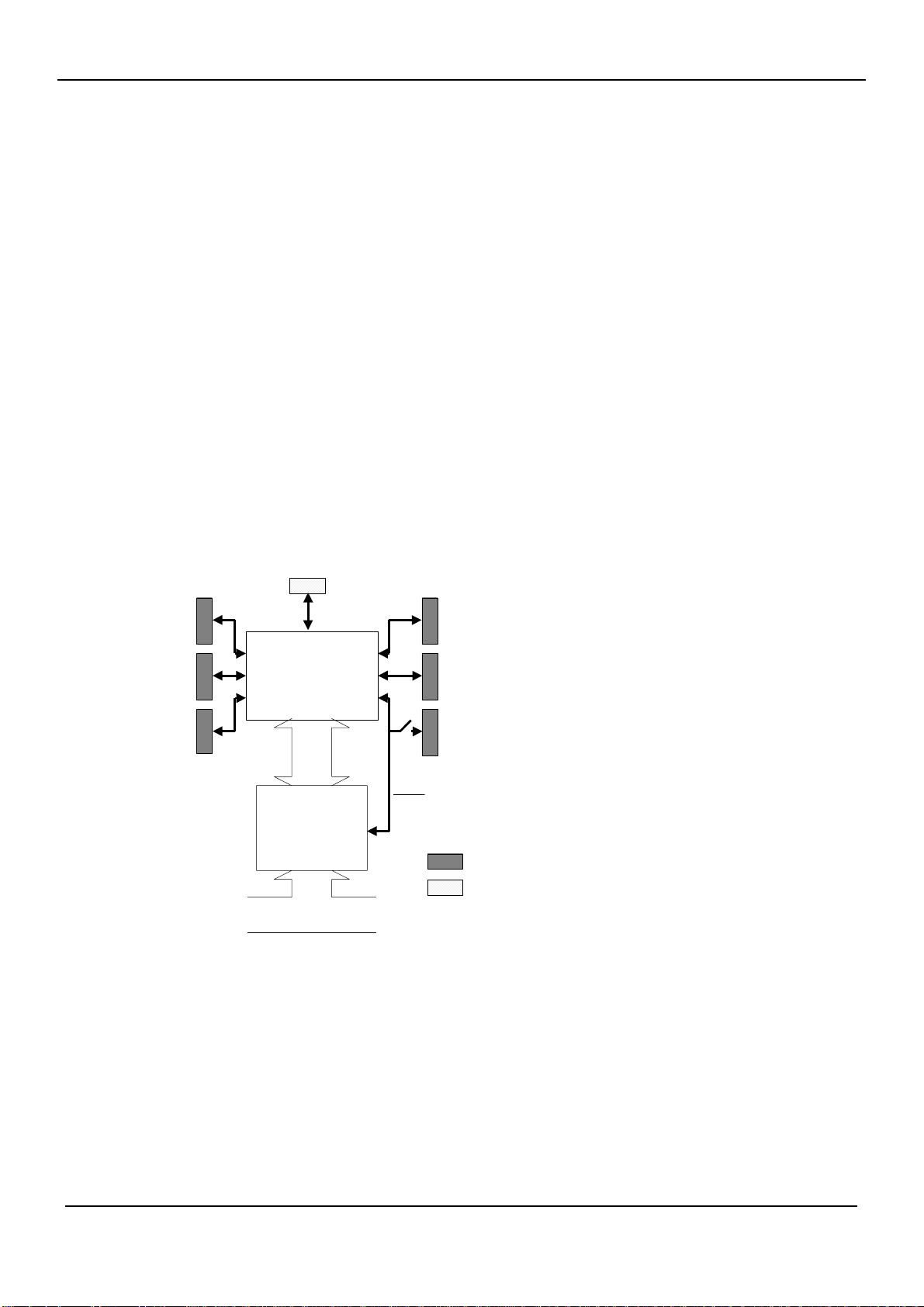
The SMT401 is a TIM carrier in the form of a PCI Mezzanine Card (PMC).
The board is equipped with a high bandwidth PCI interface, allowing it to be
hosted directly by any platform with a PCI bus (Revision 2.0 or later)
conforming to the IEEE P1386 (Common Mezzanine Card) standard.
1.1 Specifications:
• Accepts standard size 1 C40/C44 TIM
• 32-bit 33MHz PCI interface including:
• Bus master global bus to PCI interface with 43 MB/s
sustained throughput
• Host comm-port interface with >10Mbytes/s performance
• Up to six unbuffered Sundance comm-ports
• External JTAG access with master and slave ports
• 3.3V available to TIM
C2
C4x TIMC1
C4
Global
Bus
PCI
Interface
PCI BUS
Figure 1-1: Block Diagram of the SMT401
C5
C0
C3
Host comport
interface
Sundance comport
JTAG Front Panel IO
Document Name: SMT401 User Guide V1.2.doc Issue : 02 Rev.: 1.11
Product Name: SMT401 Revision Date: 07 December 2004
Author: Mark I. Cartlidge (Updated by SM, added JTAG slave section) Original Date: 12 May 1999
Page 4

Released Page 4 of 21 SMT401 PMC TIM Carrier User Guide
2 Installation
This chapter explains how to attach the SMT401 to a PMC motherboard.
2.1 Handling Instructions
• Observe the usual precautions for preventing damage to components by
electrostatic discharge. Personnel handling the board should be earthed.
• Avoid flexing the board along its length.
2.2 Setting Up 3.3V Supply
The SMT401 can supply 3.3V to a TIM site using the two plated mounting holes
next to the TIM sockets. The 3.3V can be supplied from the 3.3V pins on the PMC
connector or from an on board regulator. This selection is made via JP2 as follows
Link 3.3V supply
JP2 pin1 – JP2 pin2 3.3V from regulator
JP2 pin2 – JP2 pin3 3.3V from PMC connector
2.3 Installing a TIM onto the SMT401
Note: This operation should not be performed while the SMT401 is
powered up.
To install a TIM onto an SMT401, carry out the following procedure:
1. Place the TIM over the TIM sockets of the SMT401. Ensure
that the TIM is oriented correctly, as otherwise it will not fit
into the TIM sockets.
2. Apply sufficient but not excessive force to the TIM to push it
firmly into the TIM sockets.
3. Secure the TIM with M2.5 nylon bolts and nuts, using the two
holes next to the TIM connectors provided for this purpose. If
the TIM requires 3.3V (Sundance C6x TIM modules) the
supplied metal stand-offs and bolts should be used in place
of the nylon nuts and bolts. The 3.3V is supplied via the
plated mounting holes so it is essential that a good
connection is made between the plated mounting hole and
stand-off if the 3.3V supply is being used.
2.4 Installing the SMT401 onto a PMC carrier
Note: This operation should not be performed while the PMC carrier is
powered up.
The SMT401 must be affixed to the PMC carrier in the way shown below,
using the metal stand-offs, metal bolts and plastic washers provided:
Document Name: SMT401 User Guide V1.2.doc Issue : 02 Rev.: 1.11
Product Name: SMT401 Revision Date: 07 December 2004
Author: Mark I. Cartlidge (Updated by SM, added JTAG slave section) Original Date: 12 May 1999
Page 5

Released Page 5 of 21 SMT401 PMC TIM Carrier User Guide
SMT 401
PMC Motherboard
Figure 2-1: Attaching the SMT401 to a PMC Motherboard
Document Name: SMT401 User Guide V1.2.doc Issue : 02 Rev.: 1.11
Product Name: SMT401 Revision Date: 07 December 2004
Author: Mark I. Cartlidge (Updated by SM, added JTAG slave section) Original Date: 12 May 1999
Page 6
Released Page 6 of 21 SMT401 PMC TIM Carrier User Guide
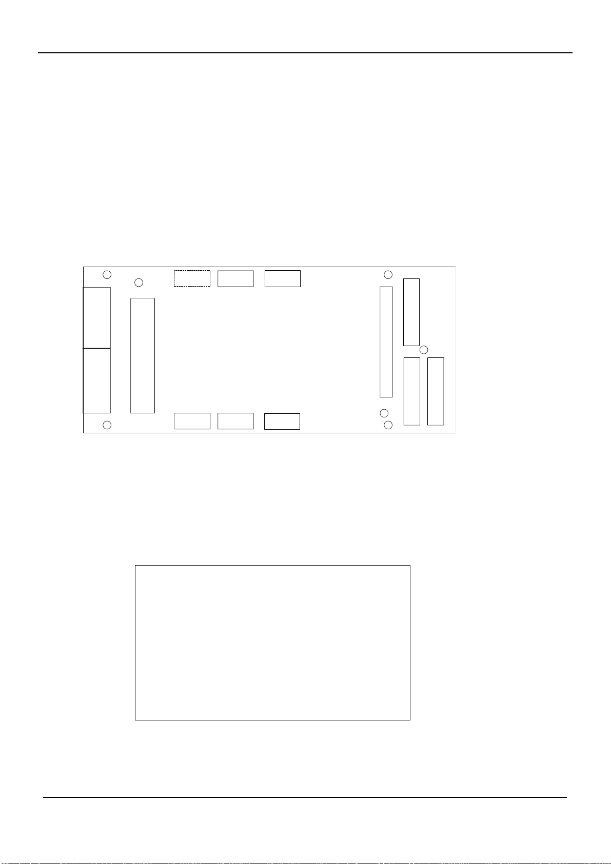
3 Connectors
This chapter details the connectors on the SMT401.
3.1 Comm-ports
The SMT401 has connections for up to six comm-ports, but usually only
there will only be five comm-ports available to the user, since one comm-port
is dedicated to the host comm-port interface (see figure 1.1, page 7).
Figure 3.1 shows the locations of the various connectors, and which C4x
comm-port they correspond to. C
by the C40 TIM:
denotes the comm-port number as seen
n
C
J10
0
C
5
JTAG OUT
Port
J2
C
3
J11 J15
(PMC connectors on this side)
JTAG IN
Port
J11 is used as the Host Comm port and is not normally available for connection
Figure 3-1: Comm-port Locations on SMT401
J1
J12J13
C
4
C
1
J14
C
2
As with all C4x comm-ports, it is important to observe the rule governing the
connection of RTO and RTI comm-ports:
Important Note
J10, J12, are RTO comm-ports
J11, J13 are RTI comm-ports
Do not connect a RTO comm-port to another
RTO comport
Do not connect a RTI comm-port to another RTI
comport
Failure to observe these rules can result in
permanent damage.
Document Name: SMT401 User Guide V1.2.doc Issue : 02 Rev.: 1.11
Product Name: SMT401 Revision Date: 07 December 2004
Author: Mark I. Cartlidge (Updated by SM, added JTAG slave section) Original Date: 12 May 1999
Page 7

Released Page 7 of 21 SMT401 PMC TIM Carrier User Guide
3.1.1 Sundance Comm-ports (J10, J11, J12, J13, J14, J15)
Sundance compatible comm-ports can be used to make connections over
short distances (30cm or less) to other Sundance comm-ports. The cables
should be fitted such that at one end, the blue insulation is face up, and
at the other, the blue insulation is face down.
3.2 JTAG Input & Output Ports
Both input and output ports for JTAG are be provided, these are compatible
with the SMT327 Compact PCI, SMT328 VME and other Sundance TIM
carriers.
The JTAG interface is designed to operate at up to 10MHz across up to 4
SMT401 motherboards.
There is no re-timing at the TDO output of each board in order to provide a
seamless chain of processors. This may limit the upper operating frequency
of the JTAG controller. By default this frequency will be 8.33MHz
(PCI_CLK/4) or less, depending on the PCI_CLK on the host.
Pin Signal Direction Description
1 TDI IN JTAG data in
2 GND
3 TDO OUT JTAG data out
4 GND
5 TMS IN JTAG Test mode select
6 GND
7 TCK IN JTAG clock, up to 10MHz
8 GND
9 TCK_RET OUT JTAG clock return
10 GND
11 -TRST IN JTAG Reset
12 GND
13 -RESET IN Board Reset in
14 PD OUT Presence detect, +5V 1A fused
15 -DETECT IN Detect external JTAG controller when grounded
16 CONFIG OPEN COLL Global open collector C4x CONFIG
17 EMU0 OUT Buffered EMU0 output
18 EMU1 OUT Buffered EMU1 output
19 SPARE1
20 SPARE2
Table 1 JTAG Slave Port (Input)
Document Name: SMT401 User Guide V1.2.doc Issue : 02 Rev.: 1.11
Product Name: SMT401 Revision Date: 07 December 2004
Author: Mark I. Cartlidge (Updated by SM, added JTAG slave section) Original Date: 12 May 1999
Page 8

Released Page 8 of 21 SMT401 PMC TIM Carrier User Guide
The SMT401 is used as a slave in a JTAG chain.
The SMT6012 user manual describes a typical master/slave configuration in
the chapter 6.
(http://www.sundance.com/docs/6012%20User%20Manual.pdf)
A JTAG Master such as a Sundance’s carrier board SMT310Q or SMT310
controls the SMT401 JTAG chain.
Any DSP module fitted on the SMT401 will appear in the DSP list of the
master chain.
For instance, a SMT376 is mounted into the SMT401, and the SMT310Q is
master of the SMT401.
The SMT310Q is connected to the SMT401 JTAGIN connector using a
Sundance Buffered JTAG cable (SMT501):
Figure 4-1: SMT401 JTAGIN as Slave JTAG connected to a SMT310Q as master JTAG
Document Name: SMT401 User Guide V1.2.doc Issue : 02 Rev.: 1.11
Product Name: SMT401 Revision Date: 07 December 2004
Author: Mark I. Cartlidge (Updated by SM, added JTAG slave section) Original Date: 12 May 1999
Page 9

Released Page 9 of 21 SMT401 PMC TIM Carrier User Guide
The setting-up of Texas Instruments Code Composer Studio must be done
MANUALLY, and is shown on the screenshot below:
Figure 5-1: TI CCS setup (SMT401 as Slave JTAG)
Document Name: SMT401 User Guide V1.2.doc Issue : 02 Rev.: 1.11
Product Name: SMT401 Revision Date: 07 December 2004
Author: Mark I. Cartlidge (Updated by SM, added JTAG slave section) Original Date: 12 May 1999
Page 10

Released Page 10 of 21 SMT401 PMC TIM Carrier User Guide
Pin Signal Direction Description
1 TDI OUT JTAG data out
2 GND
3 TDO IN JTAG data in
4 GND
5 TMS OUT JTAG Test mode select
6 GND
7 TCK OUT JTAG clock 10MHz
8 GND
9 TCK_RET IN JTAG clock return
10 GND
11 -TRST OUT JTAG Reset
12 GND
13 -RESET OUT Board Reset out
14 PD IN Presence detect when pulled high
15 -DETECT OUT Detect external JTAG controller when grounded
16 CONFIG OPEN COLL Global open collector C4x CONFIG
17 EMU0 IN Buffered EMU0 output
18 EMU1 IN Buffered EMU1 output
19 SPARE1
20 SPARE2
Table 2 JTAG Master Port (Output)
3.3 Control Header
An eight pin header, JP3, provides reset, the #CONFIG signal, and a jumper
which dictates when used under Parallel C whether the ADM-C4X is to act as
a link engine, or as an attached processor:
GND 1 2 #CONFIG
GND 3 4 #RESET_IN
GND 5 6 #BUSRESET
MODE (see below) 7 8 MODE (see below)
3.3.1 #CONFIG (JP3pins 1 & 2)
#CONFIG is an active-low, open-drain output from the SMT401. If there is a
TIM fitted to the SMT401 #CONFIG can be driven low, but never driven high,
by the TIM.
Pin 1 is provided simply as an associated ground signal for #CONFIG.
Document Name: SMT401 User Guide V1.2.doc Issue : 02 Rev.: 1.11
Product Name: SMT401 Revision Date: 07 December 2004
Author: Mark I. Cartlidge (Updated by SM, added JTAG slave section) Original Date: 12 May 1999
Page 11

Released Page 11 of 21 SMT401 PMC TIM Carrier User Guide
3.3.2 #RESET_IN (JP3 pins 3 & 4)
The #RESET_IN signal is used to reset the SMT401 TIM site when there is a
network of C4x processors upstream of the SMT401. Pin 3 can be used as a
ground signal for #RESET_IN.
For details on how to control #RESET_IN when the SMT401 is not used in
the Parallel C/AXP environment, refer to the document "SMT401
Programming Information" described in chapter 4.
3.3.3 #BUSRESET (JP3 pins 5 & 6)
The #BUSRESET signal is used to reset a network of C4x processors
downstream of the SMT401. Pin 5 can be used as a ground signal for
#BUSRESET.
For details on how to control #BUSRESET when the SMT401 is not used in
the Parallel C/AXP environment, refer to the document "SMT401
Programming Information" described in chapter 4.
3.3.4 MODE (JP3 pins 1 & 2)
When using the SMT401 under Parallel C/AXP, to configure the SMT401 as
an attached processor, connect pins 7 and 8 together with a shorting link. If
pins 7 and 8 are unconnected, the SMT401 acts as a link engine.
When not using Parallel C/AXP, a read-only flag, MODE, in the SMT401
Status register reflects whether or not pins 7 and 8 are connected together.
Refer to the document "SMT401 Programming Information" described in
chapter 4 for further information.
Document Name: SMT401 User Guide V1.2.doc Issue : 02 Rev.: 1.11
Product Name: SMT401 Revision Date: 07 December 2004
Author: Mark I. Cartlidge (Updated by SM, added JTAG slave section) Original Date: 12 May 1999
Page 12

Released Page 12 of 21 SMT401 PMC TIM Carrier User Guide
4 SMT401 Programming Registers
4.1 PCI Target Operation
In target mode, the SMT401 PMC is accessed by a host device across the
PCI bus. This allows access to the target mode registers. The operating
system or BIOS will normally allocate a base address for the target mode
registers of each SMT401 PMC. Access to each register within the SMT401
PMC is then specified by this base address and the offset shown in the table
below.
Offset Register(Write) Register(Read) Width
0 - -
+4 - -
+8 - -
+0C - -
+10 COMPORT OUT COMPORT IN 32
+14 CONTROL STATUS 32
+18 INT CONTROL - 32
+1C - LAST PCI ADD 32
+20 to +3F Not used Not used
+40 to +7E Reserved Reserved 32
4.2 Comm-port Registers (Offset 10h)
The host is connected to the first TIM site using comm-port 3. This port is
bidirectional and will automatically switch direction to meet a request from
either the host or the C40. Both input and output registers are 32 bits wide.
Data should only be written to COMPORT_OUT when STATUS[OBF] is 0.
Data received from the C40 is stored in COMPORT_IN and STATUS[IBF] is
set to 1. Reading COMPORT_IN will clear STATUS[IBF] and allow another
word to be received from the C40.
4.2.1 Control Register (Offset 14h)
The CONTROL register can only be written. It contains flags which control
the boot modes of the first TIM site.
Boot Control
Bit 7-5 4 3 2 1 0
Name Not used notNMI IIOF2 IIOF1 IIOF0 RESET
RESET Write a 1 to this bit to assert the reset signal to all TIM modules on the SMT401
PMC.
IIOF0 IIOF1, IIOF2 These bits connect to the corresponding pins on the first TIM site. These bits are
open-drain and can only pull down. If not required before or after booting they should
be written with 1’s.
NotNMI A 0 written to this bit will assert the active low NMI to the TIM1 C40.
Note. On PCI system reset, RESET is asserted to all TIM sites.
Document Name: SMT401 User Guide V1.2.doc Issue : 02 Rev.: 1.11
Product Name: SMT401 Revision Date: 07 December 2004
Author: Mark I. Cartlidge (Updated by SM, added JTAG slave section) Original Date: 12 May 1999
Page 13

Released Page 13 of 21 SMT401 PMC TIM Carrier User Guide
4.2.2 Status Register (Offset 14h)
The STATUS register can only be read.
Bit 31 30 29 28 27 26 25 24
Name MODE 0 0 0 0 IIOF2 IIOF1 IIOF0
Bit 23 22 21 20 19 18 17 16
Name 0 0 CONFIG_L TBC RDY 0 MASTER IBF OBF
Bit 15 14 13 12 11 10 9 8
Name 0 0 0 0 0 0 0 INTA
Bit 7 6 5 4 3 2 1 0
Name C40 INT TBC INT IBF INT OBE INT C40 IE TBC IE IBF IE OBE IE
OBE IE Set if comm-port output buffer empty interrupts enabled.
IBF IE Set if comm-port input buffer full interrupts enabled
TBC IE Set if JTAG interrupts enabled
C40 IE Set if interrupt from TIM1 C40 enabled
OBE INT Set if comm-port output buffer becomes empty.
Cleared by writing a 1 to the corresponding bit in the interrupt control register.
IBF INT Set if comm-port input buffer receives a word.
Cleared by writing a 1 to the corresponding bit in the interrupt control register
TBC INT Set when the TBC asserts its interrupt.
Cleared by removing the source of the interrupt in the TBC.
C40 INT Set when the TIM1 C40 sets its host interrupt bit.
Cleared by writing a 1 to the corresponding bit in the interrupt control register.
INTA This is a logical OR of bits 7 to 4 in this register gated with the corresponding enable bit.
OBF Set when a word is loaded into the comm-port output register. Cleared when the word is transmitted
to the C40.
IBF Set when a word is received into the comm-port input register from the TIM1 C40.
MASTER When set, the comm-port interface token is owned by the SMT401 PMC bridge.
TBC RDY Reflects the current state of the TBC RDY pin. This bit is active high and therefore an inversion of
the TBC pin.
CONFIG_L Reflects the current state of the CONFIG signal from the TIM1 C40. Active low.
IIOF0,1,2 These reflect the state of the IIOF pins
MODE Reserved for Alphadata use.
4.2.3 Interrupt Control Register (Offset 18h)
This write-only register controls the generation of interrupts on the PCI bus.
Each interrupt source has an associated enable and clear flag. This register
can be written with the contents of bits 7:0 of the Status Register.
Document Name: SMT401 User Guide V1.2.doc Issue : 02 Rev.: 1.11
Product Name: SMT401 Revision Date: 07 December 2004
Author: Mark I. Cartlidge (Updated by SM, added JTAG slave section) Original Date: 12 May 1999
Page 14

Released Page 14 of 21 SMT401 PMC TIM Carrier User Guide
Enable Group
Bit 7 6 5 4 3 2 1 0
Name CLEAR
C40 INT
0 CLEAR
IBF INT
CLEAROB
E INT
C40 IE TBC IE IBF IE OBE IE
IBF IE Input Buffer Full Interrupt Enable. Allows an interrupt to be generated when the host comm-port input
register is loaded with data from the C40.
OBE IE Output Buffer Empty Interrupt. Allows an interrupt to be generated when the host comm-port register has
transmitted its contents.
TBC IE Test Bus Controller Interrupt Enable. Interrupts from the Texas JTAG controller are enabled when set.
C40 IE C40 Interrupt Enable. Allows a programmed interrupt to be generated by the C40 when set.
CLEAR OBE
Write a one to this bit to clear the interrupt resulting from a comm-port output event.
INT
CLEAR IBF
Write a one to this bit to clear the interrupt event resulting from comm-port input.
INT
CLEAR C40
Write a one to this bit to clear down the C40 INT event.
INT
The JTAG controller which generates TBC INT must be cleared of all
interrupt sources in order to clear the interrupt.
4.3 PCI Master Operation
The first TIM position on the SMT401 PMC makes use of the global bus to
allow the C40 to read and write the entire PCI address space. Burst mode
and single transfers can be used to access the PCI address space.
Document Name: SMT401 User Guide V1.2.doc Issue : 02 Rev.: 1.11
Product Name: SMT401 Revision Date: 07 December 2004
Author: Mark I. Cartlidge (Updated by SM, added JTAG slave section) Original Date: 12 May 1999
Page 15

Released Page 15 of 21 SMT401 PMC TIM Carrier User Guide
)
)
PCI
ADI
O
Data
Add
C40
Decoder
32 bit
Add
Ctr
FIFO
16
x
32
FIFO
16
x
32
The C40 can access any PCI location but in should be noted that data written
and read will always be long word aligned and 32 bits wide. The table below
illustrates the available registers.
Address Register(Write
C0000000 FIFO FIFO 32
C0400000 PCI Address - 32
C0800000 Control - 2
Register(Read
Width
4.3.1 FIFO
The SMT401 PMC incorporates 16 deep x 32 wide FIFO buffers on both read
and write paths between the C40 and PCI bus. The FIFO is only effective
when burst mode is enabled in the control register. With burst mode disabled,
the bridge will request the PCI bus for each word transferred.
With burst mode enabled, data written to the empty FIFO will be absorbed
until 16 words make the FIFO full. This state will trigger a PCI burst write of
16 words in length thus transferring 64 bytes to the destination. The FIFO
can be written with the next 16 words during the PCI burst transaction to
maintain throughput. The C40 may incur wait states if the FIFO becomes full
during this time.
For burst mode read transactions, reading from the empty FIFO will trigger a
PCI burst of 16 words from source memory, filling the FIFO with 64 bytes of
data. The C40 will be able to read the first word of data as soon as it is
loaded into the FIFO from the PCI bus.
Transfers to / from the PCI space may not always be a multiple of 16 words.
In this case, the burst mode bit must be turned off to perform single transfers
for each word. For example, a transfer of 100 words could be performed as
follows :-
Document Name: SMT401 User Guide V1.2.doc Issue : 02 Rev.: 1.11
Product Name: SMT401 Revision Date: 07 December 2004
Author: Mark I. Cartlidge (Updated by SM, added JTAG slave section) Original Date: 12 May 1999
Page 16

Released Page 16 of 21 SMT401 PMC TIM Carrier User Guide
*add = pciAddress;
*control = BURST_ON;
for( i=0; i<96; i++ )
*fifo = data[i];
*control = BURST_OFF;
for( i=96; i<100; i++ )
*fifo = data[i];
The above code is not designed for speed but will cause burst action on the
PCI bus. DMA could replace the fifo loading to improve performance. The
PCI bridge will synchronise the burst enable bit in the control register to the
PCI burst cycle to maintain burst mode for each fifo payload of 16 words. The
address counter will not accept a new value whilst a PCI burst is in progress
or if either fifo is not empty.
Reading data from the PCI bus is the reverse of the above process. It should
be noted that with burst mode enabled, a read from the empty fifo will always
load 16 words from the PCI source.
4.3.2 PCI Address
The PCI address register is a 30 bit counter loaded from bits D31:2 of the
C40 data bus. The counter output is a 32 bit address with bits 1:0 always at
logic 0.
The PCI Address register must be written with a valid PCI address prior to
writing or reading from the FIFO. The value written into the address register
loses the bottom two bits in order to match the PCI bus mode used by the
bridge. The address counter increments on every valid PCI to track the
source or destination pointer in the event of a target disconnect. The bridge
may disconnect during burst transfers but this will be transparent to the C40.
4.3.3 C40 Control Register
The Control register provides the C40 interface with control over the
generation of interrupts on the PCI bus. Writing a 1 to the PCI INT bit will
generate an interrupt on the PCI bus via the INTA line. The interrupt is
cleared / acknowledged through the target interrupt control register.
Bit(s) 31-24 23:16 15:2 1 0
Name 0 0 0 PCI INT BURST
Document Name: SMT401 User Guide V1.2.doc Issue : 02 Rev.: 1.11
Product Name: SMT401 Revision Date: 07 December 2004
Author: Mark I. Cartlidge (Updated by SM, added JTAG slave section) Original Date: 12 May 1999
Page 17

Released Page 17 of 21 SMT401 PMC TIM Carrier User Guide
5 Sample Application
This chapter presents a sample application, to be run on one Alpha and an
attached C40, which performs case reversal on its text input. Although trivial,
it illustrates the main features of a mixed network application using the
SMT401 in attached processor mode. This section does not, explain how to
perform PCI transfers via the global bus; refer to the document "SMT401
Programming Information" described in chapter 5 of this manual.
The application is split into two tasks. The first, running on the Alpha, is the
front-end. The other runs on the attached C40 processor, and performs the
actual case reversal. The application can be represented thus:
driver
0
task
0
Alpha
0
caserev
task
0
C40
Figure 1: The Case Reversal Application
5.1 Configuration File
The configuration file describes the (minimum) physical network required by
the application and the logical connections between tasks, along with
information such as the memory requirements of each task.
PROCESSOR root TYPE=axp LINKS=5
PROCESSOR node TYPE=c40 LINKS=6 KERNEL="tim40.krn"
! The comm-port interface on SMT401
WIRE ? root[4] node[3]
TASK driver INS=1 OUTS=1 DATA=10K
TASK caserev INS=1 OUTS=1 DATA=10K
PLACE driver root
PLACE caserev node
CONNECT driver[0] caserev[0]
CONNECT caserev[0] driver[0]
Document Name: SMT401 User Guide V1.2.doc Issue : 02 Rev.: 1.11
Product Name: SMT401 Revision Date: 07 December 2004
Author: Mark I. Cartlidge (Updated by SM, added JTAG slave section) Original Date: 12 May 1999
Page 18

Released Page 18 of 21 SMT401 PMC TIM Carrier User Guide
5.2 Driver Task
The purpose of the driver task is to act as a front end to the case reversal
task:
#include <stdio.h>
#include <chan.h>
main(int argc, char* argv[], char* envp[],
CHAN* in_ports[], int ins,
CHAN* out_ports[], int outs)
{
int c;
for (;;) {
c = getchar();
chan_out_word(c, out_ports[0]);
if (c == EOF)
break;
chan_in_word(&c, in_ports[0]);
putchar(c);
}
exit(0);
}
5.3 Case Reversal Task
The case reversal task receives characters from the driver task, inverts their
case if alphabetic, and then returns them to the driver task.
#include <stdio.h>
#include <ctype.h>
#include <chan.h>
main(int argc, char* argv[], char* envp[],
CHAN* in_ports[], int ins, CHAN* out_ports[], int
outs)
{
int c;
Document Name: SMT401 User Guide V1.2.doc Issue : 02 Rev.: 1.11
Product Name: SMT401 Revision Date: 07 December 2004
Author: Mark I. Cartlidge (Updated by SM, added JTAG slave section) Original Date: 12 May 1999
Page 19

Released Page 19 of 21 SMT401 PMC TIM Carrier User Guide
for (;;) {
chan_in_word(&c, in_ports[0]);
if (c == EOF)
break;
if (islower(c))
c = toupper(c);
else if (isupper(c))
c = tolower(c);
chan_out_word(c, out_ports[0]);
}
}
Document Name: SMT401 User Guide V1.2.doc Issue : 02 Rev.: 1.11
Product Name: SMT401 Revision Date: 07 December 2004
Author: Mark I. Cartlidge (Updated by SM, added JTAG slave section) Original Date: 12 May 1999
Page 20

Released Page 20 of 21 SMT401 PMC TIM Carrier User Guide
6 Copyright
Copyright © Sundance Multiprocessor Technology Ltd. 1999, 1997 Alpha
Data Parallel Systems Ltd. All rights reserved.
This publication is protected by Copyright Law, with all rights reserved. No
part of this publication may be reproduced, in any shape or form, without
prior written consent from Sundance Multiprocessor Technology Ltd.
7 About this Manual
7.1.1 Important Note
Before unpacking and using any the product detailed in this manual, please
read the handling instructions described in section 2.1.
Improper handling of units could result in permanent damage to them.
7.1.2 Purpose of this manual
This manual describes how to install and configure the SMT401 PMC TIM
Motherboard.
7.1.3 Reserved rights
This manual is designed to provide outline information only. Sundance has a
continual policy of improving its products; hence it reserves the right to
change product specification without prior warning. Sundance cannot accept
any liability for loss or damages arising from the use of this manual or the use
of products detailed within it.
7.1.4 Trademark acknowledgements
The following are trademarks of Digital Equipment Corporation:
Alpha AXP, PDP-11, VAX, VMS and ULTRIX.
OSF/1 is a registered trademark of the Open Software Foundation, Inc.
UNIX is a registered trademark of UNIX System Laboratories, Inc.
IBM is a registered trademark, and PC/AT is a trademark of International
Business Machines Corporation.
MS-DOS is a registered trademark of Microsoft Corporation.
Intel is a registered trademark of Intel Corporation.
3L is a registered trademark of 3L Ltd.
7.1.5 Warranty and Support
All Sundance products enjoy parts and labour warranty for 12 months after
purchase. The warranty is based on the customer returning the defective
goods to Sundance for repair or replacement, which will be at the discretion
of the company. The warranty does not cover damages caused by
Document Name: SMT401 User Guide V1.2.doc Issue : 02 Rev.: 1.11
Product Name: SMT401 Revision Date: 07 December 2004
Author: Mark I. Cartlidge (Updated by SM, added JTAG slave section) Original Date: 12 May 1999
Page 21

Released Page 21 of 21 SMT401 PMC TIM Carrier User Guide
negligence, misuse, and normal wear and tear. No liability is accepted by the
company for any damage caused by the use of its hardware or software.
All goods from Sundance carry a 6 months free support service. This service
is available by letter, phone, fax, and email. Technical support contracts for
longer periods are available on request. Support contracts for software
components also normally cover the cost of upgrades.
Document Name: SMT401 User Guide V1.2.doc Issue : 02 Rev.: 1.11
Product Name: SMT401 Revision Date: 07 December 2004
Author: Mark I. Cartlidge (Updated by SM, added JTAG slave section) Original Date: 12 May 1999
 Loading...