

Page 1

USER GUIDE
FOR
SMT398VP
Copyright © Sundance
All rights reserved. No part of this document may be reproduced, translated,
stored in a retrieval system, or transmitted, in any form or by any means,
electronic, mechanical, photocopying, recording or otherwise, without prior
written permission of the owner.
If this copy is no longer in use, return to sender.
SMT398VP-D000058H-guide.doc
Document No.
Note:
Revision
2.4.2
Date
Page 1 of 34
08/02/07
Page 2
APPROVAL PAGE
Name Signature Date
AUTHOR/S
Name Signature Date
E. Puillet 29/01/2005
G. Parker 9/12/2005
SMT398VP-D000058H-guide.doc
Document No.
Revision
2.4.2
Date
Page 2 of 34
08/02/07
Page 3
DOCUMENT HISTORY
Date Initials Revision Description of change
06/05/06 E.P 2.0 New document
12/07/06 E.P 2.0.1 Update of figure 5
28/07/06 E.P 2.0.2 Update of figure 3
02/08/06 E.P 2.1 Addition of SMT398VP Reset scheme.
21/08/06 E.P 2.2 Addition of JTAG Header pinout.
25/08/06 E.P 2.3 Update of RSLs’ pinout.
18/09/06 E.P 2.4 Clarifications on clock synthesizer crystal frequency.
Update of board Top view with T1.
19/09/06 E.P 2.4.1 Correction of the amount of Leds available.
Addition of TIM connector reference in chapter Pinout.
08/02/07 E.P 2.4.2 Clarification of Switch name and positions.
SMT398VP-D000058H-guide.doc
Document No.
Revision
2.4.2
Date
Page 3 of 34
08/02/07
Page 4

TABLE OF CONTENTS
1. SCOPE.................................................................................................................................................................................7
1.1. INTRODUCTION ............................................................................................................................................................7
1.2. PURPOSE ......................................................................................................................................................................7
1.3. APPLICABILITY ............................................................................................................................................................7
2. APPLICABLE DOCUMENTS AND REFERENCES....................................................................................................8
2.1. APPLICABLE DOCUMENTS............................................................................................................................................8
2.1.1. External Documents ...............................................................................................................................................8
2.1.2. Internal documents.................................................................................................................................................8
2.1.3. Project Documents .................................................................................................................................................8
2.2. REFERENCES ................................................................................................................................................................8
2.2.1. External documents................................................................................................................................................8
2.2.2. Internal documents.................................................................................................................................................8
2.2.3. Project documents..................................................................................................................................................8
2.3. PRECEDENCE................................................................................................................................................................8
3. ACRONYMS, ABBREVIATIONS AND DEFINITIONS ............................................................................................10
3.1. ACRONYMS AND ABBREVIATIONS..............................................................................................................................10
3.2. DEFINITIONS ..............................................................................................................................................................10
4. FEATURES.......................................................................................................................................................................11
4.1. THE SMT398VP TIM ................................................................................................................................................11
4.1.1. SMT398VP Diagram............................................................................................................................................11
4.1.2. Interface Definition ..............................................................................................................................................12
4.1.3. Major features......................................................................................................................................................12
4.1.4. Prime Item Characteristics...................................................................................................................................12
4.1.5. Performance.........................................................................................................................................................20
4.1.6. Physical Characteristics.......................................................................................................................................21
5. FOOTPRINT ....................................................................................................................................................................23
5.1. TOP VIEW ..................................................................................................................................................................23
5.2. BOTTOM VIEW...........................................................................................................................................................24
6. PINOUT.............................................................................................................................................................................25
6.1. FPGA ........................................................................................................................................................................25
6.1.1. RSLs ......................................................................................................................................................................25
6.2. CONNECTORS.............................................................................................................................................................27
6.2.1. RSLs ......................................................................................................................................................................27
6.3. SHB...........................................................................................................................................................................29
6.4. SLB ...........................................................................................................................................................................29
6.5. JTAG.........................................................................................................................................................................29
6.6. TIM CONNECTORS.....................................................................................................................................................30
7. ORDERING INFORMATION........................................................................................................................................31
8. QUALIFICATION REQUIREMENTS .........................................................................................................................32
8.1. QUALIFICATION TESTS...............................................................................................................................................32
8.1.1. Meet Sundance standard specifications ...............................................................................................................32
8.1.2. Speed qualification tests.......................................................................................................................................33
8.1.3. Integration qualification tests...............................................................................................................................33
9. HARDWARE SUPPORT PACKAGE............................................................................................................................34
Document No.
Revision
Date
Page 4 of 34
SMT398VP-D000058H-guide.doc
2.4.2
08/02/07
Page 5

TABLE OF FIGURES
Figure 1: Block Diagram.............................................................................................................................11
Figure 2: CPLD state machine.....................................................................................................................14
Figure 3: FPGA connections to Bank1 of QDRII .......................................................................................15
Figure 4: Clocking distribution diagram .....................................................................................................19
Figure 5: Top View......................................................................................................................................23
Figure 6: Bottom View................................................................................................................................24
Figure 7: JTAG connector Top View..........................................................................................................29
SMT398VP-D000058H-guide.doc
Document No.
Revision
2.4.2
Date
Page 5 of 34
08/02/07
Page 6

TABLE OF TABLES
Table 1: Communication standard supported by Rocket IO transceivers...................................................17
Table 2: DIP switch for special reset feature...............................................................................................18
Table 3: DIP switch for the selection of the configuration bitstream source..............................................18
Table 4: Clock synthesizer Configurations for Rocket IO standard application.........................................20
Table 5: Power budget.................................................................................................................................21
Table 6: QDR II termination scheme...........................................................................................................22
Table 7:RSL reference clocks......................................................................................................................25
Table 8:RSL-TOP (J5) connector Type A...................................................................................................27
Table 9: RSL-BOTTOM (J6) connector Type B.........................................................................................27
Table 10:RSL-TOP (J3) connector Type B.................................................................................................28
Table 11: RSL-BOTTOM (J4) connector Type A ......................................................................................28
Table 12: JTAG connector pinout. ..............................................................................................................30
SMT398VP-D000058H-guide.doc
Document No.
Revision
2.4.2
Date
Page 6 of 34
08/02/07
Page 7

1. SCOPE
This document provides practical information on the resources available on the SMT398VP. It also
describes how to use the features of SMT398VP FPGA Tim module.
1.1. INTRODUCTION
The SMT398VP is an FPGA TIM module designed to be integrated in modular systems.
It is designed to connect to the huge range of other TIM modules and carriers developed by
Sundance.
Sundance modular solutions provide flexible and upgradeable systems.
The SMT398VP is a TIM module aimed at completing the range of Sundance Virtex II-Pro
FPGA modules like SMT351, SMT338-VP, SMT387 and SMT395.
It provides a communications platform between an XC2VP70 Virtex-II Pro FPGA and
• On-board Double Data Rate Dual Port QDR II memory at frequencies of up to
200MHz.
• Rocket IOs for high speed serial connections capable of various high-speed serial
standards.
• LVDS connections for high speed parallel connections
• LVTTL connections and connectors.
This variety of connectors and interfaces provides a wide range of development options for
designers to explore the capabilities of the comprehensive Sundance TIM modules and carriers
family.
1.2. PURPOSE
The SMT398VP provides:
• High-speed interface to Sundance ADC/DAC modules/mezzanines.
• High-speed interface to Sundance DSP modules.
• High-speed interface to a Host via Sundance RSL carriers. (SMT145)
• Provide high-speed serial or parallel interface to the outside world.
• Fit in any configuration on Sundance carriers, i.e on its own, on a stand-alone carrier or
in a Host as part of a system.
1.3. APPLICABILITY
Interface to other FPGA, DSP, ADC/DAC modules and in stand alone systems.
SMT398VP-D000058H-guide.doc
Document No.
Revision
2.4.2
Date
Page 7 of 34
08/02/07
Page 8

2. APPLICABLE DOCUMENTS AND REFERENCES
2.1. APPLICABLE DOCUMENTS
2.1.1. External Documents
TI TIM specification & user’s guide.
Samtec QSH Catalogue page
Samsung QDR II Datasheet
Virtex II Pro Datasheet
2.1.2. Internal documents
SUNDANCE SDB specification.
SUNDANCE SHB specification
SUNDANCE SLB specification
SUNDANCE RSL specification
SUNDANCE SMT6500
SUNDANCE SMT6400
Sundance Help file
Sundance D000110-spec.pdf clock synthesizer FPGA task design.
2.1.3. Project Documents
D000058H-proj.mpp Software Planning Document for SMT398VP.
2.2. REFERENCES
2.2.1. External documents
N.A
2.2.2. Internal documents
N.A
2.2.3. Project documents
N.A
2.3. PRECEDENCE
In the event of conflict between the text of this document, and the applicable documents cited
herein, the text of this document takes precedence. Nothing in this document however,
SMT398VP-D000058H-guide.doc
Document No.
Revision
2.4.2
Date
Page 8 of 34
08/02/07
Page 9

supersedes applicable laws and regulations unless a specific exemption has been obtained and
is identified in the text of this document.
SMT398VP-D000058H-guide.doc
Document No.
Revision
2.4.2
Date
Page 9 of 34
08/02/07
Page 10

3. ACRONYMS, ABBREVIATIONS AND DEFINITIONS
3.1. ACRONYMS AND ABBREVIATIONS
TIM Texas Instruments Module
TI© DSP Texas Instrument Digital Signal Processor
Xilinx©
Xilinx© Field Programmable Gate Array.
FPGA
QDR Quad Data Rate
CP ComPort. Communication interface
SDB Sundance Digital Bus. Communication interface
SHB Sundance High-Speed Bus. Communication interface
RSL Rocket io Serial Link. Communication interface
MGT Multi Gigabit Transceiver
3.2. DEFINITIONS
DSP Module Typically a TIM module hosting a TI DSP and, a Xilinx FPGA.
FPGA-only Module A TIM with no on-board DSP, where the FPGA provides all
functionality.
Firmware A proprietary FPGA design providing some sort of functionality.
Sundance Firmware is the firmware running in an FPGA of a DSP
module.
SMT398VP-D000058H-guide.doc
Document No.
Revision
2.4.2
Date
Page 10 of 34
08/02/07
Page 11
4. FEATURES
4.1. THE SMT398VP TIM
This module conforms to the TIM standard (Texas Instrument Module, See TI TIM
specification & user’s guide) for single width modules.
It sits on a carrier board.
The carrier board provides power, Ground, communication links (ComPort links, RSL links)
between all the modules fitted and a pathway to the host, for a non stand-alone system.
The SMT398VP requires an additional 3.3V power supply (as present on all Sundance TIM
carrier boards), which must be provided by the two diagonally opposite mounting holes.
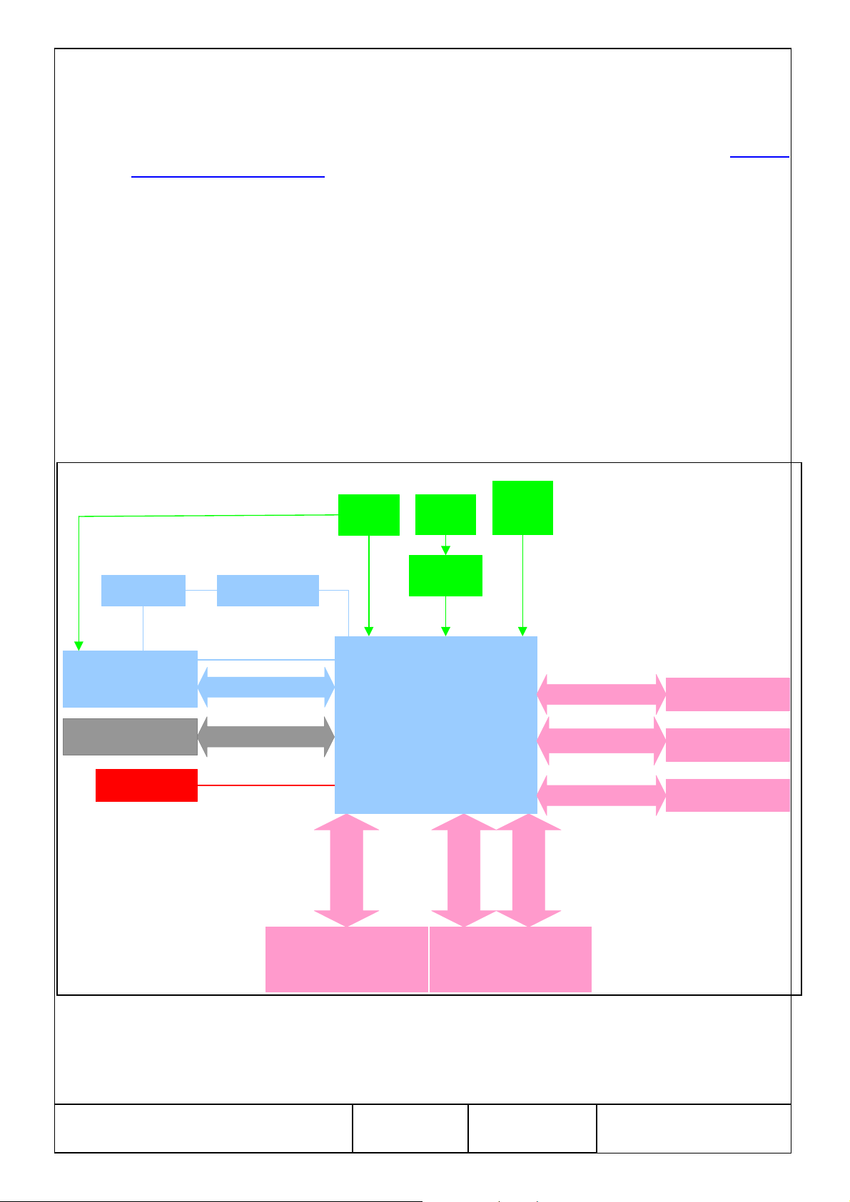
4.1.1. SMT398VP Diagram
Figure 1 shows a simplified version of the SMT398VP module.
JTAG Header
JTAG
Xilinx Coolrunner II
CPLD XC2C128VQ100
on Comport[0;3] and
Config&control
4 Mbytes QDR II-SRAM
2x (512kx36)
4 LEDs or
4 I/O pins
PROM
XCF32PVO48
JTAG
16 I/O pins
208 I/O pins; 36-bit data
50MHz
Oscillator
Virtex-II Pro FF1517
852 to 964 I/O Pins
48 I/O pins
4x Comm-Port/SDL
25MHz
Crystal
Clock
Synthesizer
FPGA
XC2VP70
1.5V Core
1.5V/3.3V I/O
External
clock
MMCX
(optional)
120 I/O pins
20 differential pairs
40 TTL IOs
16 RocketIO links
24 I/O pins
2x Comports/SDL
5 I/O pins
Interrupts&Reset
Sundance High
speed Bus (2 Conn.)
Sundance Low
voltage Bus (1 Conn.)
Sundance Rocket io
Serial Link (4 Conn.)
J2 Bottom Primary TIM
Connector
4xComport/SDL 1;2;4 & 5
Figure 1: Block Diagram
SMT398VP-D000058H-guide.doc
Document No.
Revision
2.4.2
J1 Top Primary TIM
Connector
Comport 0 & 3
Date
Page 11 of 34
08/02/07
Page 12

4.1.2. Interface Definition
For the TIM to carrier board or external world interfacing, see in Sundance Help file (that
you can download from this link)
4.1.3. Major features
• Block1: Xilinx Virtex II Pro XC2VP70, configuration scheme and reset scheme.
• Block2: QDR II SRAM memory.
• Block3: IO connectors for general purpose or dedicated interfaces.
• Block4: Clocking scheme performing from 25 MHz up to 700MHz.
• Block5: Leds for development and in-use monitoring and general purpose use.
4.1.4. Prime Item Characteristics
4.1.4.1. FPGA
Xilinx Virtex II Pro XC2VP70FF1517 FPGA.
This device is packaged in a 1517-pin BGA package with a -6 or -7 speed grade. It
contains 2 PowerPC 405s and up to 16 Rocket-I/Os.
4.1.4.2. CPLD
Xilinx Coolrunner II device XC2C128-6VQ100C This device is packaged in a 100pin very Thin QFP package with a -6 speed grade.
It provides the option to configure the FPGA via ComPort 0 or 3 at 20Mbytes/s.
Ideal for quick in systems debugging/prototyping and development of your FPGA
design where the SMT398VP is coupled to at least 1 DSP TIM. It also enables insystem updates.
The CPLD code is NOT to be modified without Sundance approval.
4.1.4.3. PROM
Xilinx Flash PROM device
XCF32PVO48.
Programmed via JTAG.
Loads an FPGA configuration bitstream at power up or reset.
Parallel FPGA configuration interface (up to 33 MHz)
Built-in data decompressor compatible with Xilinx advanced compression
technology.
SMT398VP-D000058H-guide.doc
Document No.
Revision
2.4.2
Date
Page 12 of 34
08/02/07
Page 13

4.1.4.4. JTAG Header
The JTAG header is compatible with Xilinx Parallel-IV cable signals.
It supports code download (for the FPGA Power PC), FPGA configuration,
Hardware and Software Debugging tools for the Virtex-II Pro.
This cable connects the parallel port of an engineer's Workstation/PC to the JTAG
chain of the SMT398VP Module.
All the devices from block1 are chained and accessible via this JTAG header.
4.1.4.5. FPGA Configuration schemes
Different schemes are available to provide maximum flexibility in systems where the
SMT398VP is involved:
The FPGA configuration bitstream source can be:
• one of the 2 ComPorts:
The CPLD is connected to 2 ComPort links of the SMT398VP TIM connector. A
switch (see Table 3) is used to select the configuration ComPort that will be used to
receive the bitstream.
The CPLD allows for FPGA configuration in slave SelectMap mode.
• On-board Flash PROM.
The FPGA configuration is operated in Master SelectMap mode. A switch (see Table
3) is used to select PROM as the configuration source.
• Using the on-board JTAG header and Xilinx JTAG programming tools.
The JTAG header is a
4.1.4.6. FPGA Reset Scheme
The CPLD is connected to a TIM global Reset signal provided to the SMT398VP via
its primary TIM connector pin 30. (See Figure 5: Top View)
Parallel-IV Header.
The CPLD provides another signal called FPGAResetn that offers a better Reset
control over the FPGA.
At power up or on reception of a low TIM global Reset pulse, the CPLD drives the
FPGAResetn signal low and keeps it low.
When the ENDKEY has been received, the CPLD drives FPGAResetn high.
Use FPGAResetn for the Global Reset signal of your FPGA designs.
In this manner, you can control your FPGA design Reset activity and you will also
avoid possible conflicts on ComPort 3 if your FPGA design implements it.
SMT398VP-D000058H-guide.doc
Document No.
Revision
2.4.2
Date
Page 13 of 34
08/02/07
Page 14

The Reset control is operated by the CPLD line FPGAResetn.
The following diagram shows the CPLD states after Reset.
Figure 2: CPLD state machine
SMT398VP-D000058H-guide.doc
Document No.
Revision
2.4.2
Date
Page 14 of 34
08/02/07
Page 15

4.1.4.7. QDR II SRAM
Up to 4 Mbytes of QDR II SRAM
The memory is available as 2 independent banks of QDRII. Each bank is arranged as
follows:
VTERM=VREF/2
QDRII
Bank x
Addr
D
Ctrl
Q/Qn
C/Cn
K/Kn
Q
R = 50 Ohms
XC2VP
QK/QKn, QC/QCn (output)
QQ[35:0]
QD[35:0]
NC + QSA[16:0]
QWn/QRn
CQ/CQn (input)
R = 50 Ohms
VTERM=VREF/2
Figure 3: FPGA connections to Bank1 of QDRII
4 word burst-QDR II at 200MHz in 2 independent banks of 36-bits wide data busses.
The aggregate throughput for data transfers with the QDR II is 28.8 Gb/s, or 400
Mb/s per pin for a 36-bit write bus and a 36-bit read bus operating in DDR mode at
200 MHz.
Each bank is fully independent with separate address, control and data busses.
The 2 devices used are Samsung K7R163684B-FC20. Alternative part numbers,
fully compatible can be fitted depending on availability at time of order.
36
36
36
20
20
2
2
2
36
4
Alternative part numbers are:
μPD44165364F5-E50-EQ1
Specification and implementation documents are available for design details about
using the QDRII .
SMT398VP-D000058H-guide.doc
Document No.
Revision
2.4.2
Cypress CY7C1315AV18-200BZC or NEC
Date
Page 15 of 34
08/02/07
Page 16

4.1.4.8. Sundance High speed Bus
2 x 60 pins connectors provide 120 io connections between the FPGA and the
outside word.
They allow interfacing to other Sundance modules providing that you implement an
SHB interface in the FPGA. (See 2.1.2. )
The SHB interface is available in Sundance SMT6500 support package.
They allow interfacing to the outside world by implementing your own interface in
the FPGA.
The FPGA io banks hosting the SHB signals are powered using Vcco = 3.3v.
4.1.4.9. Sundance Low voltage Bus
1 x 60 LVDS pairs io connections between the FPGA and the outside world.
They allow interfacing to Sundance mezzanine modules providing that you
implement an SLB interface in the FPGA. (See
interfaces to the mezzanines supported on this module.
2.1.2. ). Sundance provides the
For the mezzanines supported, please contact Sundance technical support, as more
mezzanines are supported over time.
They allow interfacing to the outside world by implementing your own LVDS
interface in the FPGA.
The FPGA io banks hosting the SLB signals are powered using Vcco = 2.5v.
4.1.4.10. Sundance Rocket io Serial Link
4 x 4 MGTs (part of the VII PRO FPGA silicon) io connections between the FPGA
and the outside world.
They allow interfacing to Sundance TIM modules or to a Host PC providing that you
implement a RSL Interface inside the FPGA
Each MGT has separate transmit and receive functions (full-duplex) and can be
operated at baud rates from 600 Mbits/s to 3.125 Gbits/s.
To accommodate for these various frequencies a clock synthesizer is available on the
module. (See 4.1.4.13. )
Additionally, every RocketIO MGT block is fully independent and contains a
complete set of common SerDes (serializer/deserializer) functions.
This allows Virtex-II Pro devices to support many existing and emerging serial I/O
standards at data rates up to 10 Gbits/s (when cumulating 4 channels)(see Xilinx for
supported standards).
SMT398VP-D000058H-guide.doc
Document No.
Revision
2.4.2
Date
Page 16 of 34
08/02/07
Page 17

• Up to 16 DC coupled Rocket I/Os are available.(Rocket I/Os can be AC coupled
on demand).
• The 16 MGTs can be configured to implement different MGT interfaces. A
mezzanine board which can plug on the SMT398VP RSL connector could
potentially provide the connectors needed by the serial IO standard, for instance:
Infiniband, Serial ATA, Ethernet channels...
• The maximum transfer rate is 2.5Gbits/s on a Virtex II Pro -6 part.
Mode Channels IO bit rate (Gb/s)
1.06 Fiber Channel 1
2.12
Gigabit Ethernet 1 1.25
XAUI (10 Gbit Ethernet) 4 3.125
Infiniband 1, 4, 12 2.5
Aurora 1, 2, 3, 4 0.600-3.125
Custom 1, 2, 3, 4 0.600-3.125
Table 1: Communication standard supported by Rocket IO transceivers
4.1.4.11. TIM Connectors
TIM connectors provide 6 communication links (ComPorts) to the FPGA.
They allow interfacing to Sundance TIM modules or to a Host PC providing that you
implement a ComPort Interface inside the FPGA. (See 2.1.2. )
The ComPort interface is available in Sundance SMT6500 support package.
The FPGA io banks hosting the ComPort signals are powered using Vcco = 3.3v.
The TIM connectors also provide power/ground, reset and various control signals.
References and specifications for these connectors are available on Sundance Web
site.
SMT398VP-D000058H-guide.doc
Document No.
Revision
2.4.2
Date
Page 17 of 34
08/02/07
Page 18

4.1.4.12. DIP Switches
• Two four-position DIP switches are connected to the CPLD to provide
control over the selection of the configuration bitstream source, and a special
reset feature called “TIM Confign”. (See Bottom View)
SW1 pos 4
TIM Confign
ON ENABLED
OFF DISABLED
Table 2: DIP switch for special reset feature
SW1 pos 3,2, 1
JPC3 JPC2 JPC1
C0P ON ON ON
C3P OFF OFF OFF
PROM OFF OFF ON
Table 3: DIP switch for the selection of the configuration bitstream source
4.1.4.13. Clocking scheme
The SMT398VP module provides a 50MHz LVTTL clock and a clock synthesiser.
• 50 MHz LVTTL oscillator: Main system clock. Clocks the CPLD and the
FPGA. Can be input in a DCM.
ICS clock synthesizer 8442, used to generate any frequencies between 31.25
•
MHz up to 700MHz with a jitter lower than 40ps required for the Rocket I/O
transceiver REFCLK input.
A 25MHz Crystal is used on this board as the input to the clock synthesizer’s
on-chip oscillator.
The TEST output from the clock synthesizer is not available on a pin of the
FPGA but can be observed from the board directly from hole T1 (See
5: Top View
)
Figure
The clock synthesiser is programmed by the FPGA.
The clock synthesiser’s differential LVDS outputs are both available on pins
of the FPGA as pre Figure 4: Clocking distribution diagram.
SMT398VP-D000058H-guide.doc
Document No.
Revision
2.4.2
Date
Page 18 of 34
08/02/07
Page 19

A Specification document D000110-spec.pdf about a design programming
the clock synthesiser is available from Sundance. The implementation
reference design is provided with the board package.
• An external clock input is provided to the Virtex II Pro FPGA via an MMCX
connector. This connector is NOT fitted by default or if a mezzanine is
required. YOU MUST ask Sundance if needed for your application.
User
CLK
MMCX
(optinal)
25MHz XTAL
CLK
Synthesis
AK20
QDRII
A
CQ
CQn
K
Kn
C
Cn
V38
R36
N37
P37
N31
M32
M21L21
D20 E20
6s7p
5p 4s
+ -
BANK 0 BANK 1
DCM
CLKFX
IN
CLKDIV
CLK2X
FB
[X0,X1]Y1
CLK0
TIM Conn CLKIN
ShbA
Hw0
S CLOCK
Clk
50Mhz
K20 M20N20J20
F15
3p
2s
FB
DCM
[X2,X3]Y1
CLKFX
CLK0
osc
1p
IN
CLKDIV
CLK2X
ShbA
Hw1
Clk
0s
BANK 2
CQ
QDRII
B
CQn
K
Kn
C
Cn
AM37
AG30
AE37
AD37
AD32
AC32
Figure 4: Clocking distribution diagram
FB
[X0,X1]Y0
BANK 6 BANK 7
CLK0
- +
7s 6p
AT20AR20
CLK
Synthesis
VIIPRO
IN
DCM
CLKFX
CLKDIV
CLK2X
[X2,X3]Y0
CLK0
BANK 5 BANK 4
AH21 AJ21 AH20
4p5s
3s
ShbB
Hw0
Clk
FB
DCM
CLKFX
2p
IN
CLKDIV
CLK2X
1s
AL20
ShbB
Hw1
Clk
BANK 3
0p
AK20AG20
Document No.
SMT398VP-D000058H-guide.doc
Revision
2.4.2
Date
Page 19 of 34
08/02/07
Page 20

Mode Frequency
ICS8442 output frequency to
SERDES (MHz)
(MHz)
53.125 1.06 Fiber Channel 25
106.25 2.12
Gigabit Ethernet 25 125
250
156.25
Infiniband 25 250 2.5
Aurora Custom Custom 0.600-3.125
Custom Custom Custom 0.600-3.125
Table 4: Clock synthesizer Configurations for Rocket IO standard application
IO bit rate
(Gb/s)
1.25
2.5
3.125
4.1.4.14. Leds
4.1.5. Performance
The FPGA features like speed grade and density dictate most performances.
The performances achievable by the other components are given in the
Characteristics
• 3 Red Leds connect to the FPGA and are available to the User: D2, D3, D4
• 1 Green Led: D5, connects to the DONE pin of the FPGA and is lit to show
that the FPGA is configured. (depending on supply from manufacturer a red
led can be fitted).
•
4.1.4. Prime Item
chapter.
SMT398VP-D000058H-guide.doc
Document No.
Revision
2.4.2
Date
Page 20 of 34
08/02/07
Page 21

4.1.6. Physical Characteristics
4.1.6.1. Power budget
Table 5: Power budget.
Device
Static Power on termination
resistor (50 ohms) (See
details)
Samsung QDR II burst 4
(36-bit interface)
25 Mhz Clock oscillator 1 3.3 10 0.033 Jauch VX3 Quartz crystal oscillators
Digital 3.3 155 0.5115 Clock
synthesizer
Analog
LEDs 5 3.3 25 0.4125
DIP Switch 1 2.5 2.1 0.005 Four 4.7 Kohm pullup
XC2V70 FPGA 1 Must be calculated based on design. Xpower
Coolrunner II CPLD (See
details)
Quantity Voltage(V) Current(mA) Power(W) Source
200 1.8 16.0 5.76
2 1.8 550 1.98 Samsung QDRII datasheet
1
3.3 20 0.066
tool from Xilinx should be used
1 1.8 17mA 0.031 CPLD power calculator
Virtex II PRO (ds083 module 3 table 6)
HSTL II current specification
datasheet
ICS 8442 hih frequency synthesizer
Details:
Coolrunner II CPLD power requirement based on design:
During FPGA configuration only, the Coolrunner CPLD power consumption is at its
maximum:
• Macrocells used: 40
• Macrocells used as outputs or bidirectional: 26
• Fmax:100MHz
• The average toggle rate of all flip-flops:40%
• Number of product terms:69
Document No.
SMT398VP-D000058H-guide.doc
Revision
2.4.2
Date
Page 21 of 34
08/02/07
Page 22

For 1 QDR II Bank the termination at the memory is:
• QQ[35:0] : 36 termination resistors
• QD[35:0] : 36 termination resistors
• QSA[19:0] : 20 termination resistors
• QWn, QRn 2 termination resistors
• QK, QKn: 2 termination resistors
• QC, QCn: 2 termination resistors
• CQ, CQn: 2 termination resistors
So a total of 100 termination resistors per bank.
Please refer to the various specifications.
Links to these specifications can be found at: 2.1.2.
4.1.6.2. Termination and transmission lines
Signal At the FPGA Terminations at the
FPGA
1 Write Data to memory(QD) OBUF_HSTL_II_18 SSTL2_II_DCI HSTL_II_18 Split
2 Read Data from memory(QQ) IBUF_HSTL_I_DCI_18 HSTL_II_18 100 ohm pull-up to
3 Data Strobe(CQ, CQn) HSTL_II_18 SSTL2_II_DCI 50 ohm pull-up to
4 Clock(QC, QCn, QK, QKn, ) HSTL_II_18 SSTL2_II_DCI 50 ohm pull-up to
5 Address(QSA) HSTL_II_18 SSTL2_II_DCI 50 ohm pull-up to
Termination at
memory
termination
1.3v
1.3v
1.3v
1.3v
6 Control(QWn, QRn) HSTL_II_18 SSTL2_II_DCI 50 ohm pull-up to
1.3v
Table 6: QDR II termination scheme
No more than 1 split termination type allowed per bank
Document No.
Revision
Date
Page 22 of 34
SMT398VP-D000058H-guide.doc
2.4.2
08/02/07
Page 23

5. FOOTPRINT
5.1. TOP VIEW
Figure 5: Top View
SMT398VP-D000058H-guide.doc
Document No.
Revision
2.4.2
Date
Page 23 of 34
08/02/07
Page 24

5.2. BOTTOM VIEW
Figure 6: Bottom View
SMT398VP-D000058H-guide.doc
Document No.
Revision
2.4.2
Date
Page 24 of 34
08/02/07
Page 25

6. PINOUT
6.1. FPGA
6.1.1. RSLs
6.1.1.1. Clocks
Top
BREFCLK2
Bottom
BREFCLK2
Table 7:RSL reference clocks
P GCLK4S E20 BREFCLK
N GCLK5P D20
P GCLK2S
N GCLK3P
P GCLK6P AT20 BREFCLK
N GCLK7S AR20
P GCLK0P
N GCLK1P
LVPECL
Clock
synthesiser
Unconnected Unconnected
LVPECL
Clock
synthesiser
Unconnected Unconnected
SMT398VP-D000058H-guide.doc
Document No.
Revision
2.4.2
Date
Page 25 of 34
08/02/07
Page 26

6.1.1.2. MGTs
A5 RX7P TX7P A6 GT_X9_Y1
A4 RX7N TX7N
A7
A13 RX5P TX5P A14GT_X6_Y1
A12 RX5N TX5N
A15
A22 RX3P TX3P A23GT_X4_Y1
A21 RX3N TX3N
A24
A30 RX1P TX1P A31GT_X2_Y1
A29 RX1N TX1N
A32
A9 RX6P TX6P A10GT_X7_Y1
A8 RX6N TX6N
A17 RX4P TX4P A18GT_X5_Y1
A16 RX4N TX4N
A26 RX2P TX2P A27GT_X3_Y1
A25 RX2N TX2N
A34 RX0P TX0P A35GT_X0_Y1
A33 RX0N TX0N
A11
A19
A28
A36
GT_X0_Y0
GT_X3_Y0
GT_X5_Y0
GT_X7_Y0
AW34 RX7P TX7P AW35
AW33 RX7N TX7N AW36
AW26 RX5P TX5P AW27
AW25 RX5N TX5N AW28
AW17 RX3P TX3P AW18
AW16 RX3N TX3N AW19
AW9 RX1P TX1P AW10
AW8 RX1N TX1N
AW11
AW30 RX6P TX6P AW31GT_X2_Y0
AW29 RX6N TX6N
AW22 RX4P TX4P AW23GT_X4_Y0
AW21 RX4N TX4N
AW13 RX2P TX2P AW14GT_X6_Y0
AW12 RX2N TX2N
AW5 RX0P TX0P AW6 GT_X9_Y0
AW4 RX0N TX0N
AW32
AW24
AW15
AW7
SMT398VP-D000058H-guide.doc
Document No.
Revision
2.4.2
Date
Page 26 of 34
08/02/07
Page 27

6.2. CONNECTORS
6.2.1. RSLs
SUNDANCE RSL specification
Pins
1 2
3 4
5 6
7 8
9 10
11 12
RSL
Number
RSL0
RSL1
RSL2
MGT
Location
GT_X9_Y1
GT_X6_Y1
GT_X4_Y1
Pins
1 2
3 4
5 6
7 8
9 10
11 12
RSL
Number
RSL0
RSL1
RSL2
MGT
Location
GT_X7_Y1
GT_X5_Y1
GT_X3_Y1
13 14
15 16
17 18
19 20
21 22
23 24
25 26
27 28
RSL3
RSL4
RSL5
RSL6
GT_X2_Y1
Unused
Unused
Unused
Table 8:RSL-TOP (J5) connector Type A
13 14
RSL3
GT_X0_Y1
15 16
17 18
RSL4
Unused
19 20
21 22
RSL5
Unused
23 24
25 26
RSL6
Unused
27 28
Table 9: RSL-BOTTOM (J6) connector Type B
SMT398VP-D000058H-guide.doc
Document No.
Revision
2.4.2
Date
Page 27 of 34
08/02/07
Page 28

Pins
1 2
3 4
5 6
7 8
9 10
11 12
13 14
15 16
17 18
19 20
21 22
23 24
25 26
27 28
RSL
Number
RSL0
RSL1
RSL2
RSL3
RSL4
RSL5
RSL6
MGT
Location
GT_X9_Y0
GT_X6_Y0
GT_X4_Y0
GT_X2_Y0
Unused
Unused
Unused
Pins
1 2
3 4
5 6
7 8
9 10
11 12
13 14
15 16
17 18
19 20
21 22
23 24
25 26
27 28
RSL
Number
RSL0
RSL1
RSL2
RSL3
RSL4
RSL5
RSL6
MGT
Location
GT_X7_Y0
GT_X5_Y0
GT_X3_Y0
GT_X0_Y0
Unused
Unused
Unused
Table 10:RSL-TOP (J3) connector Type B
SMT398VP-D000058H-guide.doc
Document No.
Revision
2.4.2
Table 11: RSL-BOTTOM (J4) connector Type A
Date
Page 28 of 34
08/02/07
Page 29

6.3. SHB
For the relationship between FPGA pins and connectors, please refer to: SUNDANCE SHB
specification
6.4. SLB
For the relationship between FPGA pins and the connector, please refer to:SUNDANCE
SLB specification
6.5. JTAG
Figure 7: JTAG connector Top View
SMT398VP-D000058H-guide.doc
Document No.
Revision
2.4.2
Date
Page 29 of 34
08/02/07
Page 30

Name Pin Function Connections
VCC 1 Power. Supplies VCC (2.5, 10 mA, typically) to the cable. To target system VCC
GND 2 Ground. Supplies ground reference to the cable. To target system
ground
TCK 3 Test Clock. This clock drives the test logic for all devices on
boundary-scan chain.
TDO 4 Read Data. Read back data from the target system is read at this
pin.
TDI 5 Test Data In. This signal is used to transmit serial test instructions
and data.
TMS 6 Test Mode Select. This signal is decoded by the TAP controller to
control test operations.
Table 12: JTAG connector pinout.
6.6. TIM CONNECTORS
The primary and secondary TIM connectors are shown on the Top View .
They are described in details in the TI TIM specification & user’s guide. Their main use is to
provide power, comports and reset connections to the TIM.
Connect to system
TCK pin.
Connect to system
TDO pin.
Connect to system TDI
pin.
Connect to system
TMS pin.
SMT398VP-D000058H-guide.doc
Document No.
Revision
2.4.2
Date
Page 30 of 34
08/02/07
Page 31

7. ORDERING INFORMATION
Speed grade -6 -7
XC2VP70FF1517 SMT398-VP70-6 SMT398-VP70-7
SMT398VP-D000058H-guide.doc
Document No.
Revision
2.4.2
Date
Page 31 of 34
08/02/07
Page 32

8. QUALIFICATION REQUIREMENTS
8.1. QUALIFICATION TESTS
8.1.1. Meet Sundance standard specifications
• Meet the Tim standard specifications:
The board has been fitted on all sites of a SMT310Q PCI carrier. It has also been fitted on all
sites of a SMT328 VME carrier.
Various electrical tests were implemented to validate all connections are TIM present.
Board passed the qualification tests.
• Meet the RSL specifications:
Bit Error Rate Test implemented on all links with a reference modules: SMT395, SMT338-VP.
Bit Error Rate Test= Bit Error Count / [Frames Received x Number of Bits Per Frame] <10 ¹²
Board passed the qualification tests.
• Meet the SLB specifications (LVDS standard).
A SMT391 mezzanine module was fitted and powered through the board. Various functional
tests were implemented to validate all connections and powers between the 2 boards.
Board passed the qualification tests
• Meet the SHB specifications.
Unidirectional, bi-directional, token exchange tests using a 32-bit SDBinterface design,
implemented with other modules (SMT395, SMT365).
Board passed the qualification tests.
• Meet ComPort specifications.
Unidirectional, bi-directional, token exchange tests using Comport designs, implemented with
other modules (SMT395, SMT365).
• Meet FPGA configuration specifications.
All modes of configuration were tested.
Board passed the qualification tests.
SMT398VP-D000058H-guide.doc
Document No.
Revision
2.4.2
Date
Page 32 of 34
08/02/07
Page 33

8.1.2. Speed qualification tests
• QDRII memory accesses at 200MHz.
Both banks were tested at various frequencies from 125MHz to 200MHz for read/write
operations. Walking one/zero, test patterns, on address and data busses.
Burst mode is not tested (during the tests the same data is provided during the 2 clock
periods of a write access).
Board passed the qualification tests.
• RSL Tx/Rx at 2.5Gbits/s
Bert test run at 2.5 Gbits/s.
Board passed qualification tests.
• Programming clock synthesiser:
Making sure that the clock synthesiser can be used to clock the MGTs and run the BERT
test: tests the jitter tolerance.
The maximum frequency targeted was 200Mhz.for clocking the QDRII memory accesses.
The board passed the qualification tests.
8.1.3. Integration qualification tests
• The board can work on ALL Sundance platforms as a root TIM module or as part of
a network of TIMs on carriers.
SMT398VP-D000058H-guide.doc
Document No.
Revision
2.4.2
Date
Page 33 of 34
08/02/07
Page 34

9. HARDWARE SUPPORT PACKAGE
SMT6500 available from Sundance under NDA.
SMT398VP-D000058H-guide.doc
Document No.
Revision
2.4.2
Date
Page 34 of 34
08/02/07
 Loading...