

Page 1

SMT376
User Manual
User Manual (QCF42); Version 3.0, 5/2/01; © Sundance Multiprocessor Technology Ltd. 2001
Page 2
Version 1.7 Page 2 of 24 SMT376 User Manual
Revision History
Date Comments Engineer Version
17/7/02 First rev, based on 361 GP 1.0.0
14/10/02 Remove SDBC, comport 2,5 and update
Y.C 1.0.1
memory mapping
30/01/03 Firmware version 1.8 J.V 1.1
05/03/03 Firmware version 1.9
J.V. 1.4
Update of the pinout for serial port header
Table of content updated no other change
13/08/03 Firmware version display and update via the
J.V. 1.5
SMT6001 utility.
Comport notation updated and reference to
support system added.
26/08/03 Version number updated at the top of each
J.V. 1.6
page
19/08/03 McBSP table corrected J.V. 1.7
Page 3

Version 1.7 Page 3 of 24 SMT376 User Manual
Table of Contents
Revision History ....................................................................................................... 2
Contacting Sundance............................................................................................... 4
Notational Conventions ........................................................................................... 5
SMT376 .................................................................................................................. 5
C60 ......................................................................................................................... 5
SDB ........................................................................................................................ 5
Register Descriptions.............................................................................................. 5
Outline Description .................................................................................................. 6
Block Diagram .......................................................................................................... 7
Architecture Description.......................................................................................... 7
TMS320C6211/6711 .................................................................................................. 8
Boot Mode............................................................................................................... 8
EMIF Control Registers........................................................................................... 9
SDRAM ................................................................................................................... 9
FLASH .................................................................................................................. 10
Version control ....................................................................................................... 10
Reprogramming the firmware and boot code ...................................................... 10
Interrupts................................................................................................................. 10
Communication ports ............................................................................................ 10
SDB.......................................................................................................................... 11
SDB Clock selection ............................................................................................. 11
Global bus............................................................................................................... 11
LED Setting ............................................................................................................. 12
LED Register......................................................................................................... 12
CONFIG & NMI ........................................................................................................ 12
Timer........................................................................................................................ 12
IIOF interrupt........................................................................................................... 12
Code Composer...................................................................................................... 12
Application Development....................................................................................... 13
Operating Conditions............................................................................................. 14
Safety.................................................................................................................... 14
Page 4

Version 1.7 Page 4 of 24 SMT376 User Manual
EMC...................................................................................................................... 14
General Requirements.......................................................................................... 14
Power Consumption.............................................................................................. 14
Connector Positions .............................................................................................. 15
Virtex Memory Map................................................................................................. 16
Connector Pin-outs ................................................................................................ 18
SDB0 Pin-Out ....................................................................................................... 18
FPGA JTAG .......................................................................................................... 18
SHB pin-out........................................................................................................... 19
Serial Ports & Other C60 I/O (EXP connector)...................................................... 21
Serial Ports & Other C60 I/O (JP3 connector)....................................................... 22
FPGA PROG Pin Control (JP2 connector)............................................................ 22
DSP JTAG Control (JP1 connector)...................................................................... 22
Data Sheets (Hyperlinks) ....................................................................................... 23
Index ........................................................................................................................ 24
Contacting Sundance
You can contact Sundance for additional information log onto Sundance’s support
forum
http://support.sundance.com/
Page 5

Version 1.7 Page 5 of 24 SMT376 User Manual
Notational Conventions
SMT376
Throughout this document the term SMT376 (or simply 376) will usually be used to
refer to all processor variants. It should be clear from the context when a distinction is
being drawn between the types of module.
C60
The term C60 will be used throughout this document in place of TMS320C6211,
6711 or 6713.
SDB
The term SDB will be used throughout this document to refer to a 16 bit data bus
carried by either an SDB connector or an SHB connector. The SHB connector can
carry two such SDB buses.
Register Descriptions
The format of registers is described using diagrams of the following form:
31–24 23–16 15–8 7–0
OFLAGLEVEL
R,00000000 RW,10000000 R,00000000 R,10000000
The digits at the top of the diagram indicate bit positions within the register and the
central section names bits or bit fields. The bottom row describes what may be done
to the field and its value after reset. Shaded fields are reserved and should only ever
be written with zeroes.
R Readable by the CPU
W Writeable by the CPU
RW Readable and writeable by the CPU
Binary digits indicate the value of the field after reset.
Page 6

Version 1.7 Page 6 of 24 SMT376 User Manual
Outline Description
The SMT376 is a C6211/6711/6713-based size 1 TIM offering the following features:
TMS320C6211 integer processor running at 150MHz
TMS320C6711 floating point processor running at 150MHz
TMS320C6713 floating point processor running at 225MHz
Four 20MB/s communication ports (ComPorts)
256MBytes of SDRAM (100MHz)
2MByte Flash ROM for boot code and FPGA programming
Global expansion connector
High bandwidth data I/O via Sundance Digital Buses (SDB) and
Sundance High-speed Buses (SHB)
Page 7
Version 1.7 Page 7 of 24 SMT376 User Manual
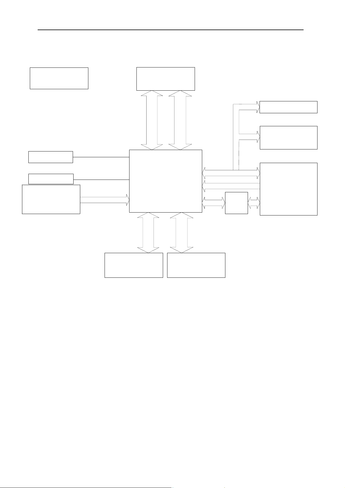
Block Diagram
Linear regulators for
CPU & FPGA cores
4 LEDs &
4 I/O pins
JTAG Header
Sundance High-speed Bus
(60-way Samtec)
Sundance Digital Bus
(40-way ODU)
83 I/O
J1 Top Primary TIM
FPGA Controller
Spartan-IIE, FG456
Global Bus
J3 Global Expansion
Connector
Connector
Comm-Port 0 & 3
24 I/O pins
2x Comm-Ports/SDL
329 I/O Pins
XC2S300E
1.5V
74 I/O pins
J2 Bottom Primary TIM
15 I/O pins
Timer,& Control
24 I/O pins
2x Comm-Port/SDL
Connector
Comm-Port 1 & 4
(2 linked with 5)
TTL I/O
64 pins
McBSP
McBSP &
GPIO
Header
Flash (CE1)
Start-up mode selection.
256M bytes SDRAM (CE2,3)
8 x K4S560832
(32M x 8)
'C6711/6713
DSP
Architecture Description
The SMT376 TIM consists of a Texas Instruments TMS320C6211/6711/6713 running
at up to 225MHz. Modules are populated with 256MBytes of synchronous DRAM
(SDRAM).
A Field Programmable Gate Array (FPGA) is used to manage global bus accesses
and implement four communication ports and Sundance Digital/High-speed Buses.
This is a Xilinx Spartan –IIE device.
Page 8

Version 1.7 Page 8 of 24 SMT376 User Manual
TMS320C6211/6711
The processor will run with zero wait states from internal SRAM. The internal memory
is 64k bytes in size and can be partitioned between normal SRAM and/or L2 cache.
An on-board crystal oscillator provides the clock used for the C60 which then
multiplies this by 4 internally.
Boot Mode
The SMT376 is configured to use the following boot sequence each time it is taken
out of reset:
1. The processor copies a bootstrap program from the first part of the flash
memory into internal program RAM starting at address 0.
2. Execution starts at address 0.
The standard bootstrap supplied with the SMT376 then performs the following
operations:
1. All relevant C60 internal registers are set to default values;
2. The FPGA is configured from data held in flash memory and sets up the
communication ports, the global bus and the Sundance Digital/High-speed
Buses. This step must have been completed before data can be sent to the
ComPorts from external sources such as the host or other TIMs;
3. A C4x-style boot loader is executed. This will continually examine the four
communication ports until data appears on one of them. The bootstrap will
then load a program in boot format from that port; the loader will not read data
arriving on other ports. See “Application Development” for details of the boot
loader format;
4. Finally, control is passed to the loaded program.
Page 9

Version 1.7 Page 9 of 24 SMT376 User Manual
The delay between the release of the board reset and the FPGA configuration is
around 0.5s for a SMT376 (150MHz clock).
A typical time to wait after releasing the board reset should be in excess of this delay,
but no damage will result if any of the I/Os are used before they are fully configured.
In fact, the ComPorts will just produce a not ready signal when data is attempted to
be transferred during this time, and then continue normally after the FPGA is
configured.
EMIF Control Registers
The C60 has a single external memory interface (EMIF) which is 32 bits wide.
The C60 contains several registers that control the external memory interface (EMIF).
A full description of these registers can be found in the C60 Peripherals Reference
Guide.
The standard bootstrap will initialise these registers to use the following resources:
Memory space
(EMIF)
Resource Address range
CE0 Spartan 0x80000000 - 0x8FFFFFFF
CE1 Flash 0x90000000 - 0x901FFFFF
CE2 SDRAM bank 0 0xA0000000 - 0xA7FFFFFF
CE3 SDRAM bank 1 0xB0000000 - 0xB7FFFFFF
SDRAM
Memory spaces CE2 & 3 are used to access 256MB of SDRAM over the EMIF.
The speed of the SDRAM is dependant on the processor variant. Using the C6x11,
the SDRAM will operate at 100MHz.
Using the C6713, the SDRAM operates at a programmable rate up to the maximum
allowed on the EMIF (TI data sheet = TBD).
The EMIF CE2 & 3 memory space control registers should be programmed with the
value 0x00000030.
Page 10

Version 1.7 Page 10 of 24 SMT376 User Manual
FLASH
A 2MByte Flash ROM device is connected to the C60 EMIF CE1 memory space.
The ROM holds boot code for the C60, configuration data for the FPGA, and optional
user-defined code.
A software protection algorithm is in place to prevent programs accidentally altering
the ROM’s contents. Please contact Sundance for further information about reprogramming this device.
The CE1 memory space control register should be programmed with the value
0x105FFF23.
Version control
Revision numbers for both the boot code and FPGA firmware are stored in the Flash
ROM during programming as zero-terminated ASCII strings.
The SMT6001 utility is to be used to know the version of the boot code and the
FPGA.
Reprogramming the firmware and boot code
The reprogramming is made using the SMT6001 utility. It comes with the latest
firmware and boot code for the module and with a complete documentation on how to
reprogram a module. It requires only the correct set-up for code composer (see code
composer section).
To confirm that the programming has been successful you should use the Sundance
Server to reset the board and execute the confidence test using SMTBoardInfo.
Interrupts
See general firmware description
Communication ports
The SMT376 provides 4 ComPorts. They are ComPorts 0, 1, 3 and 4.
ComPorts 2 and 5 are interconnected on the module to allow a bypass to the next
module.
See general firmware description
Page 11

Version 1.7 Page 11 of 24 SMT376 User Manual
SDB
The SMT376 provides two Sundance Digital Buses (SDBs). These 16-bit data
parallel links for synchronous transmission can achieve high-speed data transfer
across 40-way flat ribbon cables with ground-interlaced 3.3v signals (Ref. SMT3xxSDB-CAB) and Samtec QSH/QTH based cable designs.
The SDB connector carries one 16 bits SDB bus (SDB0).
The SHB connector carries one 16 bits SDB bus (SDB1). The second 16 SDB is not
implemented.
See general firmware description
SDB Clock selection
In this firmware the SDB clock is not selectable and is fixed at 100MHz.
Changing the bit SDBCLK will have no effect
Global bus
The SMT335 provides one global bus interface.
See general firmware description
Page 12

Version 1.7 Page 12 of 24 SMT376 User Manual
LED Setting
The SMT376 has 5 LEDs.
LED D6 always displays the state of the FPGA DONE pin. This LED is off when the
FPGA is configured (DONE=1) and on when it is not configured (DONE=0).
This LED should go on when the board is first powered up and go off when the FPGA
has been successfully programmed (this is the standard operation of the boot code
resident in the flash memory device). If the LED does not light at power-on, check
that you have the mounting pillars and screws fitted properly. If it stays on, the DSP
is not booting correctly, or is set to boot in a non-standard way.
Four of the remaining LEDs can be controlled with the LED register. Writing 1 will
illuminate the LED; writing 0 will turn it off.
LED Register
31–4 3 2 1 0
LED D5 LED D4 LED D3 LED D2
RW,0 RW,0 RW,0 RW,0
CONFIG & NMI
See general firmware description
Timer
See general firmware description
IIOF interrupt
The firmware can generate pulses on the external interrupt lines of the TIM.
See general firmware description
Code Composer
This module is fully compatible with the Code Composer Studio debug and
development environment. This extends to both the software and JTAG debugging
hardware. The driver to with the SMT376 use is tixds6x1x.dvr. Code composer V2.2
is required for the SMT6001 to work.
Page 13

Version 1.7 Page 13 of 24 SMT376 User Manual
Application Development
You can develop code for SMT376 modules in several ways. The simplest is to use
the Sundance SMT6000 Server Loader and its associated libraries (shortly to be
discontinued).
The Server Loader is an application that runs on a host PC under either Windows 98,
2000 or NT and allows you to run COFF-format applications. Modified forms of the TI
RTS library support standard C I/O.
The Server Loader will read a .out file and convert it into C4x-style boot code which
is then transmitted down a ComPort to the SMT376.
The boot code is in the following format:
1
Word
1 0 reserved
6-word
header
Words 2, 3, 4 0, 0, 0
Word 5 start address
Word 6 0
Word 1 4*N: Length of load block (in bytes)2
Load Block
Word 2 Destination address (external memory only)
Next N words N data words
0 or more
Load Blocks
Terminator Word 1 03
1
A word is 32 bits
2
The length of each data block will be rounded up to a multiple of 4 bytes if necessary.
3
Effectively a zero-length Load Block
Page 14

Version 1.7 Page 14 of 24 SMT376 User Manual
Operating Conditions
Safety
The module presents no hazard to the user.
EMC
The module is designed to operate within an enclosed host system that provides
adequate EMC shielding. Operation within the EU EMC guidelines is only guaranteed
when the module is installed within an appropriate host system.
The module is protected from damage by fast voltage transients introduced along
output cables from outside the host system.
Short-circuiting any output to ground does not cause the host PC system to lock up
or reboot.
General Requirements
The module must be fixed to a TIM40-compliant carrier board.
The SMT376 TIM is in a range of modules that must be supplied with a 3.3v power
source. In addition to the 5v supply specified in the TIM specification, these new
generation modules require an additional 3.3v supply to be presented on the two
diagonally-opposite TIM mounting holes. The lack of this 3.3v power supply should
not damage the module, although it will obviously be inoperable; prolonged operation
under these circumstances is not recommended.
This module is not directly compatible with earlier generations of TIM motherboards,
although the 3.3v supply can be provided from a separate source. It is, however,
compatible with the latest generation of Sundance TIM carrier boards such as the
SMT310Q and subsequent versions (PCI), and SMT328 (VME), which present the
3.3v via conductive mounting pillars.
Use of the TIM on SMT327 (cPCI) motherboards may require a firmware upgrade. If
LED D6 on the SMT376 remains illuminated once the TIM is plugged in and powered
up, the SMT327 needs the upgrade. The latest firmware is supplied with all new
boards shipped. Please contact Sundance directly if you have an older board and
need the upgrade.
The external ambient temperature must remain between 0°C and 40°C, and the
relative humidity must not exceed 95% (non-condensing).
Power Consumption
The power consumption of this TIM is dependent on the operating conditions in terms
of core activity and I/O activity. The maximum power consumption is 3W.
Page 15

Version 1.7 Page 15 of 24 SMT376 User Manual
Connector Positions
Page 16

Version 1.7 Page 16 of 24 SMT376 User Manual
Virtex Memory Map
See general firmware description with i = 14
The memory mapping is as follows:
#define CP0 (volatile unsigned int *)0x80000000
#define CP1 (volatile unsigned int *)0x80008000
#define CP3 (volatile unsigned int *)0x80018000
#define CP4 (volatile unsigned int *)0x80020000
#define CP0_STAT (volatile unsigned int *)0x80004000
#define CP1_STAT (volatile unsigned int *)0x8000C000
#define CP3_STAT (volatile unsigned int *)0x8001C000
#define CP4_STAT (volatile unsigned int *)0x80024000
#define GBSTAT (volatile unsigned int *)0x80034000
#define SDBSTAT (volatile unsigned int *)0x80038000
#define STAT (volatile unsigned int *)0x8003C000
#define SDBA (volatile unsigned int *)0x80040000
#define SDBB (volatile unsigned int *)0x80050000
#define SDBA_STAT (volatile unsigned int *)0x80048000
#define SDBB_STAT (volatile unsigned int *)0x80058000
#define SDBA_INPUTFLAG (volatile unsigned int *)0x80044000
#define SDBB_ INPUTFLAG (volatile unsigned int *)0x80054000
#define SDBA_OUTPUTFLAG (volatile unsigned int *)0x8004C000
#define SDBB_OUTPUTFLAG (volatile unsigned int *)0x8005C000
#define GLOBAL_BUS (volatile unsigned int *)0x800A0000
#define GLOBAL_BUS_CTRL (volatile unsigned int *)0x80080000
#define GLOBAL_BUS_START (volatile unsigned int *)0x80088000
#define GLOBAL_BUS_LENGTH (volatile unsigned int *)0x80090000
#define TCLK (volatile unsigned int *)0x800C0000
#define TIMCONFIG (volatile unsigned int *)0x800C8000
#define LED (volatile unsigned int *)0x800D0000
#define IIOF (volatile unsigned int *)0x800D8000
#define INTCTRL4 (volatile unsigned int *)0x800E0000
#define SDBINTCTRL4 (volatile unsigned int *)0x800E4000
#define INTCTRL5 (volatile unsigned int *)0x800E8000
#define SDBINTCTRL5 (volatile unsigned int *)0x800EC000
#define INTCTRL6 (volatile unsigned int *)0x800F0000
#define SDBINTCTRL6 (volatile unsigned int *)0x800F4000
#define INTCTRL7 (volatile unsigned int *)0x800F8000
Page 17

Version 1.7 Page 17 of 24 SMT376 User Manual
#define SDBINTCTRL7 (volatile unsigned int *)0x800FC000
Page 18

Version 1.7 Page 18 of 24 SMT376 User Manual
Connector Pin-outs
SDB0 Pin-Out
Pin Signal Signal Pin
1 CLK GND 2
3 D0 GND 4
5 D1 GND 6
7 D2 GND 8
9 D3 GND 10
11 D4 GND 12
13 D5 GND 14
15 D6 GND 16
17 D7 GND 18
19 D8 GND 20
21 D9 GND 22
23 D10 GND 24
25 D11 GND 26
27 D12 GND 28
29 D13 GND 30
31 D14 GND 32
33 D15 GND 34
35 UD0 DIR 36
37 WEN REQ 38
39 UD1 ACK 40
FPGA JTAG
The following shows the pin-outs for JP4 (FPGA) JTAG connector:
Signal Pin Pin Signal
V33 1 2 TCK
GND 3 4 TMS
TDO 5 6 TDI
Page 19

Version 1.7 Page 19 of 24 SMT376 User Manual
SHB pin-out
Pin Signal Signal Pin
1
3
5
7
9
11
13
15
17
19
21
23
25
27
29
SDB1_CLK SDB1_D0
SDB1_D1 SDB1_D2
SDB1_D3 SDB1_D4
SDB1_D5 SDB1_D6
SDB1_D7 SDB1_D8
SDB1_D9 SDB1_D10
SDB1_D11 SDB1_D12
SDB1_D13 SDB1_D14
SDB1_D15 SDB1_U0
SDB1_U1 -
- SDB1_WEN1
SDB1_REQ1 SDB1_ACK1
- -
- -
- -
2
4
6
8
10
12
14
16
18
20
22
24
26
28
30
31
33
35
37
39
41
43
45
47
49
51
53
55
57
59
- -
- -
- -
SDB2_CLK SDB2_D0
SDB2_D1 SDB2_D2
SDB2_D3 SDB2_D4
SDB2_D5 SDB2_D6
SDB2_D7 SDB2_D8
SDB2_D9 SDB2_D10
SDB2_D11 SDB2_D12
SDB2_D13 SDB2_D14
SDB2_D15 SDB2_U0
SDB2_U1 -
- SDB2_WEN
SDB2_REQ SDB2_ACK
32
34
36
38
40
42
44
46
48
50
52
54
56
58
60
Not implemented
Page 20

Version 1.7 Page 20 of 24 SMT376 User Manual
This standard is implemented using SAMTEC QSTRIP 0.50mm Hi-speed connectors.
To improve electrical performances, a ground plane is embedded in each QSTRIP
connector.
For long distances micro-coax ribbon cable is used to connect 2 QSTRIP connectors.
Page 21

Version 1.7 Page 21 of 24 SMT376 User Manual
Serial Ports & Other C60 I/O (EXP connector)
The C60 contains various I/O ports. These signals are connected to a QSH type
connector. The pin-out of this connector is shown here:
Pin
number
1 HPI CS HPI HDS1 2
3 HPI RDY HPI HDS2 4
5 HPI CNTRL0 HPI CNTRL1 6
7 HPI HWIL HPI RW 8
9 HPI AS GND 10
11 3.3V GND 12
13 HPI D0 HPI D8 14
15 HPI D1 HPI D9 16
17 HPI D2 HPI D10 18
19 HPI D3 HPI D11 20
21 HPI D4 HPI D12 22
23 HPI D5 HPI D13 24
25 HPI D6 HPI D14 26
27 HPI D7 HPI D15 28
29 HPI INT GND 30
Signal Signal Pin
number
31 3.3V DSP GPIO2 32
33 3.3V GND 34
35 FPGA TTL0 FPGA TTL2 36
37 FPGA TTL1 FPGA TTL3 38
39 N/C N/C 40
41 N/C N/C 42
43 N/C N/C 44
45 N/C N/C 46
47 MCBSP CLKS1 MCBSP CLKS0 48
49 MCBSP CLKR1 MCBSP CLKR0 50
51 MCBSP CLKX1 MCBSP CLKX0 52
53 MCBSP DR1 MCBSP DR0 54
55 MCBSP DX1 MCBSP DX0 56
57 MCBSP FSR1 MCBSP FSR0 58
59 MCBSP FSX1 MCBSP FSX0 60
Page 22

Version 1.7 Page 22 of 24 SMT376 User Manual
Serial Ports & Other C60 I/O (JP3 connector)
Pin
number
1 MCBSP CLKS1 MCBSP CLKR1 2
3 MCBSP CLKX1 MCBSP DR1 4
5 MCBSP DX1 MCBSP FSR1 6
7 MCBSP FSX1 GND 8
9 MCBSP CLKS0 MCBSP CLKR0 10
11 MCBSP CLKX0 MCBSP DR0 12
13 MCBSP DX0 MCBSP FSR0 14
15 MCBSP FSX0 3.3V 16
17 FPGA TTL0 FPGA TTL1 18
19 FPGA TTL2 FPGA TTL3 20
21 DSP GPIO0 DSP GPIO1 22
23 DSP GPIO2 DSP GPIO3 24
25 GND GND 26
Signal Signal Pin
number
FPGA PROG Pin Control (JP2 connector)
Jumper Position
1-2 2-3 Out
PROG asserted
continuously
PROG asserted for the
duration of RESET.
Can also be controlled
by the DSP.
DSP JTAG Control (JP1 connector)
In JTAG enabled to DSP
Out JTAG enabled to DSP only after the
DSP reads the flash
PROG under control of
DSP
Page 23

Version 1.7 Page 23 of 24 SMT376 User Manual
Data Sheets (Hyperlinks)
1. TMS320C6211/C6711 Peripherals Reference Guide (literature number SPRU190)
http://www-s.ti.com/sc/psheets/spru190e/spru190e.pdf
Describes common peripherals available on the TMS320C6211/C6711 digital signal processors.
This book includes information on the internal data and program memories, the external memory
interface (EMIF), the host port, multichannel-buffered serial ports, direct memory access (EDMA),
clocking and phase-locked loop (PLL), and the power-down modes.
2. SMT6001 http://www.sundance.com/edge/files/productpage.asp?STRfilter=smt6001
3. TIM-40 MODULE SPECIFICATION Including TMS320C44 Addendum
ftp://ftp2.sundance.com/Pub/documentation/pdf-files/tim_spec_v1.01.pdf
4. SDB Technical Specification
http://www.sundance.com/edge/files/productpage.asp?STRfilter=sdb
5. SHB Technical Specification
http://www.sundance.com/edge/files/productpage.asp?STRfilter=shb
6. TMS320C4x User's Guide (literature number SPRU063)
http://www-s.ti.com/sc/psheets/spru063c/spru063c.pdf
Describes the C4x 32-bit floating-point processor, developed for digital signal processing as well
as parallel processing applications. Covered are its architecture, internal register structure,
instruction set, pipeline, specifications, and operation of its six DMA channels and six
communication ports. Software and hardware applications are included.
7. Xilinx Spartan-IIE data sheet:
http://www.xilinx.com/partinfo/ds077.htm
8. Texas Instruments TMS320C6211B data sheet:
http://www-s.ti.com/sc/ds/tms320c6211b.pdf
9. Texas Instruments TMS320C6711 data sheet:
http://www-s.ti.com/sc/ds/tms320c6711b.pdf
Page 24

Version 1.7 Page 24 of 24 SMT376 User Manual
Index
Application Development...............13
server-loader.................................13
Architecture Description..................7
Block Diagram ..................................7
Board not working
firmware revision.............................3
LED 6 illuminated..........................12
no 3.3v supply...............................14
boot code format ............................13
Boot Mode.........................................8
bootstrap program ...........................8
carrier boards .................................14
Code Composer..............................12
Contacting Sundance.......................4
Data Sheets (Hyperlinks) ...............23
EMIF Control Registers....................9
field values after reset......................5
Flash ................................................10
protection algorithm ......................10
FPGA .................................................7
configuration ...................................8
LEDs ................................................12
FPGA DONE pin ...........................12
memory space (CE0 to CE3)........... 9
motherboards................................. 14
NMI .................................................. 12
Notational Conventions .................. 5
Operating Conditions .................... 14
Power
3.3v .............................................. 14
power consumption ...................... 14
register descriptions ....................... 5
revision numbers
boot code ..................................... 10
FPGA firmware............................. 10
SDB ................................................. 11
cables........................................... 11
clock speed .................................. 11
SDRAM ............................................. 9
Serial Ports................................21, 22
SMT376 ............................................. 5
Sundance TIM carrier boards ....... 14
Timer............................................... 12
TMS320C6711................................... 8
Virtex
memory map ................................ 16
LED register ..................................12
 Loading...