

Page 1

SMT365G
User Manual
User Manual (QCF42); Version 3.0, 5/2/01; © Sundance Multiprocessor Technology Ltd. 2001
Page 2
Version 1.0.0 Page 2 of 23 SMT365G User Manual
Revision History
Date Comments Engineer Version
23/09/04 First rev, based on 365 user manual (v1.1.3) J.V. 1.0.0
Page 3

Version 1.0.0 Page 3 of 23 SMT365G User Manual
Table of Contents
Revision History ....................................................................................................... 2
Contacting Sundance............................................................................................... 4
Notational Conventions ................................................Error! Bookmark not defined.
C60 ......................................................................................................................... 4
SDB ........................................................................................................................ 4
Register Descriptions.............................................................................................. 4
Outline Description .................................................................................................. 6
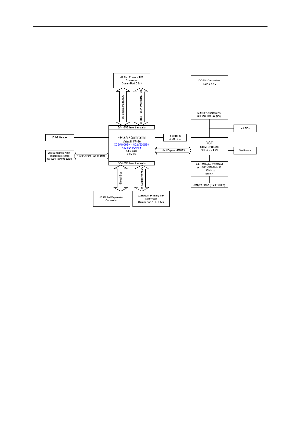
Architecture Description.......................................................................................... 7
TMS320C6416 ........................................................................................................... 8
Boot Mode............................................................................................................... 8
Flash Boot.......................................................................................................... 8
HPI Boot ............................................................................................................. 8
EMIF Control Registers........................................................................................... 9
ZBTRAM ............................................................................................................... 10
FLASH .................................................................................................................. 10
Virtex FPGA ..................................................................................................... 11
Reprogramming the firmware and boot code ...................................................... 12
Interrupts................................................................................................................. 13
Interrupts................................................................................................................. 13
SDL/Communication ports .................................................................................... 13
SHB.......................................................................................................................... 13
SHB-Half Word (16-bits SDB) firmware version.................................................... 13
SDB Clock selection .......................................................................................... 13
SHB-Word (SHB32x) firmware version ....................Error! Bookmark not defined.
Compatibility 16/32 bits ........................................Error! Bookmark not defined.
SDB Clock selection.............................................Error! Bookmark not defined.
Global bus............................................................................................................... 14
LED Setting ............................................................................................................. 14
CONFIG & NMI ........................................................................................................ 14
Timer........................................................................................................................ 14
IIOF interrupt........................................................................................................... 14
Page 4

Version 1.0.0 Page 4 of 23 SMT365G User Manual
FPGA space availability ......................................................................................... 15
Code Composer...................................................................................................... 15
Application Development..............................................Error! Bookmark not defined.
Operating Conditions............................................................................................. 15
Safety.................................................................................................................... 15
EMC...................................................................................................................... 15
General Requirements.......................................................................................... 16
Power Consumption.............................................................................................. 16
Weight................................................................................................................... 16
Connector Positions .............................................................................................. 17
Serial Ports & Other C60 I/O .................................................................................. 18
FPGA and CPLD JTAG........................................................................................... 18
Virtex Memory Map................................................................................................. 19
SHB pin-out............................................................................................................. 21
16-bits SDB interface: ..............................................Error! Bookmark not defined.
32-bits SDB interface: ..............................................Error! Bookmark not defined.
FPGA Pin-Out.................................................................Error! Bookmark not defined.
Bibliography............................................................................................................ 22
Index ........................................................................................................................ 23
Contacting Sundance
You can contact Sundance for additional information by login onto the support
system
C60
The terms C60, C64xx and TMS320C64xx will be used interchangeably throughout
this document.
SDB
support.sundance.com
The term SDB will be used throughout this document to refer to a 16 bit data bus
carried by either an SDB connector or an SHB connector. The SHB connector can
carry two such SDB buses.
Register Descriptions
Page 5

Version 1.0.0 Page 5 of 23 SMT365G User Manual
The format of registers is described using diagrams of the following form:
31–24 23–16 15–8 7–0
OFLAGLEVEL
R,00000000 RW,10000000 R,00000000 R,10000000
The digits at the top of the diagram indicate bit positions within the register and the
central section names bits or bit fields. The bottom row describes what may be done
to the field and its value after reset. Shaded fields are reserved and should only ever
be written with zeroes.
R Readable by the CPU
W Writeable by the CPU
RW Readable and writeable by the CPU
Binary digits indicate the value of the field after reset.
Page 6

Version 1.0.0 Page 6 of 23 SMT365G User Manual
Outline Description
The SMT365G is a C64xx-based size 1 TIM offering the following features:
TMS320C6416T processor running at 1GHz
Six 20MB/s communication ports (ComPort)
8MB of ZBTRAM (133MHz)
8MByte Flash ROM for boot code and FPGA programming
Global expansion connector
High bandwidth data I/O via Sundance Digital Buses (SDB) or Sundance High
Speed Buses (SHB).
Page 7
Version 1.0.0 Page 7 of 23 SMT365G User Manual
Block Diagram
Architecture Description
The SMT365G TIM consists of a Texas Instruments TMS320C6416T running at up to
1GHz. Modules are populated with 8MBytes of zero bus turnaround RAM (ZBTRAM).
A Field Programmable Gate Array (FPGA) is used to manage global bus accesses
and implement six communication ports and four Sundance Digital Buses. This is a
Xilinx VirtexII device.
Page 8

Version 1.0.0 Page 8 of 23 SMT365G User Manual
TMS320C6416T
The processor will run with zero wait states from internal SRAM.
An on-board crystal oscillator provides the clock used for the C60 which then
multiplies this by 12 internally.
Boot Mode
The SMT365G can be configured to use one of two boot modes after a reset. These
are HPI (host port interface) and Flash.
Flash Boot
1. The processor copies a bootstrap program from the first part of the flash
memory into internal program RAM starting at address 0.
2. Execution starts at address 0.
The standard bootstrap supplied with the SMT365G then performs the following
operations:
1. All relevant C60 internal registers are set to default values;
2. The FPGA is configured from data held in flash memory and sets up the
communication ports, the global bus and the Sundance High-speed Buses.
This step must have been completed before data can be sent to the commports from external sources such as the host or other TIMs;
3. A C4x-style boot loader is executed. This will continually examine the six
communication ports until data appears on one of them. The bootstrap will
then load a program in boot format from that port; the loader will not read data
arriving on other ports.
4. Finally, control is passed to the loaded program.
The delay between the release of the board reset and the FPGA configuration is
around 1s for a SMT365G (600MHz clock).
A typical time to wait after releasing the board reset should be in excess of this
delay, but no damage will result if any of the I/Os are used before they are fully
configured. In fact, the comm. Ports will just produce a not ready signal when data
transfer is attempted during this time, and then continue normally after the FPGA
is configured.
HPI Boot
The C60’s HPI (16 bit data interface) is connected directly to the FPGA. This
mode is therefore only used by custom FPGA configurations.
Page 9

Version 1.0.0 Page 9 of 23 SMT365G User Manual
EMIF Control Registers
The C6416T has two external memory interfaces (EMIFs). One of these is 64 bits
wide, the other 16 bits.
The C60 contains several registers that control the external memory interfaces
(EMIFs). A full description of these registers can be found in the C60 Peripherals
Reference Guide[0].
The standard bootstrap will initialise these registers to use the following
resources:
Memory
space
Resource Address range
(EMIFA)
Internal program memory
0x00000000 - 0x000FFFFF
(1Mbyte)
CE0 ZBTRAM (8Mbytes) 0x80000000 - 0x807FFFFF
CE1 Virtex 0x90000000 - 0x900FFFFF
Memory
space
Resource Address range
(EMIFB)
CE1 1st / 3rd section of flash
0x67E00000 – 0x67FFFFFF
(2Mbyte each)
CE2 2nd / 4th section of flash
0x68000000 – 0x681FFFFF
(2Mbyte each)
Page 10

Version 1.0.0 Page 10 of 23 SMT365G User Manual
ZBTRAM
Memory space CE0 is used to access 8MB of ZBTRAM over EMIFA. The ZBTRAM
operates at the external oscillator frequency of 133MHz.
The EMIFA CE0 memory space control register should be programmed with the
value 0x000000E0.
Note that the DSP only has 20 address pins on the EMIFA and cannot therefore
directly address more than 8Mbytes of SRAM (the ZBTRAM is a type of SRAM with
non-multiplexed address pins).
FLASH
An 8MByte Flash ROM device is connected to the C60 EMIFB.
The ROM holds boot code for the C60, configuration data for the FPGA, and optional
user-defined code.
The EMIFB CE1 and CE2 space control registers should be programmed with the
value 0xFFFFFF03.
As the C60 only provides 20 address lines on its EMIFB, both CE1 & CE2 are used
to access this device. This in itself allows the direct access of 4Mbytes. A paging
mechanism is used to select which half of the 8M device is visible in this 4Mbyte
window.
As the EMIFB CE1 & 2 memory spaces alias throughout the available range, the
flash device can be accessed using the address range 0x67E00000-0x681FFFFF.
This gives a 4Mbyte continuous space.
The flash can be divided into the four logical sections shown in the following figure
(paging bit is bit 21).
Page0
(2 MBytes)
CE1
Page1
(2 MBytes)
Page0
(2 MBytes)
CE2
Page1
(2 MBytes)
0x67C00000
Section 1
0x67E00000
Section 2
0x68000000
Section 3
0x68200000
Section 4
0x68400000
Figure 1: Flash logical sections
To change the state of the page bit, you need to write to the following address as
shown (the data written is irrelevant):
Page 11

Version 1.0.0 Page 11 of 23 SMT365G User Manual
Address Flash page selected
0x6C000000 Page 0 (1st and 3rd
sections enabled)
0x6C000001 Page 1 (2nd and 4th
sections enabled)
The EMIFB CE3 space control register should be programmed with the value
0xFFFFFF03.
This mechanism is identical in operation to that needed for the largest ZBTRAMs.
Virtex FPGA
The SMT365G incorporates a Xilinx Virtex XC2V1000 FPGA. This device controls
the majority of the I/O functionality on the module, including the comm ports, SHBs
and global bus.
This device requires configuring after power-up (the Virtex technology is an SRAM
based logic array). This configuration is performed by the DSP as part of the boot
process.
Two control register bits are needed for this purpose, one to put the FPGA into a
‘waiting for configuration’ state, and another to actually transfer the configuration
data.
The PROG pin (causes the FPGA to enter the non-configured state) is accessed at
address 0x6C02000X. Writing to address 0x6C020000 will assert this pin, and
address 0x6C0200001 will de-assert this pin.
The configuration data clock is accessed at address 0x6C080001. Each bit of the
FPGA’s configuration bit-stream must be serially clocked through this address.
Note: This configuration process is part of the standard boot code, and does not
need to be implemented in any user application.
Page 12

Version 1.0.0 Page 12 of 23 SMT365G User Manual
Reprogramming the firmware and boot code
Please refer to the following documentation:
http://www.sundance.com/docs/SMT6001%20User%20Manual.pdf
Page 13

Version 1.0.0 Page 13 of 23 SMT365G User Manual
Interrupts
See general firmware description [7]
SDL/Communication ports
The SMT365G provides 6 ComPorts. They are ComPort 0, 1, 2, 3, 4 and 5.
SMT365G implements only ComPort interface.
SHB
SMT365G’s firmware is available in 1 version:
• SHB-Half Word (16-bits SDB) firmware version.
See SHB [4] or SDB [3] technical specifications and general firmware description [7]
for more details.
SHB-Half Word (16-bits SDB) firmware version
This configuration of the SMT365G provides four Sundance Digital Buses(SDB).
They are numbered SDB0 for SDBA, SDB1 for SDBB, SDB2 for SDBC, SDB3 for
SDBD.
SDBC
SDBA
SDBD
SDBB
SDB Clock selection
The SDB clock selection is not available. The SDB runs at 100Mhz. This clock is
provided by an on-board oscillator.
Altering SDBCLK value won’t have any effect.
Page 14

Version 1.0.0 Page 14 of 23 SMT365G User Manual
Global bus
The SMT365G provides one global bus interface.
See general firmware description [7]
LED Setting
The SMT365G has 9 LEDs.
LED D6 always displays the state of the FPGA DONE pin. This LED is off when the
FPGA is configured (DONE=1) and on when it is not configured (DONE=0).
This LED should go on when the board is first powered up and go off when the FPGA
has been successfully programmed (this is the standard operation of the boot code
resident in the flash memory device). If the LED does not light at power-on, check
that you have the mounting pillars and screws fitted properly. If it stays on, the DSP
is not booting correctly, or is set to boot in a non-standard way.
Four of the LEDs (D7-10) can be controlled with the LED register. Writing 1 will
illuminate the LED; writing 0 will turn it off.
Currently the SMT365G only implements 2 of these leds D7 and D8.
LED Register
LED 0x900D0000
31–4 3 2 1 0
LED
D10
RW,0 RW,0 RW,0 RW,0
LED
D9
LED
D8
LED
D7
The four remaining LEDs (D2-5) are connected to the C60’s GPIO pins 12-15.
CONFIG & NMI
See general firmware description [7]
Timer
See general firmware description [7]
IIOF interrupt
The firmware can generate pulses on the external interrupt lines of the TIM.
See general firmware description [7]
Page 15

Version 1.0.0 Page 15 of 23 SMT365G User Manual
FPGA space availability
The firmware is generated with Xilinx ISE.
Table below gives the device utilization summary after placing and routing the
firmware:
XST
SMT365G
Yes
compatible
Number of
40% (16)
RAMB16s
Number of
44% (2289)
SLICEs
Number of
12% (2)
BUFGMUXs
Number of
30% (780)
TBUFs
Code Composer
This module is fully compatible with the Code Composer Studio (CCS) debug
environment (version 2 or later). This extends to both the software and JTAG
debugging hardware.
The name of the C64xx CCS device driver is tixds64xx_11.dvr, and should be
obtained from Texas Instruments. In case of difficulty please contact
support.sundance.com
Operating Conditions
Safety
The module presents no hazard to the user.
EMC
The module is designed to operate within an enclosed host system that provides
adequate EMC shielding. Operation within the EU EMC guidelines is only guaranteed
when the module is installed within an appropriate host system.
The module is protected from damage by fast voltage transients introduced along
output cables from outside the host system.
Short-circuiting any output to ground does not cause the host PC system to lock up
or reboot.
Page 16

Version 1.0.0 Page 16 of 23 SMT365G User Manual
General Requirements
The module must be fixed to a TIM40-compliant carrier board.
The SMT365G TIM is in a range of modules that must be supplied with a 3.3v power
source. In addition to the 5v supply specified in the TIM specification, these new
generation modules require an additional 3.3v supply to be presented on the two
diagonally-opposite TIM mounting holes. The lack of this 3.3v power supply should
not damage the module, although it will obviously be inoperable; prolonged operation
under these circumstances is not recommended.
The SMT365G is compatible with all Sundance TIM carrier boards. It is a 5v tolerant
module, and as such, it may be used in mixed systems with older TIM modules,
carrier boards and I/O modules.
Use of the TIM on SMT327 (cPCI) motherboards may require a firmware upgrade. If
LED D6 on the SMT365G remains illuminated once the TIM is plugged in and
powered up, the SMT327 needs the upgrade. The latest firmware is supplied with all
new boards shipped. Please contact Sundance directly if you have an older board
and need the upgrade.
The external ambient temperature must remain between 0°C and 40°C, and the
relative humidity must not exceed 95% (non-condensing).
Power Consumption
The power consumption of this TIM is dependent on the operating conditions in terms
of core activity and I/O activity. The maximum power consumption is 10W.
Weight
SMT365G weigh approximately 56.25 grams.
Page 17

Version 1.0.0 Page 17 of 23 SMT365G User Manual
Connector Positions
Page 18

Version 1.0.0 Page 18 of 23 SMT365G User Manual
Serial Ports & Other C60 I/O
The C60 contains various I/O ports. These signals are connected to a 0.1” pitch DIL
pin header. The pin-out of this connector is shown here:
P O TTL1 TTL0 GND GND GPIO7 GPIO6 GPIO5 GPIO4 GPIO3 GPIO2
CLK / 6
L A TTL3 TTL2 V33 V33 GPIO15 GPIO14 GPIO13 GPIO12 GPIO11 GPIO10 GPIO9 NC
R I URD0 URD1 URD2 URD3 URD4 URD5 URD6 URD7 URCLK URENB URCLAV URSOC
S A UXD0 UXD1 UXD2 UXD3 UXD4 UXD5 UXD6 UXD7 UXCLK UXENB UXCLAV UXSOC
GPIO1
CLK / 4
GPIO0
T I UXA0 DR1
UXA1
O N URA0 URA1 CLKR1
FSR1
UXA2
URA2
FSX1
UXA3
CLKX1
URA4
DX1
UXA4
CLKS1
URA3
CLKS2
GPIO8
CLKS0 CLKX0 CLKR0 FSX0 DX0 FSR0 DR0
CLKX2 CLKR2 FSX2 DX2 FSR2 DR2
FPGA and CPLD JTAG
The following shows the pin-outs for JP2 (CPLD) and JP3 (FPGA) JTAG connectors:
Signal Pin Pin Signal
V33 1 2 TMS
TCK 3 4 TDO
GND 5 6 TDI
Page 19

Version 1.0.0 Page 19 of 23 SMT365G User Manual
Virtex Memory Map
See general firmware description.
The memory mapping is as follows:
#define SMT365CP0 (volatile unsigned int *)0x90000000
#define SMT365CP1 (volatile unsigned int *)0x90008000
#define SMT365CP2 (volatile unsigned int *)0x90010000
#define SMT365CP3 (volatile unsigned int *)0x90018000
#define SMT365CP4 (volatile unsigned int *)0x90020000
#define SMT365CP5 (volatile unsigned int *)0x90028000
#define SMT365CP0_STAT (volatile unsigned int *)0x90004000
#define SMT365CP1_STAT (volatile unsigned int *)0x9000C000
#define SMT365CP2_STAT (volatile unsigned int *)0x90014000
#define SMT365CP3_STAT (volatile unsigned int *)0x9001C000
#define SMT365CP4_STAT (volatile unsigned int *)0x90024000
#define SMT365CP5_STAT (volatile unsigned int *)0x9002C000
#define SMT365GB_STAT (volatile unsigned int *)0x90034000
#define SMT365SDB_STAT (volatile unsigned int *)0x90038000
#define SMT365STAT (volatile unsigned int *)0x9003C000
#define SMT365SDBA (volatile unsigned int *)0x90040000
#define SMT365SDBB (volatile unsigned int *)0x90050000
#define SMT365SDBC (volatile unsigned int *)0x90060000
#define SMT365SDBD (volatile unsigned int *)0x90070000
#define SMT365SDBA_STAT (volatile unsigned int *)0x90048000
#define SMT365SDBB_STAT (volatile unsigned int *)0x90058000
#define SMT365SDBC_STAT (volatile unsigned int *)0x90068000
#define SMT365SDBD_STAT (volatile unsigned int *)0x90078000
#define SMT365SDBA_INPUTFLAG (volatile unsigned int *)0x90044000
#define SMT365SDBB_INPUTFLAG (volatile unsigned int *)0x90054000
#define SMT365SDBC_INPUTFLAG (volatile unsigned int *)0x90064000
#define SMT365SDBD_INPUTFLAG (volatile unsigned int *)0x90074000
#define SMT365SDBA_OUTPUTFLAG (volatile unsigned int *)0x9004C000
#define SMT365SDBB_OUTPUTFLAG (volatile unsigned int *)0x9005C000
#define SMT365SDBC_OUTPUTFLAG (volatile unsigned int *)0x9006C000
#define SMT365SDBD_OUTPUTFLAG (volatile unsigned int *)0x9007C000
#define GLOBAL_BUS (volatile unsigned int *)0x900A0000
#define GLOBAL_BUS_CTRL (volatile unsigned int *)0x90080000
Page 20

Version 1.0.0 Page 20 of 23 SMT365G User Manual
#define GLOBAL_BUS_START (volatile unsigned int *)0x90088000
#define GLOBAL_BUS_LENGTH (volatile unsigned int *)0x90090000
#define SMT365TCLK (volatile unsigned int *)0x900C0000
#define SMT365TIMCONFIG (volatile unsigned int *)0x900C8000
#define SMT365LED (volatile unsigned int *)0x900D0000
#define SMT365INTCTRL4 (volatile unsigned int *)0x900E0000
#define SMT365INTCTRL4_EXT (volatile unsigned int *)0x900E4000
#define SMT365INTCTRL5 (volatile unsigned int *)0x900E8000
#define SMT365INTCTRL5_EXT (volatile unsigned int *)0x900EC000
#define SMT365INTCTRL6 (volatile unsigned int *)0x900F0000
#define SMT365INTCTRL6_EXT (volatile unsigned int *)0x900F4000
#define SMT365INTCTRL7 (volatile unsigned int *)0x900F8000
#define SMT365INTCTRL7_EXT (volatile unsigned int *)0x900FC000
Page 21

Version 1.0.0 Page 21 of 23 SMT365G User Manual
SHB pin-out
Pin Signal Signal Pin
1
3
5
7
9
11
13
15
17
19
21
23
25
27
29
SDBA_CLK SDBA_DATA0
SDBA_DATA1 SDBA_DATA2
SDBA_DATA3 SDBA_DATA4
SDBA_DATA5 SDBA_DATA6
SDBA_DATA7 SDBA_DATA8
SDBA_DATA9 SDBA_DATA10
SDBA_DATA11 SDBA_DATA12
SDBA_DATA13 SDBA_DATA14
SDBA_DATA15 SDBA_U0
SDBA_U1 -
- SDBA_WEN
SDBA_REQ SDBA_ACK
- -
- -
- -
2
4
6
8
10
12
14
16
18
20
22
24
26
28
30
31
33
35
37
39
41
43
45
47
49
51
53
55
57
59
- -
- -
- -
SDBB_CLK SDBB_DATA0
SDBB_DATA1 SDBB_DATA2
SDBB_DATA3 SDBB_DATA4
SDBB_DATA5 SDBB_DATA6
SDBB_DATA7 SDBB_DATA8
SDBB_DATA9 SDBB_DATA10
SDBB_DATA11 SDBB_DATA12
SDBB_DATA13 SDBB_DATA14
SDBB_DATA15 SDBB_U0
SDBB_U1 -
- SDBB_WEN
SDBB_REQ SDBB_ACK
32
34
36
38
40
42
44
46
48
50
52
54
56
58
60
Not implemented
Page 22

Version 1.0.0 Page 22 of 23 SMT365G User Manual
Bibliography
1. TMS320C6201/C6701 Peripherals Reference Guide (literature number SPRU190)
http://www-s.ti.com/sc/psheets/spru190d/spru190d.pdf
Describes common peripherals available on the TMS320C6201/C6701 digital signal processors.
This book includes information on the internal data and program memories, the external memory
interface (EMIF), the host port, multichannel-buffered serial ports, direct memory access (DMA),
clocking and phase-locked loop (PLL), and the power-down modes.
2. TIM-40 MODULE SPECIFICATION Including TMS320C44 Addendum
ftp://ftp2.sundance.com/Pub/documentation/pdf-files/tim_spec_v1.01.pdf
3. SDB Technical Specification
ftp://ftp2.sundance.com/Pub/documentation/pdf-files/sdb_tech_spec.pdf
4. SHB Technical Specification
ftp://ftp2.sundance.com/Pub/documentation/pdf-files/SHB_Technical_Specification_v1_0.pdf
5. TMS320C4x User's Guide (literature number SPRU063)
http://www-s.ti.com/sc/psheets/spru063c/spru063c.pdf
Describes the C4x 32-bit floating-point processor, developed for digital signal processing as well
as parallel processing applications. Covered are its architecture, internal register structure,
instruction set, pipeline, specifications, and operation of its six DMA channels and six
communication ports. Software and hardware applications are included.
6. Xilinx Virtex-II data sheet:
http://www.xilinx.com/
7. General firmware description:
ftp://ftp2.sundance.com/Pub/documentation/pdf-files/External_Interface_User_manual.pdf
8. Sundance Data Link technical specification:
http://www.sundance.com/docs/SDL%20Technical%20Specification.pdf
Page 23

Version 1.0.0 Page 23 of 23 SMT365G User Manual
Index
Architecture Description..................7
Bibliography....................................24
Block Diagram ..................................7
Board not working
LED 6 illuminated..........................15
Boot Mode.........................................8
bootstrap program ...........................8
carrier boards .................................18
Code Composer..............................18
Contacting Sundance.......................4
email address....................................4
EMIF Control Registers....................9
field values after reset......................5
Flash ................................................10
protection algorithm ......................10
FPGA .................................................7
configuration ...................................8
LEDs ................................................15
FPGA DONE pin ...........................15
LED register ................................. 15
memory space (CE0 to CE3)........... 9
motherboards................................. 18
NMI .................................................. 16
Notational Conventions .................. 4
Operating Conditions .................... 18
Power
3.3v .............................................. 18
power consumption ...................... 19
RAM ................................................ 10
register descriptions ....................... 5
SDB ................................................. 13
Serial Ports..................................... 20
Timer............................................... 16
TMS320C6416T ................................ 8
Virtex
memory map ................................ 21
 Loading...