

Page 1

SMT361
SMT361A
User Manual
User Manual (QCF42); Version 3.0, 5/2/01; © Sundance Multiprocessor Technology Ltd. 2001
Page 2
Version 2.7 Page 2 of 23 SMT361 SMT361A User Manual
Revision History
Date Comments Engineer Version
16/1/02 First rev, based on 335 GP 1.0.0
9/5/02 Drawing corrections and jumper function
GP 1.1.0
updates
7/5/02 Memory mapping corrections, New firmware
E.P 2.0
memory mapping, CCS problems
11/05/02 Additional warning concerning DMA support E.P 2.1
03/01/03 Addition of IIOF paragraph. Update of mapping
E.P 2.2
table
30/01/03 New firmware 1.8 J.V. 2.3
13/08/03 Firmware version display and update via the
J.V. 2.5
SMT6001 utility.
Comport notation updated and reference to
support system added.
26/08/03 Version updated at the top of each file J.V. 2.6
26/09/03 SMT361A description added J.V. 2.7
It is important that you use the correct version of the firmware; you should use the
firmware provided with the latest SMT6001.
Sundance’s support forum http://support.sundance.com/
Page 3

Version 2.7 Page 3 of 23 SMT361 SMT361A User Manual
Table of Contents
Revision History ....................................................................................................... 2
Contacting Sundance............................................................................................... 4
Notational Conventions ........................................................................................... 5
SMT361 .................................................................................................................. 5
C64xx...................................................................................................................... 5
Register Descriptions.............................................................................................. 5
Outline Description .................................................................................................. 6
Block Diagram .......................................................................................................... 7
Architecture Description.......................................................................................... 8
TMS320C64xx ........................................................................................................... 9
Boot Mode............................................................................................................... 9
EMIF Control Registers.......................................................................................... 10
SDRAM ................................................................................................................. 10
FLASH .................................................................................................................. 10
Version control ....................................................................................................... 11
Reprogramming the firmware and boot code ...................................................... 11
Interrupts................................................................................................................. 11
Communication ports ............................................................................................ 11
SDB.......................................................................................................................... 12
SDB Clock selection ............................................................................................. 12
Global bus............................................................................................................... 12
LED Setting ............................................................................................................. 13
LED Register......................................................................................................... 13
CONFIG & NMI ........................................................................................................ 13
Timer........................................................................................................................ 13
IIOF interrupt........................................................................................................... 13
Code Composer...................................................................................................... 14
Application Development....................................................................................... 15
Operating Conditions............................................................................................. 16
Safety.................................................................................................................... 16
EMC...................................................................................................................... 16
Page 4

Version 2.7 Page 4 of 23 SMT361 SMT361A User Manual
General Requirements.......................................................................................... 16
Power Consumption.............................................................................................. 17
Connector Positions .............................................................................................. 17
Serial Ports & Other DSP I/O ................................................................................. 18
FPGA and CPLD JTAG........................................................................................... 18
Virtex Memory Map................................................................................................. 19
SDB Pin-Out ............................................................................................................ 21
Bibliography............................................................................................................ 22
Index ........................................................................................................................ 23
Contacting Sundance
You can contact Sundance for additional information log onto Sundance’s support
forum
http://support.sundance.com/
Page 5
Version 2.7 Page 5 of 23 SMT361 SMT361A User Manual
Notational Conventions
SMT361
Throughout this document the term SMT361 will usually be used to refer to all
processor variant including the SMT361A. It should be clear from the context when a
distinction is being drawn between the types of module.
C64xx
The terms C64xx and TMS320C64xx will be used interchangeably throughout this
document.
Register Descriptions
The format of registers is described using diagrams of the following form:
31–24 23–16 15–8 7–0
OFLAGLEVEL
R,00000000 RW,10000000 R,00000000 R,10000000
The digits at the top of the diagram indicate bit positions within the register and the
central section names bits or bit fields. The bottom row describes what may be done
to the field and its value after reset. Shaded fields are reserved and should only ever
be written with zeroes.
R Readable by the CPU
W Writeable by the CPU
RW Readable and writeable by the CPU
Binary digits indicate the value of the field after reset.
Page 6

Version 2.7 Page 6 of 23 SMT361 SMT361A User Manual
Outline Description
The SMT361 is a C64xx-based size 1 TIM offering the following features:
SMT361: TMS320C64xx processor running at 600MHz
Four 20MB/s communication ports (ComPorts)
32MB of SDRAM (150MHz)
2MByte Flash ROM for boot code and FPGA programming
Global expansion connector
High bandwidth data I/O via 2 Sundance Digital Buses (SDB).
The SMT361A includes the same features with a TMS320C64xx processor
running at 720MHz. All the external interface are running at 120MHz instead of
100MHz.
Page 7
Version 2.7 Page 7 of 23 SMT361 SMT361A User Manual
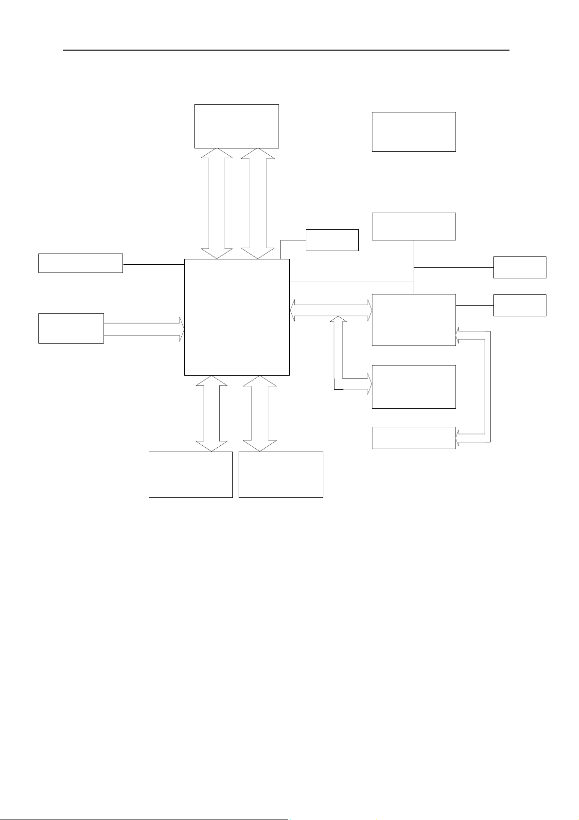
Block Diagram
J1 Top Pri mary TIM
JTAG Header
Connector
Comm-Port 0 & 3
26 I/O pins
2x Comm-Ports/SDL
Linear regulat ors
1.5V & 1.2V
15 I/O pins
Timer,& Control
4 LEDs &
4 I/ O pins
McBSP0
McBSP/Ut opia/
GPI O
4 LEDs
Sundance Digi tal Bus
40- way ODU x2
46 I/ O Pins; 16-bit Data
J3 Global Expansi on
FPGA Controller
Connector
Vir tex-II, FG456
324 I/ O Pins
1.5V
74 I/O pins
Global Bus
52 I/O pins
2x Comm-Port/SDL
J2 Bott om Primary TIM
Connector
Comm-Port 1 & 4
92 pins
'C64xx
DSP
525 pins
32 M by tes SDRAM ( EMI FA)
4 x K4S641632 (4M x 16)
Flash ( EMIFB CE1)
Start-up mode sel ecti on.
Oscil lator s
Page 8

Version 2.7 Page 8 of 23 SMT361 SMT361A User Manual
Architecture Description
The SMT361 TIM consists of a Texas Instruments TMS320C64xx running at up to
600MHz whereas the SMT361A TIM consists of a Texas Instruments TMS320C64xx
running at up to 720MHz. Modules are populated with 32MBytes of synchronous
DRAM (SDRAM) which runs at 100 MHz for the SMT361 and 120MHz for the
SMT361A.
A Field Programmable Gate Array (FPGA) is used to manage global bus accesses
and implement four communication ports and two Sundance Digital Buses.
Page 9

Version 2.7 Page 9 of 23 SMT361 SMT361A User Manual
TMS320C64xx
The processor will run with zero wait states from internal SRAM.
An on-board crystal oscillator provides the clock used for the DSP which then
multiplies this by 12 internally.
The TIM configuration feature is fully implemented. This provides a single opencollector line that can be held low until software configuration has been completed.
Boot Mode
The SMT361 is configured to use the following boot sequence each time it is taken
out of reset:
1. The processor copies a bootstrap program from the first part of the flash
memory into internal program RAM starting at address 0.
2. Execution starts at address 0.
The standard bootstrap supplied with the SMT361 then performs the following
operations:
1. All relevant DSP internal registers are set to default values;
2. The FPGA is configured from data held in flash memory and sets up the
communication ports, the global bus and the Sundance Digital Buses. This
step must have been completed before data can be sent to the ComPort from
external sources such as the host or other TIMs;
3. A C4x-style boot loader is executed. This will continually examine the four
communication ports until data appears on one of them. The bootstrap will
then load a program in boot format from that port; the loader will not read data
arriving on other ports. See “Application Development” for details of the boot
loader format;
4. Finally, control is passed to the loaded program.
The delay between the release of the board reset and the FPGA configuration is
around 1s for a SMT361 (400MHz clock).
A typical time to wait after releasing the board reset should be in excess of this delay,
but no damage will result if any of the I/Os are used before they are fully configured.
In fact, the ComPort will just produce a not ready signal when data is attempted to be
transferred during this time.
Page 10

Version 2.7 Page 10 of 23 SMT361 SMT361A User Manual
EMIF Control Registers
The C64xx has two external memory interfaces (EMIFs). One of these is 64 bits
wide, the other 8 bits.
The DSP contains several registers that control the external memory interfaces
(EMIFs). A full description of these registers can be found in the C6x Peripherals
Reference Guide[1].
The standard bootstrap will initialise these registers to use the following resources:
Memory space
(EMIFA)
Internal program memory
Resource Address range
0x00000000 - 0x000FFFFF
(1Mbyte)
CE0 SDRAM 0x80000000 - 0x81FFFFFF
CE1 Virtex 0x90000000 - 0x91FFFFFF
Memory space
(EMIFB)
Resource Address range
CE1 2Mbyte flash (1st half) 0x64000000 – 0x640FFFFF
CE2 2Mbyte flash (2nd half) 0x68000000 – 0x680FFFFF
SDRAM
Memory space CE0 is used to access 32MB of SDRAM over EMIFA. The SDRAM
operates at EMIF clock speed. It is typically 100MHz for the SMT361 and 120MHz for
the SMT361A.
FLASH
A 2MByte Flash ROM device is connected to the DSP EMIFB.
The ROM holds boot code for the DSP, configuration data for the FPGA, and optional
user-defined code.
A software protection algorithm is in place to prevent programs accidentally altering
the ROM’s contents. Please contact Sundance for further information about reprogramming this device via the support forum.
Page 11

Version 2.7 Page 11 of 23 SMT361 SMT361A User Manual
Version control
Revision numbers for both the boot code and FPGA firmware are stored in the Flash
ROM during programming as zero-terminated ASCII strings.
The SMT6001 utility is to be used to know the version of the boot code and the
FPGA.
Reprogramming the firmware and boot code
The reprogramming is made using the SMT6001 utility. It comes with the latest
firmware and boot code for the module and with a complete documentation on how to
reprogram a module. It requires only the correct set-up for code composer (see code
composer section).
To confirm that the programming has been successful you should use the Sundance
Server to reset the board and execute the confidence test using SMTBoardInfo.
Interrupts
See general firmware description
Communication ports
The SMT361 provides 4 ComPorts. They are ComPorts 0, 1, 3 and 4.
ComPorts 2 and 5 are interconnected on the module to allow a bypass to the next
module.
See general firmware description
Page 12

Version 2.7 Page 12 of 23 SMT361 SMT361A User Manual
SDB
The SMT361 provides two Sundance Digital Buses(SDB).
They are numbered SDB0 for SDBA and SDB1 for SDBB .
See general firmware description
SDB Clock selection
At any time you can change the speed of an SDB clock by altering SDBCLK.
Module SDBCLK Clock Speed
SMT361
0 50MHz
1 100MHz
0 60MHz
SMT361A
1 120MHz
Global bus
The SMT361 provides one global bus interface.
See general firmware description
Page 13

Version 2.7 Page 13 of 23 SMT361 SMT361A User Manual
LED Setting
The SMT361 has 9 LEDs.
LED D6 always displays the state of the FPGA DONE pin. This LED is off when the
FPGA is configured (DONE=1) and on when it is not configured (DONE=0).
This LED should go on when the board is first powered up and go off when the FPGA
has been successfully programmed. If the LED does not light at power-on, check that
you have the mounting pillars and screws fitted properly. If it stays on, the DSP is not
booting correctly.
Four of the remaining LEDs can be controlled with the LED register. Writing 1 will
illuminate the LED; writing 0 will turn it off.
LED Register
31–4 3 2 1 0
LED D10 LED D9 LED D8 LED D7
RW,0 RW,0 RW,0 RW,0
The four remaining LEDs (D2-5) are connected to the DSP’s GPIO pins 12-15.
CONFIG & NMI
See general firmware description
Timer
See general firmware description
IIOF interrupt
The firmware can generate pulses on the external interrupt lines of the TIM.
See general firmware description
Page 14

Version 2.7 Page 14 of 23 SMT361 SMT361A User Manual
Code Composer
This module is fully compatible with the Code Composer Studio (CCS) debug
environment. This extends to both the software and JTAG debugging hardware. You
will require updating to version 2.2 or later.
The name of the C64xx CCS device driver is tixds6400.dvr for silicon revision 1.01
and tixds6400_11.dvr for silicon revision 1.1, and should be obtained from Texas
Instruments. In case of difficulty please log onto Sundance’s support forum
http://support.sundance.com/
WARNING:
From the silicon errata sprz011g.pdf
from Texas Instrument:
Revision(s) Affected: 1.03 and earlier
Details: The JTAG port does not work properly if non-C64x devices are in the scan
chain with the C64x device.
Workaround: Place all C64x devices in a separate scan chain.
FIRST TIME DOWNLOAD
When you open CCS and want to download an application, after power up, you might
get the following error message:
“Can’t set breakpoint: Cannot set/verify breakpoint at 0x8C40” (the address might be
different)
Workaround: Reset the board first with a server or you should infer a CPU Reset
from Debug\reset CPU. Then you should run the processor.
You can then stop the processor and load your application
Page 15

Version 2.7 Page 15 of 23 SMT361 SMT361A User Manual
Application Development
You can develop code for SMT361 modules in several ways. The simplest is to use
the Sundance SMT6000 Server Loader and its associated libraries.
The Server Loader is an application that runs on a host PC under either Windows 98
or NT and allows you to run COFF-format applications. Modified forms of the TI RTS
library support standard C I/O.
The Server Loader will read a .out file and convert it into C4x-style boot code which
is then transmitted down a ComPorts to the SMT361.
The boot code is in the following format:
1
Word
1 0 reserved
6-word
header
Words 2, 3, 4 0, 0, 0
Word 5 start address
Word 6 0
Word 1 4*N: Length of load block (in bytes)2
Load Block
Word 2 Destination address (external memory only)
Next N words N data words
0 or more
Load Blocks
Terminator Word 1 03
1
A word is 32 bits
2
The length of each data block will be rounded up to a multiple of 4 bytes if necessary.
3
Effectively a zero-length Load Block
Page 16

Version 2.7 Page 16 of 23 SMT361 SMT361A User Manual
Operating Conditions
Safety
The module presents no hazard to the user.
EMC
The module is designed to operate within an enclosed host system that provides
adequate EMC shielding. Operation within the EU EMC guidelines is only guaranteed
when the module is installed within an appropriate host system.
The module is protected from damage by fast voltage transients introduced along
output cables from outside the host system.
Short-circuiting any output to ground does not cause the host PC system to lock up
or reboot.
General Requirements
The module must be fixed to a TIM40-compliant carrier board.
The SMT361 TIM is in a range of modules that must be supplied with a 3.3v power
source. In addition to the 5v supply specified in the TIM specification, these new
generation modules require an additional 3.3v supply to be presented on the two
diagonally-opposite TIM mounting holes. The lack of this 3.3v power supply should
not damage the module, although it will obviously be inoperable; prolonged operation
under these circumstances is not recommended.
This module is not directly compatible with earlier generations of TIM motherboards,
although the 3.3v supply can be provided from a separate source. It is, however,
compatible with the latest generation of Sundance TIM carrier boards such as the
SMT320V4 and subsequent versions (PCI), and SMT328 (VME), which present the
3.3v via conductive mounting pillars.
Use of the TIM on SMT327 (cPCI) motherboards may require a firmware upgrade. If
LED D6 on the SMT361 remains illuminated once the TIM is plugged in and powered
up, the SMT327 needs the upgrade. The latest firmware is supplied with all new
boards shipped. Please contact Sundance directly if you have an older board and
need the upgrade.
A SMT320V3 motherboard can be used providing a SMT361 TIM is not located in the
first slot; putting one there prevents the SMT320V3 from coming out of reset. Any
other type of TIM must be placed in the first slot of this motherboard to ensure correct
operation.
The external ambient temperature must remain between 0°C and 40°C, and the
relative humidity must not exceed 95% (non-condensing).
Page 17

Version 2.7 Page 17 of 23 SMT361 SMT361A User Manual
Power Consumption
The power consumption of this TIM is dependent on the operating conditions in terms
of core activity and I/O activity. The maximum power consumption is 3W.
Connector Positions
Page 18

Version 2.7 Page 18 of 23 SMT361 SMT361A User Manual
Serial Ports & Other DSP I/O
The C64 contains various I/O ports. These signals are connected to a 0.1” pitch DIL
pin header. The pin-out of this connector is shown here:
P O DR0 FSR0 DX0 FSX0 CLKR0 CLKX0 CLKS0 CLKS1
URA3
L A DR2 FSR2 DX2 FSX2 CLKR2 CLKX2 CLKS2
GPIO8
R I URD0 URD1 URD2 URD3 URD4 URD5 URD6 URD7 URCLK URENB URCLAV URSOC
S A UXD0 UXD1 UXD2 UXD3 UXD4 UXD5 UXD6 UXD7 UXCLK UXENB UXCLAV UXSOC
DX1
UXA4
CLKX1
URA4
FSX1
UXA3
CLKR1
URA2
FSR1
UXA2
URA1 URA0
DR1
UXA1
UXA0
T I NC
O N GPIO0 GPIO1 GPIO2 GPIO3 GPIO4 GPIO5 GPIO6 GPIO7 GND GND TTL0 TTL1
GPIO9 GPIO10 GPIO11 GPIO12 GPIO13 GPIO14 GPIO15 V33 V33 TTL2 TTL3
FPGA and CPLD JTAG
The following shows the pin-outs for JP2 (CPLD) and JP5 (FPGA) JTAG connectors:
Signal Pin Pin Signal
V33 1 2 TCK
GND 3 4 TMS
TDO 5 6 TDI
Page 19

Version 2.7 Page 19 of 23 SMT361 SMT361A User Manual
Virtex Memory Map
See general firmware description with i = 14
The memory mapping is as follows:
#define CP0 (volatile unsigned int *)0x90000000
#define CP1 (volatile unsigned int *)0x90008000
#define CP2 (volatile unsigned int *)0x90010000
#define CP3 (volatile unsigned int *)0x90018000
#define CP4 (volatile unsigned int *)0x90020000
#define CP5 (volatile unsigned int *)0x90028000
#define CP0_STAT (volatile unsigned int *)0x90004000
#define CP1_STAT (volatile unsigned int *)0x9000C000
#define CP2_STAT (volatile unsigned int *)0x90014000
#define CP3_STAT (volatile unsigned int *)0x9001C000
#define CP4_STAT (volatile unsigned int *)0x90024000
#define CP5_STAT (volatile unsigned int *)0x9002C000
#define GBSTAT (volatile unsigned int *)0x90034000
#define SDBSTAT (volatile unsigned int *)0x90038000
#define STAT (volatile unsigned int *)0x9003C000
#define SDBA (volatile unsigned int *)0x90040000
#define SDBB (volatile unsigned int *)0x90050000
#define SDBA_STAT (volatile unsigned int *)0x90048000
#define SDBB_STAT (volatile unsigned int *)0x90058000
#define SDBA_INPUTFLAG (volatile unsigned int *)0x90044000
#define SDBB_ INPUTFLAG (volatile unsigned int *)0x90054000
#define SDBA_OUTPUTFLAG (volatile unsigned int *)0x9004C000
#define SDBB_OUTPUTFLAG (volatile unsigned int *)0x9005C000
#define GLOBAL_BUS (volatile unsigned int *)0x900A0000
#define GLOBAL_BUS_CTRL (volatile unsigned int *)0x90080000
#define GLOBAL_BUS_START (volatile unsigned int *)0x90088000
#define GLOBAL_BUS_LENGTH (volatile unsigned int *)0x90090000
#define TCLK (volatile unsigned int *)0x900C0000
#define TIMCONFIG (volatile unsigned int *)0x900C8000
#define LED (volatile unsigned int *)0x900D0000
#define IIOF (volatile unsigned int *)0x900D8000
#define INTCTRL4 (volatile unsigned int *)0x900E0000
#define SDBINTCTRL4 (volatile unsigned int *)0x900E4000
#define INTCTRL5 (volatile unsigned int *)0x900E8000
Page 20

Version 2.7 Page 20 of 23 SMT361 SMT361A User Manual
#define SDBINTCTRL5 (volatile unsigned int *)0x900EC000
#define INTCTRL6 (volatile unsigned int *)0x900F0000
#define SDBINTCTRL6 (volatile unsigned int *)0x900F4000
#define INTCTRL7 (volatile unsigned int *)0x900F8000
#define SDBINTCTRL7 (volatile unsigned int *)0x900FC000
Page 21

Version 2.7 Page 21 of 23 SMT361 SMT361A User Manual
SDB Pin-Out
Pin Signal Signal Pin
1 CLK GND 2
3 D0 GND 4
5 D1 GND 6
7 D2 GND 8
9 D3 GND 10
11 D4 GND 12
13 D5 GND 14
15 D6 GND 16
17 D7 GND 18
19 D8 GND 20
21 D9 GND 22
23 D10 GND 24
25 D11 GND 26
27 D12 GND 28
29 D13 GND 30
31 D14 GND 32
33 D15 GND 34
35 UD0 DIR 36
37 WEN REQ 38
39 UD1 ACK 40
Page 22

Version 2.7 Page 22 of 23 SMT361 SMT361A User Manual
Bibliography
1. TMS320C64xx Peripherals Reference Guide (literature number SPRU190)
http://www-s.ti.com/sc/psheets/spru190e/spru190e.pdf
Describes common peripherals available on the TMS320C64xx digital signal processors. This
book includes information on the internal data and program memories, the external memory
interface (EMIF), the host port, multichannel-buffered serial ports, direct memory access (EDMA),
clocking and phase-locked loop (PLL), and the power-down modes.
2. SMT6001 http://www.sundance.com/edge/files/productpage.asp?STRfilter=smt6001
3. TIM-40 MODULE SPECIFICATION Including TMS320C44 Addendum
ftp://ftp2.sundance.com/Pub/documentation/pdf-files/tim_spec_v1.01.pdf
4. SDB Technical Specification
http://www.sundance.com/edge/files/productpage.asp?STRfilter=sdb
5. SHB Technical Specification
http://www.sundance.com/edge/files/productpage.asp?STRfilter=shb
6. TMS320C4x User's Guide (literature number SPRU063)
http://www-s.ti.com/sc/psheets/spru063c/spru063c.pdf
Describes the C4x 32-bit floating-point processor, developed for digital signal processing as well
as parallel processing applications. Covered are its architecture, internal register structure,
instruction set, pipeline, specifications, and operation of its six DMA channels and six
communication ports. Software and hardware applications are included.
7. Xilinx Virtex-II data sheet:
http://www.xilinx.com/xlnx/xil_prodcat_landingpage.jsp?title=Platform+FPGAs
8. Texas Instruments TMS320C6416 data sheet:
http://www-s.ti.com/sc/ds/tms320c6416.pdf
Page 23

Version 2.7 Page 23 of 23 SMT361 SMT361A User Manual
Index
Application Development...............15
server-loader.................................15
Architecture Description..................8
Bibliography....................................22
Block Diagram ..................................7
Board not working
firmware revision.............................2
LED 6 illuminated..........................13
no 3.3v supply...............................16
boot code format ............................15
Boot Mode.........................................9
bootstrap program ...........................9
carrier boards .................................16
Code Composer..............................14
config line..........................................9
Contacting Sundance.......................4
EMIF Control Registers..................10
field values after reset......................5
Flash ................................................10
protection algorithm ......................10
FPGA .................................................8
configuration ...................................9
LEDs ................................................13
FPGA DONE pin ...........................13
LED register ................................. 13
memory space (CE0 to CE3)......... 10
motherboards................................. 16
NMI .................................................. 13
Notational Conventions .................. 5
Operating Conditions .................... 16
Power
3.3v .............................................. 16
power consumption ...................... 17
register descriptions ....................... 5
revision numbers
boot code ..................................... 11
FPGA firmware............................. 11
SDB ................................................. 12
clock speed .................................. 12
pin-out .......................................... 21
SDRAM ........................................... 10
Serial Ports..................................... 18
SMT361 ............................................. 5
Sundance TIM carrier boards ....... 16
Timer............................................... 13
TMS320C64xx................................... 9
Virtex
memory map ................................ 19
 Loading...