

Page 1

User Manual
User Manual (QCF42); Version 3.0, 8/11/00; © Sundance Multiprocessor Technology Ltd. 1999
Page 2

Version 2.5 Page 2 of 25 SMT358 User Manual
Revision History
Date Comments Engineer Version
10 Feb
1999
20 Sept
Overall update to SMT358 User Manual E.Puillet Version1.1
1999
12 Oct
1999
08 Nov
1999
22 Nov
1999
08 Dec
1999
07 Jan
2000
28 Jan
2000
15 Feb
2000
SDB connector Pins renamed.
Addition of Global Clock Buffer signal assignments
Modification of the FSM for the FPGA
Reconfiguration.
Addition of TIM Connectors and mounting
holes’ position
Clarification of the FSM and explanations for
the FPGA Configuration and Reconfiguration.
SDB bi-directional clock drawing in Figure 4
corrected
SDB Connector Pins correspondence between
SMT373 and SDB standard.
Description of the Installation and configuration
of the SMT358
Initial Release
E.Puillet Version1.0
E.Puillet Version1.2
E.Puillet Version
1.3
E.Puillet Version
1.4
E.Puillet Version
1.5
E.Puillet Version
1.6
E.Puillet Version
1.7
E.Puillet Version
1.8
07 March
2000
22 March
2000
20 July
2000
26
October
2000
06
January
2001
23
January
2001
Addition of a WARNING for customers with
SMT358 boards delivered before 07.03.00.
Addition of the memory addressing scheme
for a memory Bank.
Figure 3 modification of SDB bi-directional
signal number for SDB C and D
Table 3 is modified and becomes Table
1.General modifications to adapt the User
Manual to VirtexE
Table 1 is modified to remove parts, which
won’t be fitted on SMT358. Addition of new
conversion software.
Addition of power consumption considerations
for the SMT358
E.Puillet Version
2.0
E.Puillet Version
2.1
E.Puillet Version
2.2
E.Puillet Version
2.3
E.Puillet Version
2.4
E.Puillet Version
2.5
Page 3

Version 2.5 Page 3 of 25 SMT358 User Manual
The FPGARESET signal must be tied to ground in any FPGA design
for SMT358s received before 07.03.00.
SMT358s received after 07.03.00 see the FPGA constraint file
modified for Comm-Port 3 and any FPGA design must use the
FPGARESET signal as a global reset active low.
Page 4

Version 2.5 Page 4 of 25 SMT358 User Manual
Table of Contents
Revision History..........................................................................................................2
Table of Contents........................................................................................................4
Scope..........................................................................................................................6
SMT358 Versions....................................................................................................... 6
SMT358 Power consumption Considerations............................................................. 7
Technical description..................................................................................................8
On-board SRAM......................................................................................................9
Sundance Digital Bus (SDB).................................................................................11
SMT358-DSP Communication channels............................................................... 12
Sundance Datapipe Links..................................................................................... 13
FPGA ....................................................................................................................14
Global Clock Buffers..............................................................................................15
Installation.................................................................................................................16
Configuration ............................................................................................................16
Hardware Sequence of events..............................................................................16
At power-up....................................................................................................... 16
FPGA Reconfiguration..........................................................................................18
Once configured................................................................................................18
FPGA Reconfiguration in real time........................................................................ 18
Software tools ....................................................................................................... 19
The Bit to Dat Conversion..................................................................................20
The Dat to Obj conversion................................................................................. 20
Interface.................................................................................................................... 21
TIM Connectors’ Position..........................................................................................22
Page 5

Version 2.5 Page 5 of 25 SMT358 User Manual
LIST OF FIGURES
FIGURE 1: SMT358 BLOCK DIAGRAM.............................................................................................................8
FIGURE 2: ZBT SRAM CLOCK SIGNAL............................................................................................................9
FIGURE 3: FPGA, MEMORY AND SDB COMMUNICATION CHANNELS .................................................10
FIGURE 4: MEMORY ADDRESSING ............................................................................................................... 11
FIGURE 5: FPGA-DSP COMMUNICATION CHANNELS...............................................................................13
FIGURE 6: GLOBAL CLOCK BUFFERS ASSIGNMENTS IN THE VIRTEX/E.............................................15
FIGURE 7: GLOBAL RESET ROUTING. USE OF FPGARESET AS A GLOBAL RESET FOR DESIGNS.. 17
FIGURE 8: FPGA RECONFIGURATION...........................................................................................................18
FIGURE 9: SMT358 LAYOUT............................................................................................................................21
FIGURE 10: TIM CONNECTORS’ POSITION..................................................................................................22
FIGURE 11: TIM DIMENSIONS AND MOUNTING HOLES POSITIONS .....................................................23
LIST OF TABLES
TABLE 1: VIRTEX/E-ZBT SRAM COMBINATIONS........................................................................................6
TABLE 2: SMT358 CONNECTOR REFERENCE TABLE................................................................................22
TABLE 3: 40 WAY SDB CONNECTOR PINS...................................................................................................24
TABLE 4: JTAG CONNECTOR..........................................................................................................................25
Page 6
Version 2.5 Page 6 of 25 SMT358 User Manual
Scope
This document describes the architecture, the function, the use and the interface
considerations for the SMT358. This document is intended for both the users of the SMT358
and the designer who is interested in designing the FPGA provided on the Board.
SMT358 Versions
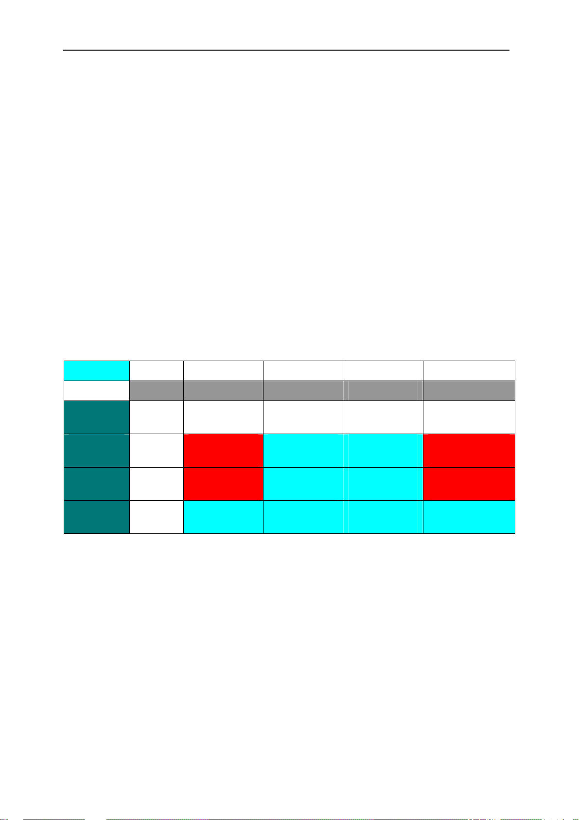
The SMT358 comes under 4 standard versions, highlighted in red in Table 1. A Virtex
or Virtex E is fitted and the ZBTSRAM is in the pipelined version.
The total amount of memory on the board is either 4 MBytes or 8 Mbytes or 16
Mbyte.
Depending on the amount of on-board memory required, the Virtex/E fitted on-board,
the SMT358 can be implemented in 18 subversions, which can be adapted to a wide
range of application needs and costs.
Other configurations are possible depending on the speed of the application, as
shown in Table 2 and Table 3.
Table 1 summarises the various board configurations offered.
SMT358
Virtex/E XCV400 XCV600 XCV800 XCV1000E
ZBT
SRAM
4MBytes SMT358-
400-4
8 MBytes SMT358-
400-8
16
MBytes
SMT358-
400-16
SMT358-
600-4
SMT358-
600-8
SMT358-
600-16
SMT358-
800-4
SMT358-
800-8
SMT358-
800-16
SMT358-
1000E-4
SMT358-
1000E-8
SMT358-
1000E-16
Table 1: Virtex/E-ZBT SRAM Combinations
Page 7

Version 2.5 Page 7 of 25 SMT358 User Manual
SMT358 Power consumption Considerations
The SMT358 power consumption is mostly dependant on the Virtex fitted and its
usage.
When using a S MT3581000E, suff icient cooling is provid ed on-board for t he voltage
regulator and for the Virtex 1000E, nevertheless a correct airflow MUST prevail in
your PC.
The larger and the faster the Virtex FPGA design is, the higher the Virtex power
consumption is.
For example, considering a shift register using 50% of the LUTs of a Virtex 1000E at
100 Mhz with data toggling at every clock cycle will have the effect of drawing more
current than the voltage regulator can provide and will make the voltage regulator fail
(safely) and the FPGA will loose its configuration.
Therefore, we advice customers to use Xilin x power estimator to determine the worstcase power consumption of their design AND to consult.
The Excel program can be found at:
http://support.xilinx.com/support/techsup/powerest/virtex_power_estimator_v15.xls
The user guide on how to use this program can be found at:
http://support.xilinx.com/xapp/xapp152.pdf
Page 8
Version 2.5 Page 8 of 25 SMT358 User Manual
Technical description
ZBT SRAM
ZBT SRAM
ZBT SRAM
ZBT SRAM
BANK1
40 way IDC
SDB_ConA
40 way IDC
SDB_ConB
40 way IDC
SDB_ConC
SDB A
SDB B
SDB C
BANK2
Memory Signals
XCVxxxxxBG560
FPGA
BANK3
Memory Signals
Com-Port 1,4
Control
D[31:0]
A[30:0]
BANK4
Bottom Primary
Connector
Global Bus
Connector
40 way IDC
SDB_ConD
SDB D
50MHz Oscillator
Config Control
Com-Port 3 Ctrl Com-Port 3 Data
Figure 1: SMT358 Block diagram
Config D[7:0]
Configuration Logic CPLD
IIOF2
H1
Com-Port 0
Top Primary
Connector
Com-Port 3
Page 9

Version 2.5 Page 9 of 25 SMT358 User Manual
A
Figure 1 shows the block diagram of the SMT358 I/O module. The following section
describes the SMT358 from a user’s point of view. Reference is made to the different blocks
of Figure 1 in the next Figures.
On-board SRAM
The SMT358 provides the user with pipelined or Flowthrough ZBT (Zero Bus Turnaround)
SRAM from Micron. Therefore this type of SRAM is optimised for a 100 percent bus
utilisation eliminating any cycle when transitioning from READ to WRITE or vice versa.
Three Chip Enables allow easy depth expansion so that the SMT358 total amount of memor y
can vary from 4 MBytes up to 16 MBytes.
Micron 4,8 or 16 Mbit ZBTSRAM have compatible inputs and outputs. FPGA designers can
find the general description and a Pin description in the latest data sheets on Micron’s Web
Site at http://www.micron.com/mti/msp/html/zbtds.html
The on-board memory is divided into four banks (bank 1 to 4) accessible on a 72-bit bus (4
18-bit busses) and can be run at frequencies up to 166Mhz and.
Each of the 4 SRAM banks is independently accessible (Control, Data and Address are
independent for every bank) and share the s ame Clock signal. To ensure high performance,
the clock signal can be de-skewed inside the FPGA using DLLs as reproduced in Figure 2. As
a result, a high-speed de-skewed clock drives the controller inside the FPGA and the ZBT
SRAM.
The Virtex provides four programmable DLLs to produce waveforms with a wide range of
frequencies and duty cycles.
BoardClk
DLL
CONTROLLER
Clk2x
ddr
RNW
Data
ZBT SRAM BANK1, 2,3,4
DLL
VIRTEX/E
Clk2x
SMT358
Figure 2: ZBT SRAM Clock signal
Page 10

Version 2.5 Page 10 of 25 SMT358 User Manual
A simple Virtex/E interface to ZBTSRAM is provided by Xilinx and is described in Xilinx’s
Application Note: xapp136.
The on-board SRAM can be extended of another 8Mword bank present on a Mez zanine card
which connects on two of the four SMT358 SDB connectors shown in Figure 3.
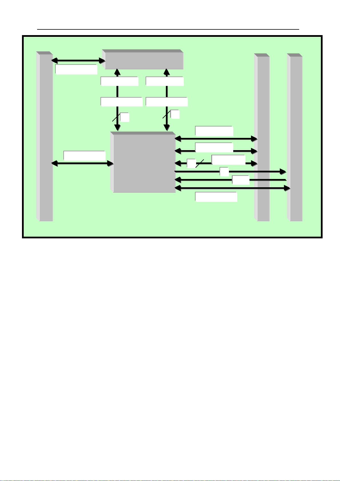
Figure 3 is a detailed view of the memory signal connections to the FPGA.
ZBT SRAM
BANK1
ZBT SRAM
BANK2
21 21
1818
6 6
40 way IDC
SDB_ConA
40 way IDC
SDB_ConB
Add LinesAdd Lines
Data lines Data lines
Control Control
SDB A 23
Clk A
FPGA
XCVxxxxx
SDB B 23
Clk B
Data lines Data lines
18 18
21 21
ZBT SRAM
BG560
Control Control
66
ZBT SRAM
Add LinesAdd Lines
SDB C 22
Clk C
SDB D 22
Clk D
40 way IDC
SDB_ConC
40 way IDC
SDB_ConD
BANK3
BANK4
Figure 3: FPGA, Memory and SDB Communication Channels
Page 11

Version 2.5 Page 11 of 25 SMT358 User Manual
A
]
A
]
A
]
A
]
As shown in Figure 4 each ZBTSRAM Bank is composed of a Low Bank and a High
Bank which are selected by Address[20].
• Addr[20] = 0 selects the Low bank
• Addr[20] = 1 selects the High bank
CONTROLLER
VIRTEX/E
Figure 4: Memory Addressing
ddr[20
ddr[19:0
CE2
#CE2
ddr[19:0
ddr[19:0
SMT35
ZBT SRAM High BANK1, 2,3,4
ZBT SRAM Low BANK1, 2,3,4
Sundance Digital Bus (SDB)
The four 40-way miniature IDC connectors’ primar y function is to provide bi-directional 16bit data paths between TIMs with data transfer rates over 200 MBytes/s.
Data rates of 200 MBytes/second through a connector have been achieved using a
ground interlaced signal cable.
Each high speed Sundance Digital Bus (SDB) Interface can transfer 16-bit data, to
and from the TIM, at such a transfer rate.
400 MBytes/Second Data rates can be reached using in parallel 2 (SDB) Interfaces
to send a 32-bit data every clock cycle at 100 MHz
The SDB Interface packs the 16-bit data transmitted into a 32-bit Word and stacks
them into a FIFO ready to be used.
The transmission can be fully bi-directional.
Many of Sundance TIM modules are being designed with this interface.
A SDB Interface is available from Sundance Multiprocessor Technology IP Centre.
Page 12

Version 2.5 Page 12 of 25 SMT358 User Manual
Alternatively, the Sundance Digital Bus links can be extended to external
interconnection by connecting them to the SMT373 mez zanine card.
With this card, TTL signals are converted to Low-Voltage Differential signals and can
connect two systems several meters apart.
It provides two bi-directional 20-bit channels that can transfer up to 2 Gbytes/s through fort y
SN65LVDM176 transceivers. Each channel provides 16 bit of data, a clock and a clockenable signal with their direction controlled by one signal. Two other signals can be used for
the bus arbitration in a bi-directional application. The direction of each of them can be
controlled independently.
All the signals controlling the direction are connected to the SMT358 FPGA through the
connectors and so can be controlled by software.
SMT358-DSP Communication channels
The global bus or Comm-Port 0,1,3 or 4 are communication channels of the SMT358 used to
interfaced to T.I.’s DSP processors.
The ‘C4x Protocol defines Byte-wide links which can theoretically transmit at
20MBytes/second asynchronously between TIMs.
The Global Bus is only available when the SMT358 is connected onto the SMT350PB mother
board.
The SMT350PB provides a non-blocking global bus interconnection between any source TIM
site and any other destination TIM site. It provides a sustainable throughput of 50 MBytes/s
between any of the module sites even with three modules accessing the same destination
module. Access to the PCI bus takes place through T IM site 1. Please see our Web Site at
http://www.sundance.com/
Figure 5 shows the various dedicated DSP communication channels available on the SMT358
for inter-TIM data transfers.
Page 13
Version 2.5 Page 13 of 25 SMT358 User Manual
Top Primary Connector
Com-Port 3
Com-Port 0
Configuration Logic CPLD
Config Control
Com-Port 3 Ctrl Com-Port 3 Data
4
Config D[7:0]
8
FPGA
XCVxxxx
BG560
Global A[30:0]
Global D[31:0]
10
Com-Port 1,4
Bottom Primary Connector
Global Bus Connector
Global CTRL
H1
IIOF2
Figure 5: FPGA-DSP Communication Channels
For developers who want to interface a SMT358 to a C4x or C6x TIM like the SMT302,
SMT331 or SMT332 via Comm-Ports or the Global Bus, a Comm-Port interface and a Global
Bus interface are available from Sundance Multiprocessor Technology IP Centre.
Sundance Datapipe Links
The Comm-Port connections provided on the SMT358 can be used as Sundance Datapipe
Links for fast data transfers between SMT338V2-SMT358 or ‘C6x TIM based boards like the
SMT335.
An SDB interface is used and offers up to 100 MHz on copper and 50 MHz on flat-ribbon
cables like the FMS used on the Sundance range of carrier boards.
Page 14

Version 2.5 Page 14 of 25 SMT358 User Manual
FPGA
The FPGA is to be configured over Comm-Port 3 via the CPLD. The configuration bitstream
is sent by a host, a ‘C6x or ‘C4x processor. This feature will allow a system to dynamically
change the FPGA firmware. The configuration LED indicates that configuration is complete.
The FPGA drives 4 LEDs, and is connected to it’s own local oscillator package.
The FPGA firmware will be user defined, and can be done on demand.
Typical functions that can be implemented in the FPGA are:
• Full bi-directional global-bus interface
• Full bi-directional Comm-Port interface
• Bi-directional SDB Interface
• RAM, FIFOs, Dual port RAMs up to a total of 16K Bytes
• Communication protocols
• DSP pre-processors
• Any digital function that will fit in this size device
The SMT358 TIM can typically be used to interface with a SMT338 Frame Grabber over the
SDB connectors. The SMT358 can then perform customer specific data formatting before
sending it to a nearby DSP TIM via Comm-Port or SDB.
Due to the parallel nature of an FPGA it is well suited to handle multiple high-speed I/O lines.
The FPGA can then provide a cleaner bus-interface to the associated DSP processors.
Page 15

Version 2.5 Page 15 of 25 SMT358 User Manual
Global Clock Buffers
The Virtex/E provides four independent Global C lock Buffers, which allow the use of 4 or 8
(for a Virtex E) programmable DLLs to produce waveforms with a wide range of f requencies
and duty cycles.
Figure 6 shows the signals assignment to each Global Clock Buffer.
40 way IDC
SDB_ConA
40 way IDC
SDB_ConB
BANK0
FPGA
BANK1
XCVxxxx
BG560
BANK4 BANK5
ZBT SRAM BANK1, 2,3,4
Figure 6: Global Clock Buffers assignments in the Virtex/E
Page 16

Version 2.5 Page 16 of 25 SMT358 User Manual
Installation
The minimum system requirements needed to run a SMT358 on a PC is a C4x TIMbased carrier board and a C4x or C6x TIM with at least a Transmit Comm-Port
(Comm-Port 0,1 or 2) at Reset.
The goal is to connect one of the processors Comm-Port to Comm-Port 3 of the
SMT358.
Follow these steps to install the SMT358 module on a Host system:
1. Remove the carrier board from the host system.
2. Place the SMT358 module into one of the TIM sites on the carrier board.
3. Make sure the that the board is firmly seated, then provide the 3.3V to the board
by screwing the SMT358 on the two main mounting holes with the bolts and
screws provided with the board.
4. Fit the processor-based board on the carrier board. To do so, please follow the
installation procedure of that specific board. In the case of a SMT320 carrier
board, the C4x or C6x board MUST be placed on the first TIM slot (TIM slot 0) of
the SMT320.
5. Connect at least Comm-Port 3 of the SMT358 to one of the transmit Comm-Port
(at Reset) available on the Processor-based board.
6. Connect the SDB links as well if required by your application.
7. Replace the carrier board in the host system.
Configuration
The FPGA configuration is done by a software routine running on a host, ‘C6x or
‘C4x processor that downloads a bitstream to the Virtex/E via the CPLD using
Comm-Port 3(on the SMT358). After configuration, the CPLD gives the hand to the
FPGA, which becomes the owner of Comm-Port 3.
The CPLD does the handshake with the Comm-Port and communicates with the
FPGA as well.
The following description is referring to Figure 7.
Hardware Sequence of events
At power-up.
1) The CPLD polls Comm-Port 3 until it receives the keyword 0xBCBCBCBC.
(WAITFORCMD State)
Page 17

Version 2.5 Page 17 of 25 SMT358 User Manual
2) On receiving the start-of-bitstream keyword 0xBCBCBCBC, The CPLD reads out
the FPGA bitstream from Comm-Port 3 and configures the FPGA (CONFIG
State).
3) The FPGA releases its DONE pin when the configuration phase is finished. At
this time LED1 goes on (LED1 is directly driven by DONE). Then, the FPGA
completes its startup sequence and the design downloaded is now ready to start.
• If the design inside the FPGA in stantiates Comm-Port 3: it must be kept reset
while the bitstream finishes to be downloaded. To do so, use the
FPGARESET pin as a global reset for the Comm-Port interface in particular
and for the whole design in general. FPGARESET is a bi-directional active low
signal. The CPLD asserts FPGARESET low until it receives the end-ofbitstream word BCBCBC00 defining the end of the configuration process and
enters an IDLE State waiting for an interrupt (general TISRESET from the PCI
or FPGARESET coming from the FPGA this time).
• If the design inside the FPGA doesn’t instantiate Comm-Port 3: The CPLD
asserts FPGARESET low until it receives the end-of-bitstream word
0xBCBCBC00 defining the end of the configuration process and enters an
IDLE State waiting for an interrupt (general TISRESET from the PCI or
FPGARESET from the FPGA). Meanwhile, the FPGA design can start if it
doesn’t use FPGARESET as a global reset. (but a good practice is to use
FPGARESET as a global reset).
FPGARESET
FPGARESET
Logic
OR
TIS_RESET
FPGA
XCVxxxxxBG560
Config Control
Com-Port 3 Ctrl Com-Port 3 Data
Configuration Logic CPLD
Config D[7:0]
Top Primary
Connector
TIS_RESET
Com-Port 3
TIS_RESET
Figure 7: Global Reset routing. Use of FPGARESET as a global reset for designs.
Page 18

Version 2.5 Page 18 of 25 SMT358 User Manual
FPGA Reconfiguration
The following description is referring to Figure 8.
Once configured.
When a TISR ESET is received by the SMT358, the CPLD and the FPGA are reset.
4) The CPLD owns Comm-Port 3 and can configure the FPGA with a new bitstream
(repeat step 2).
5) The CPLD can leave Comm-Port 3 available to the FPGA and enter an Idle state
on receiving the command BCBCBC00.
Figure 8: FPGA reconfiguration
FPGA Reconfiguration in real time
The SMT358 can be reprogrammed on-the fly by sending a new bitstream to the
Virtex/E FPGA.
It is possible to reconfigure the Virtex/E dynamically by sending a reconfigure
command to it.
The circuit recognizing a reconfiguration request must be implemented in the FPGA,
so any user-defined command can be sent over a Comm-port for instance.
An example design is provided in the software package for the SMT358 (SMT6358).
Page 19

Version 2.5 Page 19 of 25 SMT358 User Manual
The design makes use of a Comm-port to pass the reconfigure command to the
SMT358 FPGA and waits for a 1 on the LSB of this Comm-Port.
If another Comm-port than Comm-port 3 is used, the pins corresponding to Commport 3 on the FPGA must be tied to “1” in the FPGA (As designed in the
reconfiguration example design)
The following description is referring to Figure 8.
6) The FPGA reads the command and then warns the CPLD by sending an interrupt
(FPGARESET low) that it decoded a reconfigure command. The FPGA goes into
a RESET state and leaves Comm-port 3 available for the CPLD. (in case Commport3 is used by the design).
7) On receiving the FPGARESET interrupt, the CPLD goes into the WAITCMD State
and polls Comm-port 3 for a keyword. (0xBCBCBCBC or 0xBCBCBC00)
8) On receiving the keyword,
• If it is the end-of-bitstream keyword 0xBCBCBC00, the FPGA DOES NOT get
reconfigured, the CPLD leaves Comm-port 3 available for the FPGA and
enters into an IDLE state to wait for the next interrupt.
• If it is the start-of-bitstream keyword 0xBCBCBCBC, repeat step 2 to 3).
Software tools
The SMT6358 is a suite of software support for the SMT358.
It contains:
• A library of IP cores: a Comm-port Interface, an SDB interface and a ZBT
Controller.
• Design examples of Comm-Port, SDB and memory applications.
• The pin allocation file for the Virtex/E: VIRTEX_TOP.ucf.
• 2 conversion softwares needed AFTER a bitstream has been generated to
download it in the SMT358 FPGA.
Some additional software is required:
• A CAD platform to create a schematic or VHDL design.
• A simulator to simulate the hardware designs.
• Xilinx Place & Route software such as M3.3 i.
• Texas Instrument C compiler or 3L parallel C compiler.
Page 20

Version 2.5 Page 20 of 25 SMT358 User Manual
The bitstream that is used to configure the Virtex/E on the SMT358 is built using
Xilinx Design implementation tools for FPGAs such as M2.1i.
Follow these steps to build a bistream that can be executed on the SMT358:
1. Select your design available in edif format (filename.edf) with the Xilin x too ls.
2. Target the constraint file provided with the SMT358 to map your design to the
Virtex/E ’s I/O pins (comment out all the I/Os that your design doesn’t use)
3. Run Xilinx Design imp lementation tools.
4. Next the bitstream is generated (Entityname.bit). The bitstream is a binary image
of the VHDL core.
The Bit to Dat Conversion
5. Format the Entityname.bit to an Entityname.dat file with the standalone
application bit2dat.exe. To do so, you need to modify the Bit2dat.dat file.
• Place the file Entityname.bit in the folder containing the executable file
Bit2dat.exe.
• Edit the file Bit2dat.bat file.
• Replace “bit2dat bitfilename bitfilename ” by “bit2dat Entityname Entityname”.
Note that the extension “.bit” is not necessary.
• Save and double click the bit2dat.bat file. The executable is called and
generates a “.dat” file.
6. At this point the hardware core is ready for implementation in an application.
7. With an application running on the Processor-based board which the SMT358 is
connected to, send the file Entityname.dat through the Comm-port connected to
Comm-Port3 on the SMT358.
The Dat to Obj conversion
Users need to have CCStudio installed, even if they prefer working with 3L as the dat
to obj conversion requires an executable installed under CCStudio. (Asm6x.exe)
The reason for this conversion is that the download over JTAG (using CCStudio) of
the .dat bitstream can take several minutes with CCStudio and around 30 secs using
3L but it will be instantaneous with the method de scribed below.
The “. Dat” needs to be converted in an “. obj” file so that it can be added to the “.out”
application that is run under CCStudio or to the “.app” application that is run under 3L
for configuring the SMT358 FPGA.
Then the download of the bitstream is speeded up because the bitstream is read out
of the on-board memory of the DSP board instead of being read out of the Hard
Drive.
Page 21

Version 2.5 Page 21 of 25 SMT358 User Manual
A
The download is instantaneous if the following method is used:
Format the Entityname.dat to an Entityname.asm file with the standalone
application Dat2asm.exe. To do so, you need to modify the Dat2asm.bat file.
a. Place the file Entityname.dat in the folder containing the executable
file Dat2asm.exe.
b. Edit the file Dat2asm.bat file.
c. Replace “Dat2asm bitfilename.dat bitfilename.asm ” by “Dat2asm
Entityname.dat Entityname.asm”. Note that the extensions “. dat”
and “. Asm” are necessary.
d. Replace “asm6x bitfilename.asm” by “asm6x Entityname.asm”. (The
asm6x executable is included in CCStudio).
e. Save and double click the Dat2asm.bat file. The executable is called
and generates a “. obj” file.
Once the .obj file is generated, it can be linked with the configuration program
(xxx.out for CCStudio or xxx.app for 3L)
Interface
P2
SDB A SDB B
ZBTSRAM
VIRTEX FPGA
ZBTSRAM
Bank2
LED
OSC
Bank1
4 LEDs
Bank0
ZBTSRAM
ZBTSRAM
Bank3
P2
SDB C
Bank0
ZBTSRAM
SDB Conn1 D
J
T
G
ZBTSRAM
Bank3
CPLD
95144
TQ100
Bank1
ZBTSRAM
Voltage
regu
lator
ZBTSRAM
Bank2
P1
P1
Figure 9: SMT358 Layout
Page 22

Version 2.5 Page 22 of 25 SMT358 User Manual
Figure 9 shows the Physical Layout of the SMT358, indicating the external
connectors with their location and numbering.
Connector definitions are as follows:
SDB
: Digital Data & Clock Input /Output Signal – Sundance Digital Bus High
Density ODU connector A (40-way High Density IDC Connectors).
A,B,C,D
JTAG : JTAG Signals – 6-way connector.
P1 : Top Primary connector.
P2 : Bottom Connector. (Bottom Primary and Global Expansion Connectors)
Table 2: SMT358 connector reference table
TIM Connectors’ Position
Figure 10: Tim Connectors’ position
Page 23

Version 2.5 Page 23 of 25 SMT358 User Manual
Figure 11: TIM dimensions and Mounting holes positions
Page 24

Version 2.5 Page 24 of 25 SMT358 User Manual
Function Pin Pin Function
GND 2 1 CLK
GND 4 3 D0
GND 6 5 D1
GND 8 7 D2
GND 10 9 D3
GND 12 11 D4
GND 14 13 D5
GND 16 15 D6
GND 18 17 D7
GND 20 19 D8
GND 22 21 D9
GND 24 23 D10
GND 26 25 D11
GND 28 27 D12
GND 30 29 D13
GND 32 31 D14
GND 34 33 D15
DIR0 36 35 USER_0
REQ/DIR2 38 37 WEN
ACQ/DIR1 40 39 USER_1
Table 3: 40 Way SDB Connector Pins
DIR0 sets the direction of the line USERDEF0, DIR1 of the line USERDEF1 and
DIR2 of lines D0 to D15, CLKIN and WEN when the SMT373 PiggyBack board is
used.
Otherwise, REQ, ACK signals are used for the bus exchange as in the SDBs transfer
standard.
Page 25

Version 2.5 Page 25 of 25 SMT358 User Manual
Function Pin
VCC 1
GND 2
TCK 3
TDO 4
TDI 5
TMS 6
Table 4: JTAG Connector
 Loading...