

Page 1

Sundance Multiprocessor Technology Limited
SMT351T
Unit / Module Description: FPGA module
Unit / Module Number: SMT351T
Document Issue Number:
Issue Date:
Original Author: E.P
SMT351T User Guide
Form : QCF42
Date : 6 July 2006
Sundance Multiprocessor Technology Ltd, Chiltern House, Waterside,
Chesham, Bucks. HP5 1PS.
This document is the property of Sundance and may not be copied nor
communicated to a third party without prior written permission.
© Sundance Multiprocessor Technology Limited 2006
SMT351T User Guide Last Edited: 04/09/2009 11:26:00
Page 2

Revision History
Issue Changes Made Date Initials
1.0.0 First release 28/01/08 E.P
1.0.1 Typo corrections, fixed broken Hyperlinks, added
chapter
32H32H4.2.7 33H33HFPGA Bitstream formatting.
30/01/08 E.P
Added references to MIG tools.
1.0.2 Updated Figure 3, updated RSL, SLB descriptions 30/01/08 E.P
1.0.3 updated number of RSL links available per FPGA,
22/02/08 E.P
Top and Bottom View, SLB warning considering its
voltage level
1.0.4 updated DDR2SDRAm hyperlinks and added Xilinx
20/04/08 E.P
Answer record bug fixes for MIG2.0 generated
cores.
1.0.5 updated CPLD code to support multiboot option.
06/08/08 E.P
Switch settings updated as a consequence.
1.0.6 Addition of JTAG connector pinout. 03/12/08 E.P
SMT351T User Guide Page 2 of 37 Last Edited: 04/09/2009 11:26:00
Page 3

Table of Contents
1 Introduction ................................................................................................................ 6
2 Related Documents..................................................................................................... 7
2.1 Referenced Documents .............................................................................................7
2.2 Applicable Documents ..............................................................................................7
3 Acronyms, Abbreviations and Definitions ................................................................. 7
3.1 Acronyms and Abbreviations ...................................................................................7
3.2 Definitions .................................................................................................................7
4 Functional Description ............................................................................................... 9
4.1 Block Diagram...........................................................................................................9
4.2 Module Description.................................................................................................10
4.2.1 FPGA...................................................................................................................10
4.2.2 CPLD...................................................................................................................10
4.2.3 FLASH MEMORY..............................................................................................10
4.2.4 JTAG Header......................................................................................................11
4.2.5 FPGA Configuration schemes............................................................................11
4.2.6 FPGA Reset Scheme...........................................................................................12
4.2.7 FPGA Bitstream formatting ..............................................................................14
4.2.8 DDR2SDRAM .....................................................................................................14
4.2.9 Sundance Rocket io Serial Link ........................................................................16
4.2.10 Sundance Low voltage Bus ................................................................................16
4.2.11 TIM Connectors..................................................................................................17
4.2.12 DIP Switches ......................................................................................................17
4.2.13 Available clocks ..................................................................................................18
4.2.14 LEDs ...................................................................................................................20
4.2.15 Performance........................................................................................................20
4.3 Interface Description ..............................................................................................20
4.3.1 Power Budget .....................................................................................................20
5 Footprint ....................................................................................................................22
5.1 Top View..................................................................................................................22
5.2 Bottom View............................................................................................................23
6 Pinout.........................................................................................................................24
6.1 FPGA Pin allocation by bank .................................................................................24
6.2 SHB..........................................................................................................................33
6.3 SLB ..........................................................................................................................33
6.4 JTAG........................................................................................................................34
SMT351T User Guide Page 3 of 37 Last Edited: 04/09/2009 11:26:00
Page 4

7 Qualification Requirements ......................................................................................34
7.1 Qualification Tests..................................................................................................34
7.1.1 Meet Sundance standard specifications............................................................34
7.1.2 Speed qualification tests ....................................................................................34
7.1.3 Integration qualification tests ...........................................................................34
8 Support Packages ......................................................................................................34
9 Physical Properties ....................................................................................................35
10 Safety .........................................................................................................................36
11 EMC ...........................................................................................................................37
12 Ordering Information ................................................................................................37
SMT351T User Guide Page 4 of 37 Last Edited: 04/09/2009 11:26:00
Page 5

Table of Figures
Figure 1: Block Diagram ........................................................................................................9
Figure 2: CPLD state machine.............................................................................................13
Figure 3: FPGA connections to DDR2SDRAM....................................................................15
Figure 4: FPGA clock buffers usage.....................................................................................19
Figure 5: Top View................................................................................................................22
Figure 6: Bottom view ..........................................................................................................23
Figure 7: JTAG connector Pinout ........................................................................................34
Table of Tables
TTable 1: DIP switch SW1 position for special reset featureT ...............................................17
TTable 2: DIP switch SW1 position for the selection of the configuration bitstream sourceT
.......................................................................................................................................18
TTable 3: DIP switch SW1 position for the selection of the Flash erase & program
operations.
TTable 4: Coolrunner II resources summary.T........................................................................21
TTable 5:Coolrunner II pin resources.T ...................................................................................21
T .....................................................................................................................18
SMT351T User Guide Page 5 of 37 Last Edited: 04/09/2009 11:26:00
Page 6

1 Introduction
The SMT351T is an FPGA TIM module designed to be integrated in modular
systems.
It is designed to connect to the huge range of other TIM modules and carriers
developed by Sundance.
Sundance modular solutions provide flexible and upgradeable systems.
The SMT351T is a TIM module aimed at completing the range of Sundance
Virtex4 and Virtex5 modules like 5H5HHTSMT362TH6H6HHTSMT339TH, 7H7HHTSMT339TH.
It provides a communications platform between an XC5VSXT/LXT device and
• 2 banks of DDR2 SDRAM at a frequency of up to 250Mhz.
• 4 8H8HHTRSLTH, connectors (up to 4 times .4 MGTs)
• LVDS connections for high speed parallel connections
• LVTTL connections and connectors.
This variety of connectors and interfaces provides a wide range of development
options for designers to explore the capabilities of the comprehensive Sundance
TIM modules family.
This module conforms to the TIM standard (Texas Instrument Module, See 9H9HHTTI TIM
specification & User’s guideTH) for single width modules.
It sits on a carrier board.
The carrier board provides power (5V, 3.3V, +/-12V), ground, communication links
(Comport links or for some RSL links as well) between all the modules fitted and a
pathway to the host.
The SMT351T requires a 3.3V power supply (as present on all Sundance TIM
carrier boards), which must be provided by the two diagonally opposite mounting
holes.
SMT351T User Guide Page 6 of 37 Last Edited: 04/09/2009 11:26:00
Page 7

2 Related Documents
2.1 Referenced Documents
10H10HHTSundance SDB specificationTH
11H11HHT
SUNDANCE SHB specificationTH
Sundance SLB specificationTH
12H12HHT
Micron 13H13HHTDDR2SDRAM 1GbitTH (MT47H64M16BT-37E) or
Micron
15H15HHTSpansion S29GLXXXN flashTH
14H14HHTDDR2SDRAM 2GbitTH (MT47H128M16BT-37E) device
2.2 Applicable Documents
16H16HHTTI TIM specification & User’s guideTH
17H17HHT
Samtec QSH Catalogue pageTH
Virtex 5 User GuideH
18H18HH
3 Acronyms, Abbreviations and Definitions
3.1 Acronyms and Abbreviations
TIM Texas Instruments Module
TI© DSP Texas Instrument Digital Signal Processor
Xilinx© FPGA Xilinx© Field Programmable Gate Array.
DDR2SDRAM Dual Data Rate 2 SDRAM
CP ComPort. Communication interface
RSL Rocket Serial Link
SHB Sundance High-Speed Bus. Communication interface
3.2 Definitions
DSP Module
FPGA-only Module A TIM with no on-board DSP, where the FPGA provides all
Firmware A proprietary FPGA design providing some sort of functionality.
SMT351T User Guide Last Edited: 04/09/2009 11:26:00
Typically a TIM module hosting a TI DSP and, a Xilinx FPGA.
functionality.
Sundance Firmware is the firmware running in an FPGA of a DSP
module.
Page 8

SMT351T User Guide Page 8 of 37 Last Edited: 04/09/2009 11:26:00
Page 9
4 Functional Description
The SMT351T provides a Virtex 5 FPGA, memory and IO connectors to allow the
development of applications ranging from Software defined Radio to MIMO, video,
Signal processing.
Typically, an ADC/DAC mezzanine can be fitted on the SLB connector and memory is
used to store burst data between the outside world/host/other TIMs, while the FPGA
implements functions on that data.
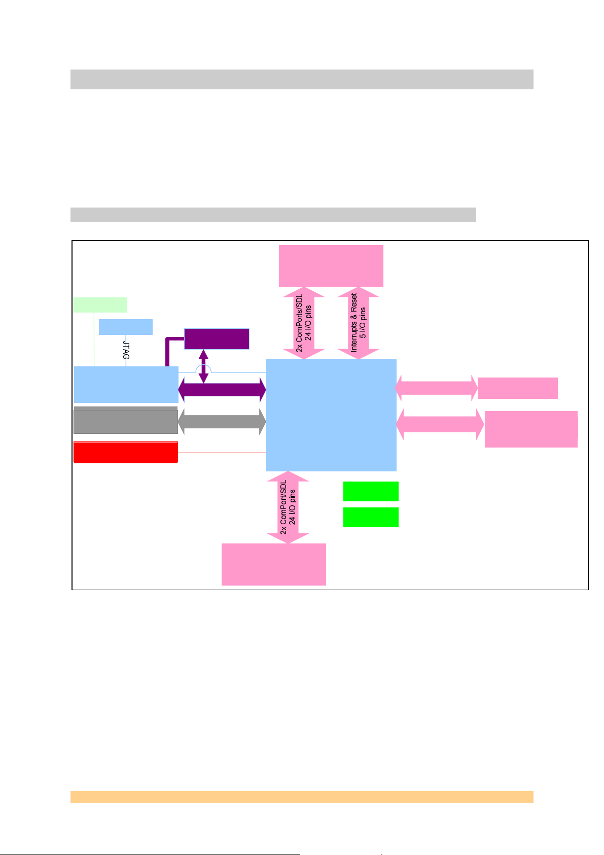
4.1 Block Diagram
Switch
JTAG Header
Xilinx Coolrunner II CPLD
XC2C256CP132 on
Comport3 and
Config&control
2 banks of
DDR2SDRAM
2x (64Mx16 or 128Mx16)
4 LEDs
Flash memory
11 I/O pins
204 I/O pins
J2 Bottom Secondary TIM
JTAG
Connector
ComPort/SDL 1 & 4
J1 Top Primary TIM
Connector
ComPort/SDL 0 & 3
FPGA
Virtex-5 FF1136
XC5V
SX50T/LX50T/
SX95T/LX110T
1.0V Core
1.8V/2.5V/3.3V I/O
RSL clock
Local clock
16 RocketIO links
20 differential pairs
40 TTL IOs
Sundance Rocket io
Serial Link (4 Conn.)
Sundance Low-voltage Bus
(1 Conn.)
ONLY with
LX160
Figure 1: Block Diagram
SMT351T User Guide Last Edited: 04/09/2009 11:26:00
Page 10

4.2 Module Description
Figure 1 presents colour coded blocks regrouping components according to their functionality or
their nature.
The following paragraphs will detail each one of them, but first, here is a global description of each
block.
• Block1 and Block6 Xilinx Virtex 5 XC5VSXT/LXT and configuration scheme for the FPGA.
• Block2: DDR2SDRAM memory banks.
• Block3: IO connectors for general purpose or dedicated interfaces.
• Block4: 50MHz or 125MHz clocks.
• Block5: LEDs for development and in-use monitoring and general purpose use.
4.2.1 FPGA
Xilinx Virtex 5 XC5VSX50T, XC5VLX50T, XC4VSX95T or XC5VLX110T FPGA.
This device is packaged in a FF1136-pin BGA package.
4.2.2 CPLD
Xilinx Coolrunner II device H19H19HHTUXC2C256-7CP132CUTHH.
This device is packaged in a 132-ball BGA type package with a -7 speed grade.
It can be used to configure the FGPA via Comport 3, or from a configuration stored in flash
memory.
The flash memory is programmed using the CPLD and via the ComPort3.
4.2.3 FLASH MEMORY
20H20HHS29GL256N11TFI01H is a 256Mbit flash from Spansion.
It can be used to configure the FPGA at power up.
Flash accessed using Comport3 via the CPLD.
Flash programming selection via switch SW1 (See X87H87HTable 3X)
Software Library Support available from Sundance.
The code can run on Sundance DSP TIM or a Host.
All the flash functionalities are available.
SMT351T User Guide Page 10 of 37 Last Edited: 04/09/2009 11:26:00
Page 11

4.2.4 JTAG Header
The JTAG header is compatible with Xilinx H21H21HHTUParallel-IVUTHH cable signals.
The header is a custom header that plugs onto a custom cable that must be ordered at time from
Sundance.
This cable then plugs into the Xilinx parallel cable pod.
It supportsT code download (for the FPGA), FPGA configuration, Hardware and Software
Debugging tools for the Virtex-5.
This cable connects the parallel port/USB port of an engineer's Workstation/PC to the JTAG
chain of the SMT351T Module.
All the Xilinx devices from block1 are chained and accessible via this JTAG header.
4.2.5 FPGA Configuration schemes
Different schemes are available to provide maximum flexibility in systems where the
SMT351T is involved:
The FPGA configuration bitstream source is
• On Comport 3:
The CPLD is connected to the Comport 3 link of the SMT351T TIM connector. (See block1).
A switch is used to select Comport 3 as the link that will be used to receive the bitstream.
The CPLD allows for FPGA configuration in slave SelectMAP mode.
• Using the on-board Flash memory.
The CPLD monitors the configuration data between the Flash and the FPGA.
The FPGA configuration is operated in Slave SelectMap mode.
A switch is used to select the Flash as the source for the configuration bitstream.
• Using the on-board JTAG header and Xilinx JTAG programming tools.
The JTAG header is a H22H22HHTUParallel-IVUTHH Header.
Note: Using JTAG to configure the FPGA bypasses the CPLD which controls configuration.
The following section describes the CPLD role and the reset scheme used.
As the CPLD is bypassed when JTAG is used to configure the FPGA, it is necessary to adopt
one of the three following ways:
SMT351T User Guide Page 11 of 37 Last Edited: 04/09/2009 11:26:00
Page 12

• If your FPGA design does not implement comport3,
o do not use the Reset signal generated by the CPLD but use the TIM reset signal
as your design’s reset. You can use JTAG to configure your FPGA with your
application and the design will reset and run everytime you issue a new TIM
reset.
• If your design implements comport3
o Set the switch to configure the FPGA from flash after reset. In this way a default
bitstream being stored in flash will be loaded in the FPGA by the CPLD.
In this manner the CPLD has gone trhough the cycle of configuring the
FPGA and releases the reset (FPGAresetn)
Then you can reconfigure the FPGA via JTAG with your application.
o Set the switch to configure from comport 3. After reset, configure the FPGA via
JTAG and provide an end key word on comport 3 to the CPLD so that it releases
the Reset. (FPGAresetn).
4.2.6 FPGA Reset Scheme
The CPLD is connected to a TIM global Reset signal provided to the SMT351T via its primary
TIM connector pin 30. (See 23H23HHTI TIM specification & User’s guideH).
This signal goes to the CPLD and the FPGA.
Nevertheless as a general rule for good practice, the FPGA should not use this reset but should
use the reset signal generated by the CPLD.
The CPLD provides another signal called FPGAResetn that offers a better Reset control over
the FPGA.
At power up or on reception of a low TIM global Reset pulse, the CPLD drives the
FPGAResetn signal low and keeps it low.
This is used to keep the FPGA design in reset.
A new FPGA configuration bitstream can then be downloaded.
When the ENDKEY has been received, the CPLD drives FPGAResetn high.
Use FPGAResetn for the Global Reset signal of your FPGA
designs.
In this manner, you can control your FPGA design Reset activity and you will also avoid
possible conflicts on ComPort 3 if your FPGA design implements it.
(Comport3 is a communication resource shared by the CPLD and the FPGA. But only 1 entity
is allowed to use it at a time).
SMT351T User Guide Page 12 of 37 Last Edited: 04/09/2009 11:26:00
Page 13

If you implement comport 3 in the FPGA you have to use
Fpgaresetn generated by the CPLD, as the comport is shared
between the two.
The Reset control is operated by the CPLD line FPGAResetn.
The following diagram shows the CPLD states after Reset.
Figure 2: CPLD state machine
SMT351T User Guide Page 13 of 37 Last Edited: 04/09/2009 11:26:00
Page 14

4.2.7 FPGA Bitstream formatting
If you generated you FPGA bitstream using Diamond FPGA, you do not need any other handling.
The .app file created can be used as is to configure the FPGA.
If you used Xilinx ISE and created a .bit file, you need to use the Sundance executable
“Getrawdata.exe” provided for free in the SMT6001 package.
Please read the SMT6001 help file at chapter: “Saving FPGA configuration data to file”.
The resulting file can be used as is to configure the FPGA.
4.2.8 DDR2SDRAM
There are 8 devices of DDR2 SDRAM connected to the FPGA providing up to 2GBytes of
storage.
The devices are grouped in two independent banks. The two banks are identical so we will
discuss only one.
A bank is made of four devices. Within a bank the devices share the same address and control
bus.
The data bus of each device is routed to the FPGA. This allows accessing all the chips in
parallel, at the same time.
The DDR2 memory runs at 200MHz with of the shelf controllers form MIG tools, but higher
performances can be reached if the designs are optimised.
Depending on the FPGA and design implemented, performances might vary.
Each bank is fully independent with separate address, control and data busses and arranged as
follows:
SMT351T User Guide Page 14 of 37 Last Edited: 04/09/2009 11:26:00
Page 15

ts
n
4x
compone
nts
x
e
4
n
ompo
c
Figure 3: FPGA connections to DDR2SDRAM
Xilinx MIG utility:
The Memory controllers generated by MIG1.72 and MIG2.0 have been successfully running at
200MHz.
The pinout was not generated using MIG2.0 but the controllers generated by MIG2.0 can be
used with the SMT351T pinout. Also see Xilinx 24H24HHAR#29313H
Xilinx issue bug fixes for their designs, and the controllers generated by MIG2.0 are not
exempt.
Please read these 2 answer records from Xilinx: HAR#30410H and HAR#29783H
and for simulation: HAR#29478H
The devices used are Micron 25H25HHDDR2SDRAM 1GbitH (MT47H64M16BT-37E) or
25H25HHDDR2SDRAM 2GbitH (MT47H128M16BT-37E) devicesH27H27HHTUUTHH.
SMT351T User Guide Page 15 of 37 Last Edited: 04/09/2009 11:26:00
Page 16

Alternative part numbers, fully compatible can be fitted depending on availability at time of
order.
4.2.9 Sundance Rocket io Serial Link
Sundance boards can be interconnected using RSL connectors located on the front and back of
the board. The SMT351T has four connectors in total (two at the front and two at the back).
The boards connected via RSL use the RSL protocol to communicate. Refer to the Sundance
Help File for more details.
The underlying design of the RSL uses the MGT of the FPGA to transfer the data. Each FPGA
has a different amount or MGTs. Some FPGAs do not have any MGTs; boards using these
cannot use the RSL protocol.
The speed of the RSL depends on the frequency at which the MGTs are clocked. Sundance
uses 125Mhz, allowing data rate of 2.5Gbits/s per MGT.
Depending on the FPGA fitted on the SMT351T up to 16 RSL links may be available.
The LX50T and SX50T FPGAs provide 12 links
The LX110T and SX95T FPGAs provide 16 links.
4.2.10 Sundance Low voltage Bus
The SLB bus is used to extend the functionality of the SMT351T by connecting to it a daughter
board.
There are different types of daughter boards. Some provide ADCs, some DACs or a
combination of both.
Sundance provides examples and reference design combining the SMT351T to daughter
boards. These examples are usually designed with 3L Diamond tools.
Electrical details
Typically, this is an LVDS bus comprising data (2 x 16 bit buses, I & Q), clock, and control
signals.
Nevertheless, the SLB lines can also be used for single ended signalling.
They allow interfacing to Sundance mezzanine modules providing that you implement an SLB
interface in the FPGA. (See X89H89H2.1X)
They allow interfacing to the outside world by implementing your own LVDS interface in the
FPGA.
In LVDS mode, all LVDS data pins (both I and Q) are connected to a 2.5V powered FPGA
bank (link selectable by jumper JP2).
SMT351T User Guide Page 16 of 37 Last Edited: 04/09/2009 11:26:00
Page 17

The FPGA LVDS DIFF_TERM standard should be used instead of the DCI terminations when
LVDS standard is selected.
DCI terminations are only available when a 2.5v standard is selected.
The LVDS Clock signals are also in these banks.
In LVTTL mode, all LVTTL signals are connected to a 3.3V powered FPGA bank.
(Link selectable by jumper JP2).
In case the SLB bus is to be used with a mezzanine, the SLB voltage
level must be set according to the mezzanine fitted on the module.
4.2.11 TIM Connectors
TIM connectors provide 4 communication links (Comports) and a Global Bus to the FPGA.
The comports which are available on the SMT351T are CP0, CP1, CP3, and CP4.
They allow interfacing to Sundance TIM modules or to a Host PC providing that you
implement a Comport Interface inside the FPGA. (See X90H90H2.1X)
The Comport interface is available in Sundance SMT6500 support package.
The FPGA io banks hosting the Comport signals are powered using Vcco = 3.3v.
The TIM connectors also provide power/ground, reset and various control signals.
References and specifications for these connectors are available in H28H28HHTUTI TIM specification &
user’s guideUTHH
4.2.12 DIP Switches
One four-position DIP switch is connected to the CPLD to provide control over the selection of
the configuration bitstream source and a special reset feature called “TIM Confign”.
SW1 pos 4 TIM Config
ON ENABLED
OFF DISABLED
Table 1: DIP switch SW1 position for special reset feature
SMT351T User Guide Page 17 of 37 Last Edited: 04/09/2009 11:26:00
Page 18

SW1 pos 3,2, 1 JPC3 JPC2 JPC1
C3P OFF OFF OFF
Flash boots from address 0 OFF OFF ON
Flash boots from address
0x800000
OFF ON ON
Table 2: DIP switch SW1 position for the selection of the configuration bitstream source
SW1 pos 3,2, 1 JPC3 JPC2 JPC1
Flash accesses ON OFF OFF
Table 3: DIP switch SW1 position for the selection of the Flash erase & program operations.
The Flash erase & program operations are operated by the CPLD.
Commands are provided via Comport3 from an application running on a Host or DSP.
On the Host, this application is the SMT6002, please ask Sundance as it is not yet available
under the Sundance Wizzard.
Status information from the Flash is given over Comport3 as well.
4.2.13 Available clocks
Two onboard clocks:
• 50mhz LVTTL oscillator. Used by the CPLD and connected to the FPGA.
• 125mhz LVDS oscillator. Connected to the FPGA. Used to clock the MGTs.
An external clock can be input into the Virtex 5 FPGA via the SLB connector.
Sundance applies this scheme for ADC/DAC mezzanines.
SMT351T User Guide Page 18 of 37 Last Edited: 04/09/2009 11:26:00
Page 19

Global clock input, (for single ended
clocks, or for differential clocks, P side)
Regional clock input, (for single ended
clocks, or for differential clocks, P side)
LEFT COLUMN
MIDDLE
COLUMN
RIGHT COLUMN
1
BANK
BANK 13 BANK 15
DDR2B
BANK 21 BANK 17
1
BANK
DDR2A
d
q
s
0
d
q
s
0
d
q
s
2
d
q
s
1
BANK 19
BANK 15
BANK 11
BANK 17
d
q
s
5
d
q
s
4
d
q
s
7
d
q
s
2
d
q
s
1
d
q
s
0
d
q
s
3
d
q
s
6
d
q
s
4
d
q
s
7
d
q
s
5
d
q
s
3
d
q
s
6
g
2
7
h
2
8
e
2
8
k31
k
3
1
p
3
1
m
3
1
h
3
4
k
3
3
a
f
3
4
a
h
3
4
a
d
3
2
y
2
8
a
a
2
9
a
k
2
6
a
k
2
9
a
k
2
8
BANK 23BANK 19BANK 15BANK 11
BANK 13BANK 17BANK 21
BANK 5
BANK
BANK
BANK
BANK
pxiclk
BANK 20
3
1
2
ag21
4
vclk_p
osc50
ag18
j6
BANK 12
BANK 18BANK 22
Clkouti_p
w6
Clkoutq_p
BANK 25
TIM Conn
PXICLK
50Mhz single ended
osc
BANK 6
125MHz differential
oscillator
Figure 4: FPGA clock buffers usage.
SMT351T User Guide Page 19 of 37 Last Edited: 04/09/2009 11:26:00
Page 20

4.2.14 LEDs
4 Red LEDs connect to the FPGA and are available to the User: D4, D5, D6, D7.
1 Green Led: D1, connects to the DONE pin of the FPGA and is lit to show that the FPGA is
configured. (depending on supply from manufacturer a red led can be fitted instead).
4.2.15 Performance
The FPGA features like speed grade and density dictate most performances.
The performances achievable by the other components are given in the chapters above and
the components respective data sheets.
4.3 Interface Description
For the TIM to carrier board or external world interfacing, see in H29H29HHTUSundance Help fileUTHH (that you
can download from the Sundance Wizzard)
4.3.1 Power Budget
The SMT351T draws its power from the 3.3v rail of the PCI.
The PCI specification stipulates that the maximum power for one card is 25W.
Therefore, the maximum current that the SMT351T could draw from +3.3V is 7.6A, assuming
zero current on all the other supply voltages.
But this limit is "system dependent," so a given system might not have the full 7.6A available
for a slot even if it is the only PCI card in the system.
A system might balance the power capabilities differently between the +5V and +3.3V (and +/-
12V) supplies, rather than making 25W available from +5V and 25W available from +3.3V.
As a result, check your main power supply ratings.
If your system is likely to reach 25W per power rail we advice that you provide extra power to
the carrier board using an external power supply.
SMT351T User Guide Page 20 of 37 Last Edited: 04/09/2009 11:26:00
Page 21

Details:
Coolrunner XC2C256-6-CP132 power requirements based on design:
Macrocells
Used
218/256 (86%) 531/896 (60%) 190/256 (75%) 69/106 (66%) 445/640 (70%)
Pterms Used Registers Used Pins Used
Function Block
Inputs Used
Table 4: Coolrunner II resources summary.
Signal Type Required Mapped
Input 8 8
Output 40 40
Bidirectional 20 20
GCK 1 1
GTS 0 0
GSR 0 0
Pin Type Used Total
I/O 65 96
GCK/IO 3 3
GTS/IO 0 4
GSR/IO 1 1
CDR/IO 0 1
DGE/IO 0 1
Table 5:Coolrunner II pin resources.
SMT351T User Guide Last Edited: 04/09/2009 11:26:00
Page 22

5 Footprint
5.1 Top View
Primary TIM connector Secondary TIM connector
SLB Connector
Jumper JP2 Selection of
voltage level for SLB
interface
RSL Connector
Configuration switch
DDR2 SDRAM Memory
JTAG header
Oscillator
FPGACPLD
RSL Connector
Figure 5: Top View
SMT351T User Guide Last Edited: 04/09/2009 11:26:00
Page 23

5.2 Bottom View
Figure 6: Bottom view
SMT351T User Guide Last Edited: 04/09/2009 11:26:00
Page 24

6 Pinout
6.1 FPGA Pin allocation by bank
5vlx110tff1136
Regional Clock Inputs (for single ended clocks, or for differential clocks, P side)
Regional Clock Inputs (for differential clocks only, N side)
Pin Name Signal Name Bank Pad Name Slice X/Y I/O Name
K24 DDRA_D58 19 IOB_X0Y279 X0Y139 IO_L0P_19 X0Y6
L24 DDRA_D59 19 IOB_X0Y278 X0Y139 IO_L0N_19
L25 DDRA_D42 19 IOB_X0Y277 X0Y138 IO_L1P_19
L26 DDRA_D36 19 IOB_X0Y276 X0Y138 IO_L1N_19
J24 DDRA_D57 19 IOB_X0Y275 X0Y137 IO_L2P_19
J25 DDRA_D35 19 IOB_X0Y274 X0Y137 IO_L2N_19
M25 DDRA_D41 19 IOB_X0Y273 X0Y136 IO_L3P_19
M26 DDRA_D37 19 IOB_X0Y272 X0Y136 IO_L3N_19
J27 DDRA_D44 19 IOB_X0Y271 X0Y135 IO_L4P_19
J26 19 IOB_X0Y270 X0Y135 IO_L4N_VREF_19
G25 DDRA_D43 19 IOB_X0Y269 X0Y134 IO_L5P_19
G26 DDRA_D33 19 IOB_X0Y268 X0Y134 IO_L5N_19
H25 DDRA_D34 19 IOB_X0Y267 X0Y133 IO_L6P_19
H24 DDRA_D56 19 IOB_X0Y266 X0Y133 IO_L6N_19
F25 DDRA_D40 19 IOB_X0Y265 X0Y132 IO_L7P_19
F26 DDRA_D32 19 IOB_X0Y264 X0Y132 IO_L7N_19
G27 DDRA_DQS5 19 IOB_X0Y263 X0Y131 IO_L8P_CC_19
H27 DDRA_NDQS5 19 IOB_X0Y262 X0Y131 IO_L8N_CC_19
H28 DDRA_DQS4 19 IOB_X0Y261 X0Y130 IO_L9P_CC_19
G28 DDRA_NDQS4 19 IOB_X0Y260 X0Y130 IO_L9N_CC_19
E28 DDRA_DQS7 19 IOB_X0Y259 X0Y129 IO_L10P_CC_19
F28 DDRA_NDQS7 19 IOB_X0Y258 X0Y129 IO_L10N_CC_19
E26 DDRA_DM0 19 IOB_X0Y257 X0Y128 IO_L11P_CC_19
E27 DDRA_DM7 19 IOB_X0Y256 X0Y128 IO_L11N_CC_19
N27 19 IOB_X0Y255 X0Y127 IO_L12P_VRN_19
M27 19 IOB_X0Y254 X0Y127 IO_L12N_VRP_19
K28 DDRA_CLK 19 IOB_X0Y253 X0Y126 IO_L13P_19
L28 DDRA_NCLK 19 IOB_X0Y252 X0Y126 IO_L13N_19
K27 DDRA_D45 19 IOB_X0Y251 X0Y125 IO_L14P_19
K26 19 IOB_X0Y250 X0Y125 IO_L14N_VREF_19
M28 DDRA_NWE 19 IOB_X0Y249 X0Y124 IO_L15P_19
N28 DDRA_A6 19 IOB_X0Y248 X0Y124 IO_L15N_19
P26 DDRA_D38 19 IOB_X0Y247 X0Y123 IO_L16P_19
P27 DDRA_D39 19 IOB_X0Y246 X0Y123 IO_L16N_19
N24 DDRA_D60 19 IOB_X0Y245 X0Y122 IO_L17P_19
P24 DDRA_D61 19 IOB_X0Y244 X0Y122 IO_L17N_19
P25 DDRA_D47 19 IOB_X0Y243 X0Y121 IO_L18P_19
N25 DDRA_D46 19 IOB_X0Y242 X0Y121 IO_L18N_19
R24 DDRA_D62 19 IOB_X0Y241 X0Y120 IO_L19P_19
T24 DDRA_D63 19 IOB_X0Y240 X0Y120 IO_L19N_19
E29 DDRA_D23 15 IOB_X0Y239 X0Y119 IO_L0P_15 X0Y5
F29 DDRA_D22 15 IOB_X0Y238 X0Y119 IO_L0N_15
G30 DDRA_D21 15 IOB_X0Y237 X0Y118 IO_L1P_15
F30 DDRA_D20 15 IOB_X0Y236 X0Y118 IO_L1N_15
H29 DDRA_D19 15 IOB_X0Y235 X0Y117 IO_L2P_15
J29 DDRA_D18 15 IOB_X0Y234 X0Y117 IO_L2N_15
F31 DDRA_D17 15 IOB_X0Y233 X0Y116 IO_L3P_15
E31 DDRA_D16 15 IOB_X0Y232 X0Y116 IO_L3N_15
L29 DDRA_D15 15 IOB_X0Y231 X0Y115 IO_L4P_15
K29 15 IOB_X0Y230 X0Y115 IO_L4N_VREF_15
H30 DDRA_D14 15 IOB_X0Y229 X0Y114 IO_L5P_15
G31 DDRA_D13 15 IOB_X0Y228 X0Y114 IO_L5N_15
J30 DDRA_D12 15 IOB_X0Y227 X0Y113 IO_L6P_15
J31 DDRA_D11 15 IOB_X0Y226 X0Y113 IO_L6N_15
L30 DDRA_D10 15 IOB_X0Y225 X0Y112 IO_L7P_15
Clock
Region
SMT351T User Guide Last Edited: 04/09/2009 11:26:00
Page 25

M30 DDRA_D9 15 IOB_X0Y224 X0Y112 IO_L7N_15
N29 DDRA_D8 15 IOB_X0Y223 X0Y111 IO_L8P_CC_15
P29 DDRA_A8 15 IOB_X0Y222 X0Y111 IO_L8N_CC_15
K31 DDRA_DQS2 15 IOB_X0Y221 X0Y110 IO_L9P_CC_15
L31 DDRA_NDQS2 15 IOB_X0Y220 X0Y110 IO_L9N_CC_15
P31 DDRA_DQS1 15 IOB_X0Y219 X0Y109 IO_L10P_CC_15
P30 DDRA_NDQS1 15 IOB_X0Y218 X0Y109 IO_L10N_CC_15
M31 DDRA_DQS0 15 IOB_X0Y217 X0Y108 IO_L11P_CC_15
N30 DDRA_NDQS0 15 IOB_X0Y216 X0Y108 IO_L11N_CC_15
R28 15 IOB_X0Y215 X0Y107 IO_L12P_VRN_15
R29 15 IOB_X0Y214 X0Y107 IO_L12N_VRP_15
T31 DDRB_A0 15 IOB_X0Y213 X0Y106 IO_L13P_15
R31 DDRA_A2 15 IOB_X0Y212 X0Y106 IO_L13N_15
U30 DDRA_A12 15 IOB_X0Y211 X0Y105 IO_L14P_15
T30 15 IOB_X0Y210 X0Y105 IO_L14N_VREF_15
T28 DDRA_A10 15 IOB_X0Y209 X0Y104 IO_L15P_15
T29 DDRA_A1 15 IOB_X0Y208 X0Y104 IO_L15N_15
U27 DDRA_D7 15 IOB_X0Y207 X0Y103 IO_L16P_15
U28 DDRA_D6 15 IOB_X0Y206 X0Y103 IO_L16N_15
R26 DDRA_D5 15 IOB_X0Y205 X0Y102 IO_L17P_15
R27 DDRA_D4 15 IOB_X0Y204 X0Y102 IO_L17N_15
U26 DDRA_D3 15 IOB_X0Y203 X0Y101 IO_L18P_15
T26 DDRA_D2 15 IOB_X0Y202 X0Y101 IO_L18N_15
U25 DDRA_D1 15 IOB_X0Y201 X0Y100 IO_L19P_15
T25 DDRA_D0 15 IOB_X0Y200 X0Y100 IO_L19N_15
B32 DDRA_A13 11 IOB_X0Y199 X0Y99 IO_L0P_11 X0Y4
A33 DDRA_DM6 11 IOB_X0Y198 X0Y99 IO_L0N_11
B33 DDRA_BA2 11 IOB_X0Y197 X0Y98 IO_L1P_11
C33 DDRA_NRAS 11 IOB_X0Y196 X0Y98 IO_L1N_11
C32 DDRA_A14 11 IOB_X0Y195 X0Y97 IO_L2P_11
D32 DDRA_A9 11 IOB_X0Y194 X0Y97 IO_L2N_11
C34 DDRA_BA1 11 IOB_X0Y193 X0Y96 IO_L3P_11
D34 DDRA_A7 11 IOB_X0Y192 X0Y96 IO_L3N_11
G32 DDRA_D31 11 IOB_X0Y191 X0Y95 IO_L4P_11
H32 11 IOB_X0Y190 X0Y95 IO_L4N_VREF_11
F33 DDRA_D30 11 IOB_X0Y189 X0Y94 IO_L5P_11
E34 DDRA_D29 11 IOB_X0Y188 X0Y94 IO_L5N_11
E32 DDRA_D28 11 IOB_X0Y187 X0Y93 IO_L6P_11
E33 DDRA_D27 11 IOB_X0Y186 X0Y93 IO_L6N_11
G33 DDRA_D26 11 IOB_X0Y185 X0Y92 IO_L7P_11
F34 DDRA_D25 11 IOB_X0Y184 X0Y92 IO_L7N_11
J32 DDRA_D24 11 IOB_X0Y183 X0Y91 IO_L8P_CC_11
H33 DDRA_A5 11 IOB_X0Y182 X0Y91 IO_L8N_CC_11
H34 DDRA_DQS3 11 IOB_X0Y181 X0Y90 IO_L9P_CC_11
J34 DDRA_NDQS3 11 IOB_X0Y180 X0Y90 IO_L9N_CC_11
L34 DDRA_NCAS 11 IOB_X0Y179 X0Y89 IO_L10P_CC_SM15P_11
K34 DDRA_BA0 11 IOB_X0Y178 X0Y89 IO_L10N_CC_SM15N_11
K33 DDRA_DQS6 11 IOB_X0Y177 X0Y88 IO_L11P_CC_SM14P_11
K32 DDRA_NDQS6 11 IOB_X0Y176 X0Y88 IO_L11N_CC_SM14N_11
N33 11 IOB_X0Y175 X0Y87 IO_L12P_VRN_11
M33 11 IOB_X0Y174 X0Y87 IO_L12N_VRP_11
L33 DDRA_A15 11 IOB_X0Y173 X0Y86 IO_L13P_11
M32 DDRA_A11 11 IOB_X0Y172 X0Y86 IO_L13N_11
P34 DDRA_A4 11 IOB_X0Y171 X0Y85 IO_L14P_11
N34 11 IOB_X0Y170 X0Y85 IO_L14N_VREF_11
P32 DDRA_A3 11 IOB_X0Y169 X0Y84 IO_L15P_SM13P_11
N32 11 IOB_X0Y168 X0Y84 IO_L15N_SM13N_11
T33 DDRA_D55 11 IOB_X0Y167 X0Y83 IO_L16P_SM12P_11
R34 DDRA_D54 11 IOB_X0Y166 X0Y83 IO_L16N_SM12N_11
R33 DDRA_D53 11 IOB_X0Y165 X0Y82 IO_L17P_SM11P_11
R32 DDRA_D52 11 IOB_X0Y164 X0Y82 IO_L17N_SM11N_11
U33 DDRA_D51 11 IOB_X0Y163 X0Y81 IO_L18P_SM10P_11
T34 DDRA_D50 11 IOB_X0Y162 X0Y81 IO_L18N_SM10N_11
U32 DDRA_D49 11 IOB_X0Y161 X0Y80 IO_L19P_SM9P_11
U31 DDRA_D48 11 IOB_X0Y160 X0Y80 IO_L19N_SM9N_11
V32 DDRB_D39 13 IOB_X0Y159 X0Y79 IO_L0P_SM8P_13 X0Y3
V33 DDRB_D38 13 IOB_X0Y158 X0Y79 IO_L0N_SM8N_13
W34 DDRB_D37 13 IOB_X0Y157 X0Y78 IO_L1P_SM7P_13
SMT351T User Guide Page 25 of 37 Last Edited: 04/09/2009 11:26:00
Page 26

V34 DDRB_D36 13 IOB_X0Y156 X0Y78 IO_L1N_SM7N_13
Y33 DDRB_D35 13 IOB_X0Y155 X0Y77 IO_L2P_SM6P_13
AA33 DDRB_D33 13 IOB_X0Y154 X0Y77 IO_L2N_SM6N_13
AA34 DDRB_D34 13 IOB_X0Y153 X0Y76 IO_L3P_SM5P_13
Y34 DDRB_D32 13 IOB_X0Y152 X0Y76 IO_L3N_SM5N_13
Y32 DDRB_D63 13 IOB_X0Y151 X0Y75 IO_L4P_13
W32 13 IOB_X0Y150 X0Y75 IO_L4N_VREF_13
AC34 DDRB_D62 13 IOB_X0Y149 X0Y74 IO_L5P_SM4P_13
AD34 DDRB_D61 13 IOB_X0Y148 X0Y74 IO_L5N_SM4N_13
AC32 DDRB_D60 13 IOB_X0Y147 X0Y73 IO_L6P_SM3P_13
AB32 DDRB_D59 13 IOB_X0Y146 X0Y73 IO_L6N_SM3N_13
AC33 DDRB_D58 13 IOB_X0Y145 X0Y72 IO_L7P_SM2P_13
AB33 DDRB_D57 13 IOB_X0Y144 X0Y72 IO_L7N_SM2N_13
AF33 DDRB_D56 13 IOB_X0Y143 X0Y71 IO_L8P_CC_SM1P_13
AE33 DDRB_NRAS 13 IOB_X0Y142 X0Y71 IO_L8N_CC_SM1N_13
AF34 DDRB_DQS4 13 IOB_X0Y141 X0Y70 IO_L9P_CC_SM0P_13
AE34 DDRB_NDQS4 13 IOB_X0Y140 X0Y70 IO_L9N_CC_SM0N_13
AH34 DDRB_DQS7 13 IOB_X0Y139 X0Y69 IO_L10P_CC_13
AJ34 DDRB_NDQS7 13 IOB_X0Y138 X0Y69 IO_L10N_CC_13
AD32 DDRB_DQS5 13 IOB_X0Y137 X0Y68 IO_L11P_CC_13
AE32 DDRB_NDQS5 13 IOB_X0Y136 X0Y68 IO_L11N_CC_13
AG33 13 IOB_X0Y135 X0Y67 IO_L12P_VRN_13
AH33 13 IOB_X0Y134 X0Y67 IO_L12N_VRP_13
AK34 DDRB_A9 13 IOB_X0Y133 X0Y66 IO_L13P_13
AK33 DDRB_A8 13 IOB_X0Y132 X0Y66 IO_L13N_13
AG32 DDRB_A15 13 IOB_X0Y131 X0Y65 IO_L14P_13
AH32 13 IOB_X0Y130 X0Y65 IO_L14N_VREF_13
AJ32 DDRB_NCAS 13 IOB_X0Y129 X0Y64 IO_L15P_13
AK32 DDRB_A13 13 IOB_X0Y128 X0Y64 IO_L15N_13
AL34 DDRB_D47 13 IOB_X0Y127 X0Y63 IO_L16P_13
AL33 DDRB_D46 13 IOB_X0Y126 X0Y63 IO_L16N_13
AM33 DDRB_D45 13 IOB_X0Y125 X0Y62 IO_L17P_13
AM32 DDRB_D44 13 IOB_X0Y124 X0Y62 IO_L17N_13
AN34 DDRB_D43 13 IOB_X0Y123 X0Y61 IO_L18P_13
AN33 DDRB_D42 13 IOB_X0Y122 X0Y61 IO_L18N_13
AN32 DDRB_D41 13 IOB_X0Y121 X0Y60 IO_L19P_13
AP32 DDRB_D40 13 IOB_X0Y120 X0Y60 IO_L19N_13
W24 DDRA_DM4 17 IOB_X0Y119 X0Y59 IO_L0P_17 X0Y2
V24 DDRB_A3 17 IOB_X0Y118 X0Y59 IO_L0N_17
Y26 DDRB_D55 17 IOB_X0Y117 X0Y58 IO_L1P_17
W26 DDRB_BA0 17 IOB_X0Y116 X0Y58 IO_L1N_17
V25 DDRB_A10 17 IOB_X0Y115 X0Y57 IO_L2P_17
W25 DDRA_DM3 17 IOB_X0Y114 X0Y57 IO_L2N_17
Y27 DDRA_ODT 17 IOB_X0Y113 X0Y56 IO_L3P_17
W27 DDRB_BA2 17 IOB_X0Y112 X0Y56 IO_L3N_17
V30 DDRB_A5 17 IOB_X0Y111 X0Y55 IO_L4P_17
W30 17 IOB_X0Y110 X0Y55 IO_L4N_VREF_17
V28 DDRB_A4 17 IOB_X0Y109 X0Y54 IO_L5P_17
V27 DDRA_CKE 17 IOB_X0Y108 X0Y54 IO_L5N_17
W31 DDRB_D24 17 IOB_X0Y107 X0Y53 IO_L6P_17
Y31 DDRB_D25 17 IOB_X0Y106 X0Y53 IO_L6N_17
W29 DDRB_D49 17 IOB_X0Y105 X0Y52 IO_L7P_17
V29 DDRB_D48 17 IOB_X0Y104 X0Y52 IO_L7N_17
Y28 DDRB_DQS3 17 IOB_X0Y103 X0Y51 IO_L8P_CC_17
Y29 DDRB_NDQS3 17 IOB_X0Y102 X0Y51 IO_L8N_CC_17
AB31 DDRB_D27 17 IOB_X0Y101 X0Y50 IO_L9P_CC_17
AA31 DDRB_D26 17 IOB_X0Y100 X0Y50 IO_L9N_CC_17
AB30 DDRB_NWE 17 IOB_X0Y99 X0Y49 IO_L10P_CC_17
AC30 DDRB_A11 17 IOB_X0Y98 X0Y49 IO_L10N_CC_17
AA29 DDRB_DQS6 17 IOB_X0Y97 X0Y48 IO_L11P_CC_17
AA30 DDRB_NDQS6 17 IOB_X0Y96 X0Y48 IO_L11N_CC_17
AD31 17 IOB_X0Y95 X0Y47 IO_L12P_VRN_17
AE31 17 IOB_X0Y94 X0Y47 IO_L12N_VRP_17
AD30 DDRB_D28 17 IOB_X0Y93 X0Y46 IO_L13P_17
AC29 DDRB_D50 17 IOB_X0Y92 X0Y46 IO_L13N_17
AF31 DDRB_D30 17 IOB_X0Y91 X0Y45 IO_L14P_17
AG31 17 IOB_X0Y90 X0Y45 IO_L14N_VREF_17
AE29 DDRB_D52 17 IOB_X0Y89 X0Y44 IO_L15P_17
SMT351T User Guide Page 26 of 37 Last Edited: 04/09/2009 11:26:00
Page 27

AD29 DDRB_D51 17 IOB_X0Y88 X0Y44 IO_L15N_17
AJ31 DDRB_CLK 17 IOB_X0Y87 X0Y43 IO_L16P_17
AK31 DDRB_NCLK 17 IOB_X0Y86 X0Y43 IO_L16N_17
AF29 DDRB_D53 17 IOB_X0Y85 X0Y42 IO_L17P_17
AF30 DDRB_D29 17 IOB_X0Y84 X0Y42 IO_L17N_17
AJ30 DDRB_A12 17 IOB_X0Y83 X0Y41 IO_L18P_17
AH30 DDRB_A7 17 IOB_X0Y82 X0Y41 IO_L18N_17
AH29 DDRB_D54 17 IOB_X0Y81 X0Y40 IO_L19P_17
AG30 DDRB_D31 17 IOB_X0Y80 X0Y40 IO_L19N_17
AA25 DDRB_D2 21 IOB_X0Y79 X0Y39 IO_L0P_21 X0Y1
AA26 DDRB_A14 21 IOB_X0Y78 X0Y39 IO_L0N_21
AB27 DDRB_D15 21 IOB_X0Y77 X0Y38 IO_L1P_21
AC27 DDRB_D16 21 IOB_X0Y76 X0Y38 IO_L1N_21
Y24 DDRB_A1 21 IOB_X0Y75 X0Y37 IO_L2P_21
AA24 DDRB_A2 21 IOB_X0Y74 X0Y37 IO_L2N_21
AB25 DDRB_D3 21 IOB_X0Y73 X0Y36 IO_L3P_21
AB26 DDRB_A6 21 IOB_X0Y72 X0Y36 IO_L3N_21
AC28 DDRB_D10 21 IOB_X0Y71 X0Y35 IO_L4P_21
AD27 21 IOB_X0Y70 X0Y35 IO_L4N_VREF_21
AB28 DDRB_D9 21 IOB_X0Y69 X0Y34 IO_L5P_21
AA28 DDRB_D8 21 IOB_X0Y68 X0Y34 IO_L5N_21
AG28 DDRB_D13 21 IOB_X0Y67 X0Y33 IO_L6P_21
AH28 DDRB_D14 21 IOB_X0Y66 X0Y33 IO_L6N_21
AE28 DDRB_D11 21 IOB_X0Y65 X0Y32 IO_L7P_21
AF28 DDRB_D12 21 IOB_X0Y64 X0Y32 IO_L7N_21
AK26 DDRB_DQS0 21 IOB_X0Y63 X0Y31 IO_L8P_CC_21
AJ27 DDRB_NDQS0 21 IOB_X0Y62 X0Y31 IO_L8N_CC_21
AK29 DDRB_DQS2 21 IOB_X0Y61 X0Y30 IO_L9P_CC_21
AJ29 DDRB_NDQS2 21 IOB_X0Y60 X0Y30 IO_L9N_CC_21
AK28 DDRB_DQS1 21 IOB_X0Y59 X0Y29 IO_L10P_CC_21
AK27 DDRB_NDQS1 21 IOB_X0Y58 X0Y29 IO_L10N_CC_21
AH27 DDRB_D20 21 IOB_X0Y57 X0Y28 IO_L11P_CC_21
AJ26 DDRB_ODT 21 IOB_X0Y56 X0Y28 IO_L11N_CC_21
AJ25 21 IOB_X0Y55 X0Y27 IO_L12P_VRN_21
AH25 21 IOB_X0Y54 X0Y27 IO_L12N_VRP_21
AF24 DDRB_D1 21 IOB_X0Y53 X0Y26 IO_L13P_21
AG25 DDRB_D7 21 IOB_X0Y52 X0Y26 IO_L13N_21
AG27 DDRB_D19 21 IOB_X0Y51 X0Y25 IO_L14P_21
AG26 21 IOB_X0Y50 X0Y25 IO_L14N_VREF_21
AF25 DDRB_D6 21 IOB_X0Y49 X0Y24 IO_L15P_21
AF26 DDRB_D23 21 IOB_X0Y48 X0Y24 IO_L15N_21
AE27 DDRB_D18 21 IOB_X0Y47 X0Y23 IO_L16P_21
AE26 DDRB_D22 21 IOB_X0Y46 X0Y23 IO_L16N_21
AC25 DDRB_D4 21 IOB_X0Y45 X0Y22 IO_L17P_21
AC24 DDRB_BA1 21 IOB_X0Y44 X0Y22 IO_L17N_21
AD26 DDRB_D21 21 IOB_X0Y43 X0Y21 IO_L18P_21
AD25 DDRB_D5 21 IOB_X0Y42 X0Y21 IO_L18N_21
AD24 DDRB_D17 21 IOB_X0Y41 X0Y20 IO_L19P_21
AE24 DDRB_D0 21 IOB_X0Y40 X0Y20 IO_L19N_21
H17 TCLK0 3 IOB_X1Y219 X48Y109 IO_L0P_CC_GC_3 X0Y5
H18 TCLK1 3 IOB_X1Y218 X47Y109 IO_L0N_CC_GC_3
K17 IACK 3 IOB_X1Y217 X48Y108 IO_L1P_CC_GC_3
L18 NMI 3 IOB_X1Y216 X47Y108 IO_L1N_CC_GC_3
G15 RESET 3 IOB_X1Y215 X48Y107 IO_L2P_GC_VRN_3
G16 IIOF0 3 IOB_X1Y214 X47Y107 IO_L2N_GC_VRP_3
K18 IIOF1 3 IOB_X1Y213 X48Y106 IO_L3P_GC_3
J19 IIOF2 3 IOB_X1Y212 X47Y106 IO_L3N_GC_3
J16 3 IOB_X1Y211 X48Y105 IO_L4P_GC_3
J17 CONFIG 3 IOB_X1Y210 X47Y105 IO_L4N_GC_VREF_3
L19 3 IOB_X1Y209 X48Y104 IO_L5P_GC_3
K19 RESETFROMCPLD 3 IOB_X1Y208 X47Y104 IO_L5N_GC_3
H14 SWITCH0 3 IOB_X1Y207 X48Y103 IO_L6P_GC_3
H15 SWITCH1 3 IOB_X1Y206 X47Y103 IO_L6N_GC_3
J20 SWITCH2 3 IOB_X1Y205 X48Y102 IO_L7P_GC_3
J21 SWITCH3 3 IOB_X1Y204 X47Y102 IO_L7N_GC_3
J14 LED0 3 IOB_X1Y203 X48Y101 IO_L8P_GC_3
H13 LED1 3 IOB_X1Y202 X47Y101 IO_L8N_GC_3
H19 LED2 3 IOB_X1Y201 X48Y100 IO_L9P_GC_3
SMT351T User Guide Page 27 of 37 Last Edited: 04/09/2009 11:26:00
Page 28
H20 LED3 3 IOB_X1Y200 X47Y100 IO_L9N_GC_3
L21 DDRA_DM2 1 IOB_X1Y199 X48Y99 IO_L0P_A19_1 X0Y4
L20 DDRA_A0 1 IOB_X1Y198 X47Y99 IO_L0N_A18_1
L15 DDRB_DM2 1 IOB_X1Y197 X48Y98 IO_L1P_A17_1
L16 DDRB_DM1 1 IOB_X1Y196 X47Y98 IO_L1N_A16_1
J22 DDRB_NCS 1 IOB_X1Y195 X48Y97 IO_L2P_A15_D31_1
K21 DDRA_NCS 1 IOB_X1Y194 X47Y97 IO_L2N_A14_D30_1
K16 1 IOB_X1Y193 X48Y96 IO_L3P_A13_D29_1
J15 1 IOB_X1Y192 X47Y96 IO_L3N_A12_D28_1
G22 DDRB_CKE 1 IOB_X1Y191 X48Y95 IO_L4P_A11_D27_1
H22 1 IOB_X1Y190 X47Y95 IO_L4N_VREF_A10_D26_1
L14 DDRA_DM1 1 IOB_X1Y189 X48Y94 IO_L5P_A9_D25_1
K14 DDRB_DM0 1 IOB_X1Y188 X47Y94 IO_L5N_A8_D24_1
K23 DDRB_DM7 1 IOB_X1Y187 X48Y93 IO_L6P_A7_D23_1
K22 DDRA_DM5 1 IOB_X1Y186 X47Y93 IO_L6N_A6_D22_1
J12 DDRB_DM4 1 IOB_X1Y185 X48Y92 IO_L7P_A5_D21_1
H12 DDRB_DM5 1 IOB_X1Y184 X47Y92 IO_L7N_A4_D20_1
G23 1 IOB_X1Y183 X48Y91 IO_L8P_CC_A3_D19_1
H23 1 IOB_X1Y182 X47Y91 IO_L8N_CC_A2_D18_1
K13 DDRB_DM3 1 IOB_X1Y181 X48Y90 IO_L9P_CC_A1_D17_1
K12 DDRB_DM6 1 IOB_X1Y180 X47Y90 IO_L9N_CC_A0_D16_1
AE13 2 IOB_X1Y139 X48Y69 IO_L0P_CC_RS1_2 X0Y3
AE12 2 IOB_X1Y138 X47Y69 IO_L0N_CC_RS0_2
AF23 2 IOB_X1Y137 X48Y68 IO_L1P_CC_A25_2
AG23 2 IOB_X1Y136 X47Y68 IO_L1N_CC_A24_2
AF13 2 IOB_X1Y135 X48Y67 IO_L2P_A23_2
AG12 2 IOB_X1Y134 X47Y67 IO_L2N_A22_2
AE22 2 IOB_X1Y133 X48Y66 IO_L3P_A21_2
AE23 2 IOB_X1Y132 X47Y66 IO_L3N_A20_2
AE14 2 IOB_X1Y131 X48Y65 IO_L4P_FCS_B_2
AF14 2 IOB_X1Y130 X47Y65 IO_L4N_VREF_FOE_B_MOSI_2
AF20 2 IOB_X1Y129 X48Y64 IO_L5P_FWE_B_2
AF21 2 IOB_X1Y128 X47Y64 IO_L5N_CSO_B_2
AF15 FLASH_D7 2 IOB_X1Y127 X48Y63 IO_L6P_D7_2
AE16 FLASH_D6 2 IOB_X1Y126 X47Y63 IO_L6N_D6_2
AE21 FLASH_D5 2 IOB_X1Y125 X48Y62 IO_L7P_D5_2
AD20 FLASH_D4 2 IOB_X1Y124 X47Y62 IO_L7N_D4_2
AF16 FLASH_D3 2 IOB_X1Y123 X48Y61 IO_L8P_D3_2
AE17 FLASH_D2 2 IOB_X1Y122 X47Y61 IO_L8N_D2_FS2_2
AE19 FLASH_D1 2 IOB_X1Y121 X48Y60 IO_L9P_D1_FS1_2
AD19 FLASH_D0 2 IOB_X1Y120 X47Y60 IO_L9N_D0_FS0_2
AG22 C4D4 4 IOB_X1Y119 X48Y59 IO_L0P_GC_D15_4 X0Y2
AH22 C4D5 4 IOB_X1Y118 X47Y59 IO_L0N_GC_D14_4
AH12 C4D6 4 IOB_X1Y117 X48Y58 IO_L1P_GC_D13_4
AG13 C4D7 4 IOB_X1Y116 X47Y58 IO_L1N_GC_D12_4
AH20 C4D0 4 IOB_X1Y115 X48Y57 IO_L2P_GC_D11_4
AH19 C4D1 4 IOB_X1Y114 X47Y57 IO_L2N_GC_D10_4
AH14 C4D2 4 IOB_X1Y113 X48Y56 IO_L3P_GC_D9_4
AH13 C4D3 4 IOB_X1Y112 X47Y56 IO_L3N_GC_D8_4
AG21 OSC50 4 IOB_X1Y111 X48Y55 IO_L4P_GC_4
AG20 4 IOB_X1Y110 X47Y55 IO_L4N_GC_VREF_4
AH15 PXICLK 4 IOB_X1Y109 X48Y54 IO_L5P_GC_4
AG15 4 IOB_X1Y108 X47Y54 IO_L5N_GC_4
AG18 VCLKP 4 IOB_X1Y107 X48Y53 IO_L6P_GC_4
AF19 VCLKN 4 IOB_X1Y106 X47Y53 IO_L6N_GC_4
AH17 4 IOB_X1Y105 X48Y52 IO_L7P_GC_VRN_4
AG16 4 IOB_X1Y104 X47Y52 IO_L7N_GC_VRP_4
AF18 PXITRIG1 4 IOB_X1Y103 X48Y51 IO_L8P_CC_GC_4
AE18 PXITRIG2 4 IOB_X1Y102 X47Y51 IO_L8N_CC_GC_4
AH18 PXITRIG3 4 IOB_X1Y101 X48Y50 IO_L9P_CC_GC_4
AG17 PXITRIG4 4 IOB_X1Y100 X47Y50 IO_L9N_CC_GC_4
E9 20 IOB_X2Y279 X100Y139 IO_L0P_20 X1Y6
E8 20 IOB_X2Y278 X99Y139 IO_L0N_20
F9 20 IOB_X2Y277 X100Y138 IO_L1P_20
F8 20 IOB_X2Y276 X99Y138 IO_L1N_20
F10 20 IOB_X2Y275 X100Y137 IO_L2P_20
G10 20 IOB_X2Y274 X99Y137 IO_L2N_20
G8 CLOCKOUTIP 20 IOB_X2Y273 X100Y136 IO_L3P_20
SMT351T User Guide Page 28 of 37 Last Edited: 04/09/2009 11:26:00
Page 29

H8 CLOCKOUTIN 20 IOB_X2Y272 X99Y136 IO_L3N_20
D11 SMBCLK 20 IOB_X2Y271 X100Y135 IO_L4P_20
D10 20 IOB_X2Y270 X99Y135 IO_L4N_VREF_20
K11 CLOCKOUTQP 20 IOB_X2Y269 X100Y134 IO_L5P_20
J11 CLOCKOUTQN 20 IOB_X2Y268 X99Y134 IO_L5N_20
D12 SMBDATA 20 IOB_X2Y267 X100Y133 IO_L6P_20
C12 SMBNALERT 20 IOB_X2Y266 X99Y133 IO_L6N_20
H10 SERIALNUMBER 20 IOB_X2Y265 X100Y132 IO_L7P_20
H9 CNTRL0 20 IOB_X2Y264 X99Y132 IO_L7N_20
A13 PSENABLE0 20 IOB_X2Y263 X100Y131 IO_L8P_CC_20
B12 CNTRL2 20 IOB_X2Y262 X99Y131 IO_L8N_CC_20
J10 PSENABLE1 20 IOB_X2Y261 X100Y130 IO_L9P_CC_20
J9 CNTRL1 20 IOB_X2Y260 X99Y130 IO_L9N_CC_20
K8 MODE0 20 IOB_X2Y259 X100Y129 IO_L10P_CC_20
K9 CNTRL3 20 IOB_X2Y258 X99Y129 IO_L10N_CC_20
B13 MODE1 20 IOB_X2Y257 X100Y128 IO_L11P_CC_20
C13 SIGNAL0 20 IOB_X2Y256 X99Y128 IO_L11N_CC_20
L10 SIGNAL6 20 IOB_X2Y255 X100Y127 IO_L12P_VRN_20
L11 SIGNAL1 20 IOB_X2Y254 X99Y127 IO_L12N_VRP_20
G11 SIGNAL7 20 IOB_X2Y253 X100Y126 IO_L13P_20
G12 SIGNAL2 20 IOB_X2Y252 X99Y126 IO_L13N_20
M8 SIGNAL8 20 IOB_X2Y251 X100Y125 IO_L14P_20
L8 SIGNAL3 20 IOB_X2Y250 X99Y125 IO_L14N_VREF_20
F11 SIGNAL9 20 IOB_X2Y249 X100Y124 IO_L15P_20
E11 SIGNAL4 20 IOB_X2Y248 X99Y124 IO_L15N_20
M10 SIGNAL10 20 IOB_X2Y247 X100Y123 IO_L16P_20
L9 SIGNAL5 20 IOB_X2Y246 X99Y123 IO_L16N_20
E12 SIGNAL11 20 IOB_X2Y245 X100Y122 IO_L17P_20
E13 CNTRL4 20 IOB_X2Y244 X99Y122 IO_L17N_20
N10 CNTRL7 20 IOB_X2Y243 X100Y121 IO_L18P_20
N9 CNTRL5 20 IOB_X2Y242 X99Y121 IO_L18N_20
F13 CNTRL8 20 IOB_X2Y241 X100Y120 IO_L19P_20
G13 CNTRL6 20 IOB_X2Y240 X99Y120 IO_L19N_20
M6 SLB_DAIP4 12 IOB_X2Y199 X100Y99 IO_L0P_12 X1Y4
M5 SLB_DAIN4 12 IOB_X2Y198 X99Y99 IO_L0N_12
N8 SLB_DBIP4 12 IOB_X2Y197 X100Y98 IO_L1P_12
N7 SLB_DBIN4 12 IOB_X2Y196 X99Y98 IO_L1N_12
M7 SLB_DAIP3 12 IOB_X2Y195 X100Y97 IO_L2P_12
L6 SLB_DAIN3 12 IOB_X2Y194 X99Y97 IO_L2N_12
N5 SLB_DAIP5 12 IOB_X2Y193 X100Y96 IO_L3P_12
P5 SLB_DAIN5 12 IOB_X2Y192 X99Y96 IO_L3N_12
L4 SLB_DBIP3 12 IOB_X2Y191 X100Y95 IO_L4P_12
L5 SLB_DBIN3 12 IOB_X2Y190 X99Y95 IO_L4N_VREF_12
P7 SLB_DBIP5 12 IOB_X2Y189 X100Y94 IO_L5P_12
P6 SLB_DBIN5 12 IOB_X2Y188 X99Y94 IO_L5N_12
K7 SLB_DBIP2 12 IOB_X2Y187 X100Y93 IO_L6P_12
K6 SLB_DBIN2 12 IOB_X2Y186 X99Y93 IO_L6N_12
R6 SLB_DBIP7 12 IOB_X2Y185 X100Y92 IO_L7P_12
T6 SLB_DBIN7 12 IOB_X2Y184 X99Y92 IO_L7N_12
J6 CLOCKOUTIP 12 IOB_X2Y183 X100Y91 IO_L8P_CC_12
J5 CLOCKOUTIN 12 IOB_X2Y182 X99Y91 IO_L8N_CC_12
R7 SLB_DAIP7 12 IOB_X2Y181 X100Y90 IO_L9P_CC_12
R8 SLB_DAIN7 12 IOB_X2Y180 X99Y90 IO_L9N_CC_12
T8 EXTTRIGERIP 12 IOB_X2Y179 X100Y89 IO_L10P_CC_12
U7 EXTTRIGERIN 12 IOB_X2Y178 X99Y89 IO_L10N_CC_12
H7 SLB_DBIP1 12 IOB_X2Y177 X100Y88 IO_L11P_CC_12
J7 SLB_DBIN1 12 IOB_X2Y176 X99Y88 IO_L11N_CC_12
R9 SLB_DBIP6 12 IOB_X2Y175 X100Y87 IO_L12P_VRN_12
P9 SLB_DBIN6 12 IOB_X2Y174 X99Y87 IO_L12N_VRP_12
H5 SLB_DAIP2 12 IOB_X2Y173 X100Y86 IO_L13P_12
G5 SLB_DAIN2 12 IOB_X2Y172 X99Y86 IO_L13N_12
R11 SLB_DAIP6 12 IOB_X2Y171 X100Y85 IO_L14P_12
P10 SLB_DAIN6 12 IOB_X2Y170 X99Y85 IO_L14N_VREF_12
F5 SLB_DAIP1 12 IOB_X2Y169 X100Y84 IO_L15P_12
F6 SLB_DAIN1 12 IOB_X2Y168 X99Y84 IO_L15N_12
T10 DATAOFRANGEIP 12 IOB_X2Y167 X100Y83 IO_L16P_12
T11 DATAOFRANGEIN 12 IOB_X2Y166 X99Y83 IO_L16N_12
G6 SLB_DBIP0 12 IOB_X2Y165 X100Y82 IO_L17P_12
SMT351T User Guide Page 29 of 37 Last Edited: 04/09/2009 11:26:00
Page 30

G7 SLB_DBIN0 12 IOB_X2Y164 X99Y82 IO_L17N_12
T9 FPGASYSCLOCKP 12 IOB_X2Y163 X100Y81 IO_L18P_12
U10 FPGASYSCLOCKN 12 IOB_X2Y162 X99Y81 IO_L18N_12
E6 SLB_DAIP0 12 IOB_X2Y161 X100Y80 IO_L19P_12
E7 SLB_DAIN0 12 IOB_X2Y160 X99Y80 IO_L19N_12
AC4 SLB_DAQP4 18 IOB_X2Y119 X100Y59 IO_L0P_18 X1Y2
AC5 SLB_DAQN4 18 IOB_X2Y118 X99Y59 IO_L0N_18
AB6 SLB_DBQP4 18 IOB_X2Y117 X100Y58 IO_L1P_18
AB7 SLB_DBQN4 18 IOB_X2Y116 X99Y58 IO_L1N_18
AA5 SLB_DBQP3 18 IOB_X2Y115 X100Y57 IO_L2P_18
AB5 SLB_DBQN3 18 IOB_X2Y114 X99Y57 IO_L2N_18
AC7 SLB_DBQP6 18 IOB_X2Y113 X100Y56 IO_L3P_18
AD7 SLB_DBQN6 18 IOB_X2Y112 X99Y56 IO_L3N_18
Y8 SLB_DAQP2 18 IOB_X2Y111 X100Y55 IO_L4P_18
Y9 SLB_DAQN2 18 IOB_X2Y110 X99Y55 IO_L4N_VREF_18
AD4 SLB_DBQP5 18 IOB_X2Y109 X100Y54 IO_L5P_18
AD5 SLB_DBQN5 18 IOB_X2Y108 X99Y54 IO_L5N_18
AA6 SLB_DBQP2 18 IOB_X2Y107 X100Y53 IO_L6P_18
Y7 SLB_DBQN2 18 IOB_X2Y106 X99Y53 IO_L6N_18
AD6 SLB_DAQP5 18 IOB_X2Y105 X100Y52 IO_L7P_18
AE6 SLB_DAQN5 18 IOB_X2Y104 X99Y52 IO_L7N_18
W6 CLOCKOUTQP 18 IOB_X2Y103 X100Y51 IO_L8P_CC_18
Y6 CLOCKOUTQN 18 IOB_X2Y102 X99Y51 IO_L8N_CC_18
AE7 SLB_DBQP7 18 IOB_X2Y101 X100Y50 IO_L9P_CC_18
AF6 SLB_DBQN7 18 IOB_X2Y100 X99Y50 IO_L9N_CC_18
AG5 SLB_DAQP6 18 IOB_X2Y99 X100Y49 IO_L10P_CC_18
AF5 SLB_DAQN6 18 IOB_X2Y98 X99Y49 IO_L10N_CC_18
W7 SLB_DBQP1 18 IOB_X2Y97 X100Y48 IO_L11P_CC_18
V7 SLB_DBQN1 18 IOB_X2Y96 X99Y48 IO_L11N_CC_18
AH5 SLB_DAQP7 18 IOB_X2Y95 X100Y47 IO_L12P_VRN_18
AG6 SLB_DAQN7 18 IOB_X2Y94 X99Y47 IO_L12N_VRP_18
Y11 SLB_DAQP3 18 IOB_X2Y93 X100Y46 IO_L13P_18
W11 SLB_DAQN3 18 IOB_X2Y92 X99Y46 IO_L13N_18
AH7 DATAOFRANGEQP 18 IOB_X2Y91 X100Y45 IO_L14P_18
AG7 DATAOFRANGEQN 18 IOB_X2Y90 X99Y45 IO_L14N_VREF_18
W10 SLB_DAQP1 18 IOB_X2Y89 X100Y44 IO_L15P_18
W9 SLB_DAQN1 18 IOB_X2Y88 X99Y44 IO_L15N_18
AJ7 EXTTRIGERQP 18 IOB_X2Y87 X100Y43 IO_L16P_18
AJ6 EXTTRIGERQN 18 IOB_X2Y86 X99Y43 IO_L16N_18
V8 SLB_DBQP0 18 IOB_X2Y85 X100Y42 IO_L17P_18
U8 SLB_DBQN0 18 IOB_X2Y84 X99Y42 IO_L17N_18
AK7 FPGARSCLOCKP 18 IOB_X2Y83 X100Y41 IO_L18P_18
AK6 FPGARSCLOCKN 18 IOB_X2Y82 X99Y41 IO_L18N_18
V10 SLB_DAQP0 18 IOB_X2Y81 X100Y40 IO_L19P_18
V9 SLB_DAQN0 18 IOB_X2Y80 X99Y40 IO_L19N_18
AN14 C0D8 22 IOB_X2Y79 X100Y39 IO_L0P_22 X1Y1
AP14 C0D9 22 IOB_X2Y78 X99Y39 IO_L0N_22
AB10 C0D10 22 IOB_X2Y77 X100Y38 IO_L1P_22
AA10 C0D11 22 IOB_X2Y76 X99Y38 IO_L1N_22
AN13 C0D0 22 IOB_X2Y75 X100Y37 IO_L2P_22
AM13 C0D1 22 IOB_X2Y74 X99Y37 IO_L2N_22
AA8 C0D2 22 IOB_X2Y73 X100Y36 IO_L3P_22
AA9 C0D3 22 IOB_X2Y72 X99Y36 IO_L3N_22
AP12 C0D4 22 IOB_X2Y71 X100Y35 IO_L4P_22
AN12 C0D5 22 IOB_X2Y70 X99Y35 IO_L4N_VREF_22
AC8 C0D6 22 IOB_X2Y69 X100Y34 IO_L5P_22
AB8 C0D7 22 IOB_X2Y68 X99Y34 IO_L5N_22
AM12 C3D8 22 IOB_X2Y67 X100Y33 IO_L6P_22
AM11 C3D9 22 IOB_X2Y66 X99Y33 IO_L6N_22
AC10 C3D10 22 IOB_X2Y65 X100Y32 IO_L7P_22
AC9 C3D11 22 IOB_X2Y64 X99Y32 IO_L7N_22
AL11 C3D0 22 IOB_X2Y63 X100Y31 IO_L8P_CC_22
AL10 C3D1 22 IOB_X2Y62 X99Y31 IO_L8N_CC_22
AE8 C3D2 22 IOB_X2Y61 X100Y30 IO_L9P_CC_22
AD9 C3D3 22 IOB_X2Y60 X99Y30 IO_L9N_CC_22
AD10 C3D4 22 IOB_X2Y59 X100Y29 IO_L10P_CC_22
AD11 C3D5 22 IOB_X2Y58 X99Y29 IO_L10N_CC_22
AK11 C3D6 22 IOB_X2Y57 X100Y28 IO_L11P_CC_22
SMT351T User Guide Page 30 of 37 Last Edited: 04/09/2009 11:26:00
Page 31

AJ11 C3D7 22 IOB_X2Y56 X99Y28 IO_L11N_CC_22
AF8 C1D8 22 IOB_X2Y55 X100Y27 IO_L12P_VRN_22
AE9 C1D9 22 IOB_X2Y54 X99Y27 IO_L12N_VRP_22
AK8 C1D10 22 IOB_X2Y53 X100Y26 IO_L13P_22
AK9 C1D11 22 IOB_X2Y52 X99Y26 IO_L13N_22
AF9 C1D0 22 IOB_X2Y51 X100Y25 IO_L14P_22
AF10 C1D1 22 IOB_X2Y50 X99Y25 IO_L14N_VREF_22
AJ9 C1D2 22 IOB_X2Y49 X100Y24 IO_L15P_22
AJ10 C1D3 22 IOB_X2Y48 X99Y24 IO_L15N_22
AF11 C1D4 22 IOB_X2Y47 X100Y23 IO_L16P_22
AE11 C1D5 22 IOB_X2Y46 X99Y23 IO_L16N_22
AH9 C1D6 22 IOB_X2Y45 X100Y22 IO_L17P_22
AH10 C1D7 22 IOB_X2Y44 X99Y22 IO_L17N_22
AG8 C4D8 22 IOB_X2Y43 X100Y21 IO_L18P_22
AH8 C4D9 22 IOB_X2Y42 X99Y21 IO_L18N_22
AG10 C4D10 22 IOB_X2Y41 X100Y20 IO_L19P_22
AG11 C4D11 22 IOB_X2Y40 X99Y20 IO_L19N_22
(MGT)
P4 -1 MGTREFCLKP_112
P3 -1 MGTREFCLKN_112
T1 -1 MGTRXP1_112
R1 -1 MGTRXN1_112
N1 -1 MGTRXP0_112
P1 -1 MGTRXN0_112
U2 -1 MGTTXP1_112
T2 -1 MGTTXN1_112
M2 -1 MGTTXP0_112
N2 -1 MGTTXN0_112
T3 -1 MGTAVCCPLL_112
R4 -1 MGTAVCC_112
R3 -1 MGTAVCC_112
N3 -1 MGTAVTTRX_112
M3 -1 MGTAVTTTX_112
U3 -1 MGTAVTTTX_112
V4 -1 MGTRREF_112
Y4 -1 MGTREFCLKP_114
Y3 -1 MGTREFCLKN_114
AB1 -1 MGTRXP1_114
AA1 -1 MGTRXN1_114
W1 -1 MGTRXP0_114
Y1 -1 MGTRXN0_114
AC2 -1 MGTTXP1_114
AB2 -1 MGTTXN1_114
V2 -1 MGTTXP0_114
W2 -1 MGTTXN0_114
AB3 -1 MGTAVCCPLL_114
AA4 -1 MGTAVCC_114
AA3 -1 MGTAVCC_114
W3 -1 MGTAVTTRX_114
V3 -1 MGTAVTTTX_114
AC3 -1 MGTAVTTTX_114
H4 -1 MGTREFCLKP_116
H3 -1 MGTREFCLKN_116
K1 -1 MGTRXP1_116
J1 -1 MGTRXN1_116
G1 -1 MGTRXP0_116
H1 -1 MGTRXN0_116
L2 -1 MGTTXP1_116
K2 -1 MGTTXN1_116
F2 -1 MGTTXP0_116
G2 -1 MGTTXN0_116
K3 -1 MGTAVCCPLL_116
J4 -1 MGTAVCC_116
J3 -1 MGTAVCC_116
G3 -1 MGTAVTTRX_116
L3 -1 MGTAVTTTX_116
SMT351T User Guide Page 31 of 37 Last Edited: 04/09/2009 11:26:00
Page 32

F3 -1 MGTAVTTTX_116
AF4 -1 MGTREFCLKP_118
AF3 -1 MGTREFCLKN_118
AH1 -1 MGTRXP1_118
AG1 -1 MGTRXN1_118
AE1 -1 MGTRXP0_118
AF1 -1 MGTRXN0_118
AJ2 -1 MGTTXP1_118
AH2 -1 MGTTXN1_118
AD2 -1 MGTTXP0_118
AE2 -1 MGTTXN0_118
AH3 -1 MGTAVCCPLL_118
AG4 -1 MGTAVCC_118
AG3 -1 MGTAVCC_118
AE3 -1 MGTAVTTRX_118
AD3 -1 MGTAVTTTX_118
AJ3 -1 MGTAVTTTX_118
E4 -1 MGTREFCLKP_120
D4 -1 MGTREFCLKN_120
D1 -1 MGTRXP1_120
C1 -1 MGTRXN1_120
A3 -1 MGTRXP0_120
A2 -1 MGTRXN0_120
E2 -1 MGTTXP1_120
D2 -1 MGTTXN1_120
B4 -1 MGTTXP0_120
B3 -1 MGTTXN0_120
D3 -1 MGTAVCCPLL_120
F4 -1 MGTAVCC_120
D5 -1 MGTAVCC_120
C3 -1 MGTAVTTRX_120
C4 -1 MGTAVTTTX_120
E3 -1 MGTAVTTTX_120
AL5 -1 MGTREFCLKP_122
AL4 -1 MGTREFCLKN_122
AP3 -1 MGTRXP1_122
AP2 -1 MGTRXN1_122
AL1 -1 MGTRXP0_122
AM1 -1 MGTRXN0_122
AN4 -1 MGTTXP1_122
AN3 -1 MGTTXN1_122
AK2 -1 MGTTXP0_122
AL2 -1 MGTTXN0_122
AM4 -1 MGTAVCCPLL_122
AJ4 -1 MGTAVCC_122
AK5 -1 MGTAVCC_122
AL3 -1 MGTAVTTRX_122
AM3 -1 MGTAVTTTX_122
AK3 -1 MGTAVTTTX_122
D8 -1 MGTREFCLKP_124
C8 -1 MGTREFCLKN_124
A6 -1 MGTRXP1_124
A7 -1 MGTRXN1_124
A9 -1 MGTRXP0_124
A8 -1 MGTRXN0_124
B5 -1 MGTTXP1_124
B6 -1 MGTTXN1_124
B10 -1 MGTTXP0_124
B9 -1 MGTTXN0_124
C6 -1 MGTAVCCPLL_124
C7 -1 MGTAVCC_124
D7 -1 MGTAVCC_124
C9 -1 MGTAVTTRX_124
C10 -1 MGTAVTTTX_124
C5 -1 MGTAVTTTX_124
AL7 -1 MGTREFCLKP_126
AM7 -1 MGTREFCLKN_126
AP9 -1 MGTRXP1_126
SMT351T User Guide Page 32 of 37 Last Edited: 04/09/2009 11:26:00
Page 33

AP8 -1 MGTRXN1_126
AP6 -1 MGTRXP0_126
AP7 -1 MGTRXN0_126
AN10 -1 MGTTXP1_126
AN9 -1 MGTTXN1_126
AN5 -1 MGTTXP0_126
AN6 -1 MGTTXN0_126
AM9 -1 MGTAVCCPLL_126
AL8 -1 MGTAVCC_126
AM8 -1 MGTAVCC_126
AM6 -1 MGTAVTTRX_126
AM5 -1 MGTAVTTTX_126
AM10 -1 MGTAVTTTX_126
V5 -1 MGTAVTTRXC
6.2 SHB
H30H30HHTUSUNDANCE SHB specificationUTHH
6.3 SLB
A mezzanine comprising various elemnts like ADCs/DACs can be plugged onto the SLB
connector:
H31H31HHTUSUNDANCE SLB specificationUTHH
• SLB signal name on which the clocks are coming from the mezzanines:
o SMT350: single ended clock
clkoutip ChA (used in standard firmware)
Clkoutin ChB (not used in standard firmware)
o SMT384: single ended clock
clkoutip ChA (used in standard firmware)
Clkoutin ChB (not used in standard firmware)
o SMT391: Differential clock
Channel I: clkoutip
Channel Q: clkoutqp
o SMT390: Differential clock
clockoutq
SMT351T User Guide Page 33 of 37 Last Edited: 04/09/2009 11:26:00
Page 34

6.4 JTAG
1
4
TMS3.3V
GND
2
TDI
TCK
3
TDO
JP1
Figure 7: JTAG connector Pinout
7 Qualification Requirements
7.1 Qualification Tests
7.1.1 Meet Sundance standard specifications
• Meet the TIM standard specifications
• Meet the SLB specifications (LVDS standard).
5
6
•
7.1.2 Speed qualification tests
• DDR2 memory accesses at 200MHz.
7.1.3 Integration qualification tests
• Must work on ALL Sundance platforms as a root TIM module or as part of
a network of TIMs on carriers.
• Must be able to work stand-alone.
8 Support Packages
SMT351T User Guide Last Edited: 04/09/2009 11:26:00
Page 35

9 Physical Properties
Dimensions 4.2 2.5
Weight
Supply Voltages
Supply Current +12V
+5V
+3.3V
-5V
-12V
MTBF
SMT351T User Guide Last Edited: 04/09/2009 11:26:00
Page 36

10 Safety
This module presents no hazard to the user when in normal use.
SMT351T User Guide Page 36 of 37 Last Edited: 04/09/2009 11:26:00
Page 37

11 EMC
This module is designed to operate from within an enclosed host system, which is build
to provide EMC shielding. Operation within the EU EMC guidelines is not guaranteed
unless it is installed within an adequate host system.
This module is protected from damage by fast voltage transients originating from outside
the host system which may be introduced through the output cables.
Short circuiting any output to ground does not cause the host PC system to lock up or
reboot.
12 Ordering Information
Four variations of this product are available.
SMT351T-LX50-x-1 Fitted with an XC5VLX50T and 1Gbyte of memory.
SMT351T-LX110-x-2 Fitted with an XC5VLX110T and 2Gbytes of memory.
SMT351T-SX50-x-1 Fitted with an XC5VSX50T and 1Gbyte of memory.
SMT351T-SX95-x-2 Fitted with an XC5VSX95T and 2Gbytes of memory.
x represents the FPGA speed grade.
Note that the LX50 and SX50 options only provide 12 RSL links. See RSL section for
more details.
SMT351T User Guide Last Edited: 04/09/2009 11:26:00
 Loading...