

Page 1

SMT338-VP
User Manual
Page 2
Version 1.3 Page 2 of 22 SMT338-VP User Manual
Revision History
Date Comments Engineer Version
16/08/04 First revision JPA 1.0
17/05/05 Corrected: purpose of Led 5 and Led 6 SM 1.1
07/06/05 Added: power consumption
SM 1.2
Added: SDRAM 63.75MB capacity
1707/06 Updated DDR SDRAM description JPA 1.3
Page 3

Version 1.3 Page 3 of 22 SMT338-VP User Manual
Table of Contents
Revision History............................................................................................................ 2
Table of Contents ......................................................................................................... 3
Table of Figures............................................................................................................ 4
Precautions (Please Read this!) ................................................................................... 4
Introduction ................................................................................................................... 5
Overview ................................................................................................................... 5
Features .................................................................................................................... 5
Power consumption .................................................................................................. 5
Related documents ................................................................................................... 5
Architecture description ................................................................................................ 6
Bloc diagram ............................................................................................................. 6
FPGA ........................................................................................................................ 6
Memory ..................................................................................................................... 6
Micro-controller ......................................................................................................... 7
Sundance High Speed Bus....................................................................................... 7
Comport .................................................................................................................... 7
SLB............................................................................................................................ 7
LED ........................................................................................................................... 7
JTAG ......................................................................................................................... 7
Booting SMT338-VP..................................................................................................... 9
Getting started with SMT338-VP................................................................................ 11
Functional description................................................................................................. 14
Memory banks......................................................................................................... 14
Oscillator ................................................................................................................. 15
Connectors location .................................................................................................... 15
FPGA pinout ............................................................................................................... 16
SHB Pinout (LVTTL only)........................................................................................ 16
SLB pinout............................................................................................................... 19
JTAG connector ...................................................................................................... 20
RSL ......................................................................................................................... 21
Page 4

Version 1.3 Page 4 of 22 SMT338-VP User Manual
Table of Figures
Figure 1 - Micro controller State Machine. ................................................................... 9
Figure 2 - SMT338-VP to SMT390 Interconnections. ................................................ 11
Figure 3 – Fixings ....................................................................................................... 12
Figure 4: DDR SDRAM components bank organization ............................................ 14
Figure 5: view of the top of SMT338-VP .................................................................... 15
Figure 6: Top view QSH 30 ........................................................................................ 16
Figure 7: J13 footprint................................................................................................. 20
Figure 8: JTAG connector J13 pinout......................................................................... 20
Precautions (Please Read this!)
SHB and RSL connectors are similar but their use is really different. Do NOT connect
an SHB and an RSL connectors together with and SHB cable! This would cause
irreversible damages to the modules.
In the event of a conflict between the text of this document and the user guide for
SMT390-VP, SMT391-VP or SMT381-VP or any other DAQ daughter module, the
text of this document DOESN’T take precedence.
Page 5

Version 1.3 Page 5 of 22 SMT338-VP User Manual
Introduction
Overview
The SMT338-VP is a single width TIM base module that provides a communication
platform between a Virtex-II Pro VP30 FPGA and the on-board 128MB Double Data
Rate SDRAM memory, Rocket IOs
connections for high speed parallel connections and LVTTL connections and
connectors.
for high speed serial connections, LVDS
The SMT338-VP can be coupled with analogue daughter boards such as SMT390
SMT391
or SMT381 for high performance DAQ applications.
,
The FPGA is configured at power-up via comport. The configuration process is
controlled by a microprocessor MSP430.
Features
● 128MBytes of DDR SDRAM 133 MHz for sample storage.
● Two Standard Sundance comports,
● Two SHB interfaces for easy interconnection to Sundance products,
● RSL (RocketIO Serial Link) interfaces for fast transfers,
● On-board MSP430 microprocessor.
Power consumption
The SMT338-VP consumes about 2.12 Watts in idle state (FPGA not configured),
and about 5.67 Watts once the FPGA is configured (bitstream for the SMT391-VP).
Related documents
SHB technical specification
Sundance help file
Sundance LVDS Bus (SLB) - Technical Specification
RSL Technical Specification
Page 6

Architecture description
Bloc diagram
This section describes the major blocks of the SMT338-VP board.
SLB
512MBit for
Channel A
256MBit
DDR SDRAM
XC2VP20-6 or 30-6
Data, Clock and
Control (93)
Virtex-II Pro
FF896 Package
508 / 556 IOs
256MBit
DDR SDRAM
ChA Data, Clock
and Control (60)
DataTx (4d)
DataRx (4d)
ComPorts and
Control (59)
SHB A
4 RocketIO
Links for Channel A
(1GByte/s effective
Data throughput)
Top and Bottom TIM
Connectors
4 RocketIO
Links for Channel A
(1GByte/s effective
Data throughput)
SHB B
Debug IOs
and LEDs
Notes:
Data (21)
512MBit for
Channel B
The numbers in brackets denote
the amount of FPGA IO pins
Data, Clock and
Control (93)
256MBit
DDR SDRAM
256MBit
DDR SDRAM
DataTx (4d)
DataRx (4d)
ChB Data, Clock
and Control (60)
requires. 'd' is used for differential
pairs. 1d Will thus requre 2 IOs
FPGA
The SMT338-VP board uses a Xilinx Virtex II Pro (XC2VP20 or XC2VP30) to control
the data flow between the SMT338-VP board and external devices. The FPGA is
also used to implement the SHB, SLB, comport and DDR SDRAM interfaces.
The FPGA is configured via comport 3.
Memory
The SMT338-VP board contains four 166 MHz DDR SDRAM components (from
Micron: MT46V16M16FN) that provide each 32 MB of storage capacity.
The DDR SDRAM is a high-speed CMOS, dynamic random-access memory.
Examples of DDR SDRAM controller are provided by Xilinx.
Page 7

Version 1.3 Page 7 of 22 SMT338-VP User Manual
Micro-controller
The SMT338VP board is equipped with a micro-controller MSP430
The MSP430 implements board maintenance functions:
• Controls the power start-up sequence
• Controls the reset structure on the module
• Configures the FPGA
Sundance High Speed Bus
SMT338-VP provides two SHB connectors.
Interfaces connected to SHB connector depends on the daughter connected to SLB
bus.
Please refer to the SUNDANCE SHB specification
for more details.
Comport
The SMT338-VP provides 2 comports: 0 and 3.
ComPort 3 is used to configure and send control words to the FPGA. Comport 0 is
left unused by the default firmware and is available for custom applications.
The TI comport specification
provides more information about comports.
SLB
The SMT338-VP provides a SLB connector.
Interface to SLB is specific to daughter board.
Please refer to SLB
specification for more details.
LED
Six LEDs are available on the board.
LED 1 is on when 5 volts is available on board.
LED 2 is on when 3.3 volts is available on board.
LED 3 and 4 are controlled by FPGA.
LED 5 is connected to MSP430. This led switches on when FPGA is configured.
LED 6 is mapped to the FPGA (pin AG6). It can be used as GPIO.
JTAG
The SMT338-VP includes JTAG connectors to access FPGA and MSP430. Both
devices are in the same JTAG chain.
Connector J13 is a dedicated JTAG connector. See J13
pinout for more details.
Page 8

Version 1.3 Page 8 of 22 SMT338-VP User Manual
JTAG chain is also available via some of the pins of the SLB connector. See SLB
technical specification for the location of these pins. This is used when a daughter
module is connected to SMT338-VP via SLB bus. In this case, J13 isn’t accessible
anymore and it is required to use SLB to access FPGA and MSP430 via JTAG.
Page 9

Booting SMT338-VP
The booting of SMT338-VP requests two steps:
- Powering up board.
- Configuring FPGA with bitstream received from comport 3.
This is managed by MSP430.
The following diagram shows what the default micro-controller boot code does:
TIM Reset or nConfig
INIT
Start Key Received
FPGA Configured and
End Key Received
CONFIG
FPGA Configured
and End Key Received
IDLE
Figure 1 - Micro controller State Machine.
The SMT338-VP is reset by the TIM global reset.
There is also a TIM CONFIG signal provided on the TIM connector J4 pin 74. This
provides a means of reprogramming the FPGA without having to drive the TIM Global
Reset signal. CONFIG falling will reset the SMT338-VP in the same way that a TIM
global Reset pulse will. Other modules in the system that are sensitive to the TIM
global Reset signal will not be affected by CONFIG.
Page 10

Version 1.3 Page 10 of 22 SMT338-VP User Manual
CONFIG is driven from another TIM site on the carrier board, for instance, from a
DSP module running an application. (See General Firmware Description
for
information on the DSP TIM CONFIG signal).
After a Global Reset pulse, a DSP module drives CONFIG low and keeps it low by
default.
At power-up or on a TIM Reset or on a nConfig line going low, the state machine
goes into an INIT State.
From there, it has two choices depending on the state of the FPGA (configured i.e.
DONE pin high or un-programmed i.e. DONE Pin Low). To reconfigure the FPGA,
simply send a Start Key followed by the bitstream and then and End Key. To re-start
the FPGA with the current bitstream loaded, simply send a End Key.
Start Key = 0xBCBCBCBC and End Key = 0xBCBCBC00.
A TIM Reset can be issued to reconfigure the FPGA at anytime, but may reset other
modules as well. In the case of reconfiguring a particular module, the nConfig line is
used.
The SMT6500 software package provides a library of functions to configure the
FPGA via comport 3.
Page 11
Version 1.3 Page 11 of 22 SMT338-VP User Manual
Getting started with SMT338-VP
This section gives basic guidelines to start with SMT338-VP.
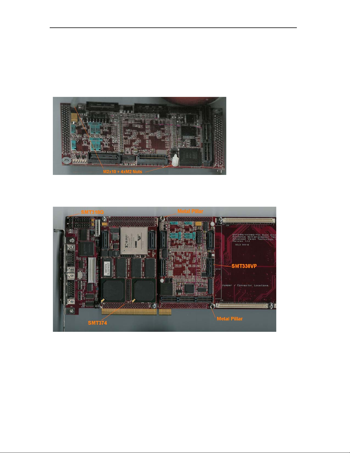
The example shown below is for an SMT8090_374 system
, which is a SMT374 and a
SMT390-VP on an SMT310Q carrier board.
The SMT390-VP is a combination of SMT338-VP and a SMT390.
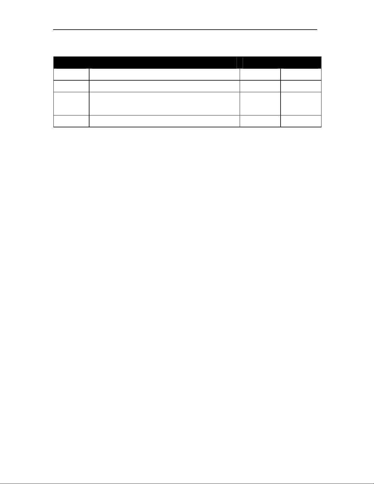
The following diagram shows both boards. The SMT390 has got 4 holes, as well as
the SMT338-VP, the usual two TIM mounting holes to provide the module with 3.3
Volts and two extra holes, smaller.
Top Primary TIM Connector
RSL
SHB
TIM 3.3V
Holes mounted with
Nylon screw (M2x10) and
4 Nylon nuts (M2)
B
B
SMT338-VP
RSL
SHB
Power
A
A
SMT390
Holes mounted with
Nylon screw (M2x10) and
4 Nylon nuts (M2)
Bottom Primary TIM Connector
TIM 3.3V
Figure 2 - SMT338-VP to SMT390 Interconnections.
Here is what is required to mount SMT338-VP+SMT390 on the SMT310Q:
Page 12
Version 1.3 Page 12 of 22 SMT338-VP User Manual
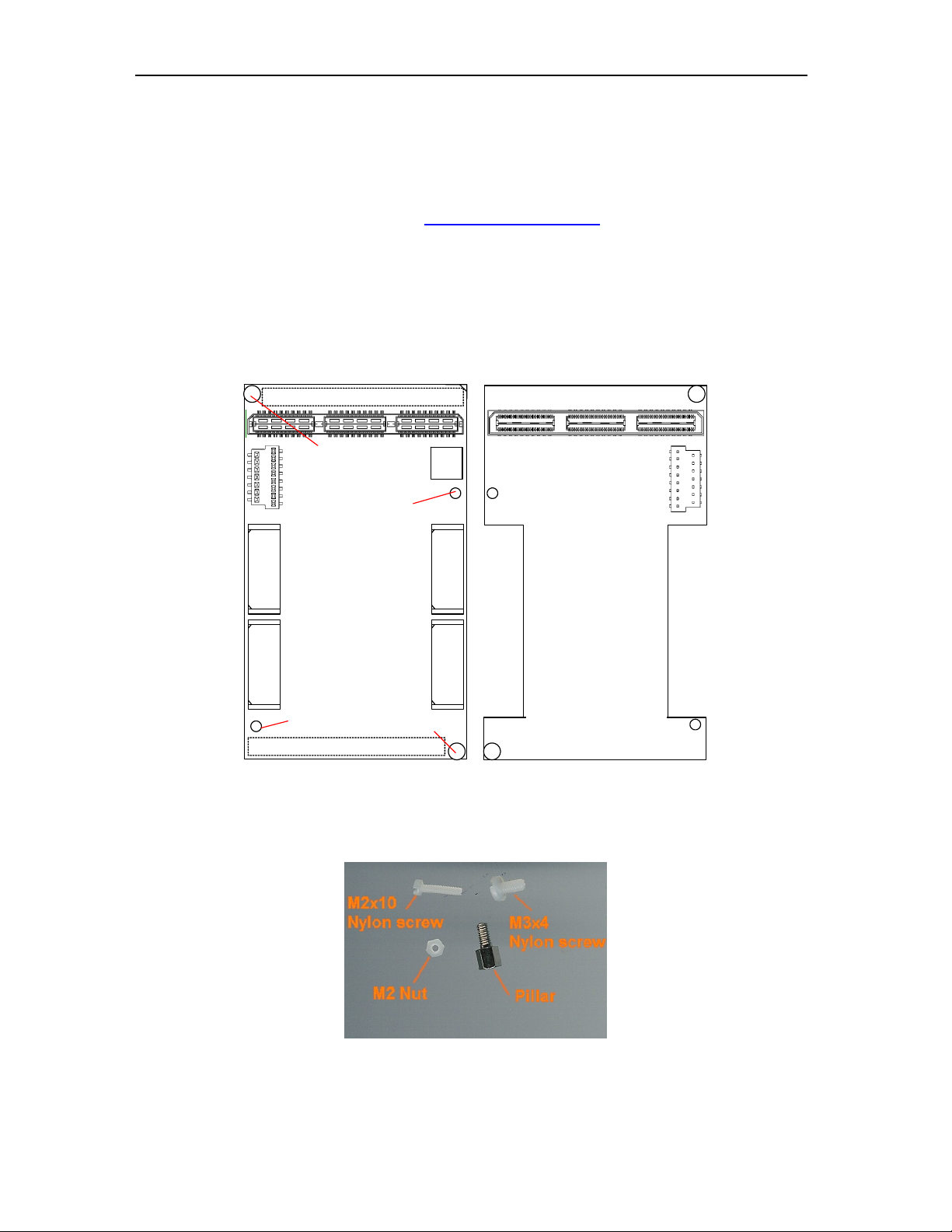
Figure 3 – Fixings
a – First, fit two Nylon screws (M2x10), pointing out (the head of the screws on
bottom side).
b – Then fit four M2 nuts on each screw.
c – Place the SMT338-VP on the second site (SMT374 already on first site) on
the SMT310Q and fit two metal pillars (3.3 Volts).
d – Place the SMT390 on top of the SMT338-VP. Make sure that both
modules fit firmly.
Page 13

Version 1.3 Page 13 of 22 SMT338-VP User Manual
e – Fit two M2 nuts on the Nylon screws and two M3x4 screws in the 3.3V
pillars.
Page 14

Functional description
This section describes in detail the implementation of the board.
Memory banks
Memory is organised in two independent banks.
Both banks can be accessed at the same time.
The following diagram shows how the DDR SDRAM components are organized
within a memory bank:
FPGA
32-bits data bus
16-bits data bus
DDR SDRAM
32 Meg x 16 bits
Chip Enable
16-bits data bus
DDR SDRAM
32 Meg x 16 bits
Figure 4: DDR SDRAM components bank organization
One bank is made from two 32M x 16-bits DDR SDRAM components
(
MT46V32M16FN), each of them having a 16-bit data bus. Memory components are
accessed in pairs.
Page 15

Version 1.3 Page 15 of 22 SMT338-VP User Manual
Oscillator
A 125 MHz low jitter oscillator is connected to the FPGA.
Connectors location
The following figure shows the location of connectors on SMT338-VP board.
Oscillator
LEDs
SLB
Figure 5: view of the top of SMT338-VP
RSL
SHBA
JTAG
SHBB RSL
Page 16

FPGA pinout
FPGA pinout is gathered in a Xilinx User Constraint File (ucf).
Naming convention is described below for SHB and SLB. Other signals are directly
commented in the UCF file itself.
SHB Pinout (LVTTL only)
The following provides naming convention for SHB signals.
2
n
i
P
1
n
i
P
e
n
a
l
p
d
n
u
o
r
G
l
a
r
g
e
t
n
I
0
.
5
m
m
d
a
l
B
a
e
B
d
n
a
e
m
n
g
i
s
e
D
g
i
l
A
n
i
P
t
n
e
m
n
Figure 6: Top view QSH 30
Page 17

Version 1.3 Page 17 of 22 SMT338-VP User Manual
UCF signal name Hw QSH Pin number QSH Pin number UCF signal name Hw
Shb?Hw0Clock
Shb?Hw0Data
Shb?Hw0Data
Shb?Hw0Data
Shb?Hw0Data
Shb?Hw0Data
Shb?Hw0Data
Hw0
Shb?Hw0Data
Shb?Hw0Data
Shb?Hw0Control(1)
Shb?Hw0Control(3)
Shb?Hw0Control(5)
Shb?FpgaIo(0)
Shb?FpgaIo(2)
Shb?FpgaIo(4)
Shb?FpgaIo(6)
Shb?FpgaIo(8)
Shb?FpgaIo(10)
Shb?Hw1Clock
Shb?Hw1Data
Shb?Hw1Data
Shb?Hw1Data
Shb?Hw1Data
Shb?Hw1Data
Shb?Hw1Data
Hw1
Shb?Hw1Data
Shb?Hw1Data
Shb?Hw1Control(1)
Shb?Hw1Control(3)
Shb?Hw1Control(5)
SHBxCLK0 1 2
SHBxD0(1) 3 4
SHBxD0(3) 5 6
SHBxD0(5) 7 8
SHBxD0(7) 9 10
SHBxD0(9) 11 12
SHBxD0(11) 13 14
SHBxD0(13) 15 16
SHBxD0(15) 17 18
SHBxUSER0(17) 19 20
SHBxUSER0(19) 21 22
SHBxREQ1 23 24
SHBxUSER1(23) 25 26
SHBxUSER1(25) 27 28
SHBxUSER1(27) 29 30
SHBxUSER1(29) 31 32
SHBxUSER1(31) 33 34
SHBxUSER1(33) 35 36
SHBxCLK3 37 38
SHBxD1(1) 39 40
SHBxD1(3) 41 42
SHBxD1(5) 43 44
SHBxD1(7) 45 46
SHBxD1(9) 47 48
SHBxD1(11) 49 50
SHBxD1(13) 51 52
SHBxD1(15) 53 54
SHBxUSER0(17) 55 56
SHBxUSER0(19) 57 58
SHBxREQ4 59 60
Shb?Hw0Data
Shb?Hw0Data
Shb?Hw0Data
Shb?Hw0Data
Shb?Hw0Data
Shb?Hw0Data
Shb?Hw0Data
Hw0
Shb?Hw0Data
Shb?Hw0Control(0)
Shb?Hw0Control(2)
Shb?Hw0Control(4)
Shb?Hw0Control(6)
Shb?FpgaIo(1)
Shb?FpgaIo(3)
Shb?FpgaIo(5)
Shb?FpgaIo(7)
Shb?FpgaIo(9)
Shb?FpgaIo(11)
Shb?Hw1Data
Shb?Hw1Data
Shb?Hw1Data
Shb?Hw1Data
Shb?Hw1Data
Shb?Hw1Data
Shb?Hw1Data
Hw1
Shb?Hw1Data
Shb?Hw1Control(0)
Shb?Hw1Control(2)
Shb?Hw1Control(4)
Shb?Hw1Control(6)
SHBxD0(0)
SHBxD0(2)
SHBxD0(4)
SHBxD0(6)
SHBxD0(8)
SHBxD0(10)
SHBxD0(12)
SHBxD0(14)
SHBxUSER0(16)
SHBxUSER0(18)
SHBxWEN1
SHBxACK1
SHBxUSER1(24)
SHBxUSER1(26)
SHBxUSER1(28)
SHBxUSER1(30)
SHBxUSER1(32)
SHBxUSER1(34)
SHBxD1(0)
SHBxD1(2)
SHBxD1(4)
SHBxD1(6)
SHBxD1(8)
SHBxD1(10)
SHBxD1(12)
SHBxD1(14)
SHBxUSER2(52)
SHBxUSER2(54)
SHBxWEN4
SHBxACK4
Page 18

Version 1.3 Page 18 of 22 SMT338-VP User Manual
Table 1: SHB interfaces table.
16-bit interface
Page 19

Version 1.3 Page 19 of 22 SMT338-VP User Manual
SLB pinout
The following diagram shows the SLB connector signals connected to the FPGA.
These names match with names available in UCF file.
Page 20

JTAG connector
The following 2 diagrams show connector J13 pinout.
1 2
3 4
5 6
7 8
9 10
11 12
13 14
Figure 7: J13 footprint
Figure 8: JTAG connector J13 pinout
Page 21

RSL
Follow is the RSL pinout.
RSL pin name refers to RSL pin-outs
documentation.
RSL type B:
RSL pin name FPGA pin number
TxLink0p A26
TxLink0n A27
RxLink0p A25
RxLink0n A24
TxLink1p A19
TxLink1n A20
RxLink1p A18
RxLink1n A17
TxLink2p A13
TxLink2n A14
RxLink2p A12
RxLink2n A11
TxLink3p A6
TxLink3n A7
RxLink3p A5
RxLink3n A4
Page 22

RSL type A:
RSL pin name FPGA pin number
TxLink0p AK6
TxLink0n AK7
RxLink0p AK5
RxLink0n AK4
TxLink1p AK13
TxLink1n AK14
RxLink1p AK12
RxLink1n AK11
TxLink2p AK19
TxLink2n AK20
RxLink2p AK18
RxLink2n AK17
TxLink3p AK26
TxLink3n AK27
RxLink3p AK25
RxLink3n AK24
 Loading...