

Page 1
Sundance Multiprocessor Technology Limited
User Manual
Unit / Module Description: VME64 carrier with 4 TIM sites
Unit / Module Number: SMT329
Document Issue Number:
Issue Date:
Original Author: S. E. Carpenter
User Manual
for
Form : QCF42
Date : 6 July 2006
SMT329
Sundance Multiprocessor Technology Ltd, Chiltern House, Waterside,
Chesham, Bucks. HP5 1PS.
This document is the property of Sundance and may not be copied nor
communicated to a third party without prior written permission.
© Sundance Multiprocessor Technology Limited 2006
User Manual SMT329 Last Edited: 09/02/2007 10:58:00
Page 2

Revision History
Issue Changes Made Date Initial
1.0 First draft 24th Jan 07 SEC
s
User Manual SMT329 Page 2 of 52 Last Edited: 09/02/2007 10:58:00
Page 3

Table of Contents
1 Introduction............................................................................................... 6
2 Related Documents .................................................................................... 7
2.1 Referenced Documents ..................................................................................................7
2.2 Applicable Documents....................................................................................................7
3 Acronyms, Abbreviations and Definitions..................................................8
3.1 Acronyms and Abbreviations.........................................................................................8
3.2 Definitions ......................................................................................................................8
4 Functional Description............................................................................. 10
4.1 Block Diagram ..............................................................................................................10
4.2 Module Description......................................................................................................10
4.2.1 Virtex 4......................................................................................................................11
4.2.2 Spartan 3..................................................................................................................13
4.2.3 CPLD .......................................................................................................................20
4.3 TIM Global Bus Resources...........................................................................................21
4.4 VME Interface...............................................................................................................22
4.4.1 VME slave interface to VME config and reset registers .........................................22
4.4.2 VME slave interface to the I/O registers.................................................................26
4.4.3 VME slave interface to the SRAM ...........................................................................27
4.4.4 TIM Global bus interface to the I/O registers ........................................................29
4.4.5 TIM Global bus interface to the VME bus master..................................................29
4.4.6 TIM Global bus interface to the SRAM.................................................................. 30
4.5 I/O Registers.................................................................................................................31
4.5.1 Comm Port Interface ...............................................................................................31
4.5.2 Reset (RST) register.................................................................................................34
4.5.3 Flash control interface.............................................................................................34
4.5.4 IO Control and Status registers...............................................................................36
4.6 Static RAM (sram).......................................................................................................40
4.7 JTAG Debugging Logic................................................................................................40
4.8 TIM Sites.......................................................................................................................41
4.8.1 TIM Connectors.......................................................................................................42
4.9 ROCKETIO....................................................................................................................42
4.10 Gigabit Ethernet ...........................................................................................................42
4.11 DMA controllers ...........................................................................................................43
4.12 Power Supplies .............................................................................................................43
4.13 Interface Description....................................................................................................44
4.13.1 Mechanical Interfac e ...............................................................................................44
User Manual SMT329 Page 3 of 52 Last Edited: 09/02/2007 10:58:00
Page 4

4.13.2 Electrical Interface...................................................................................................44
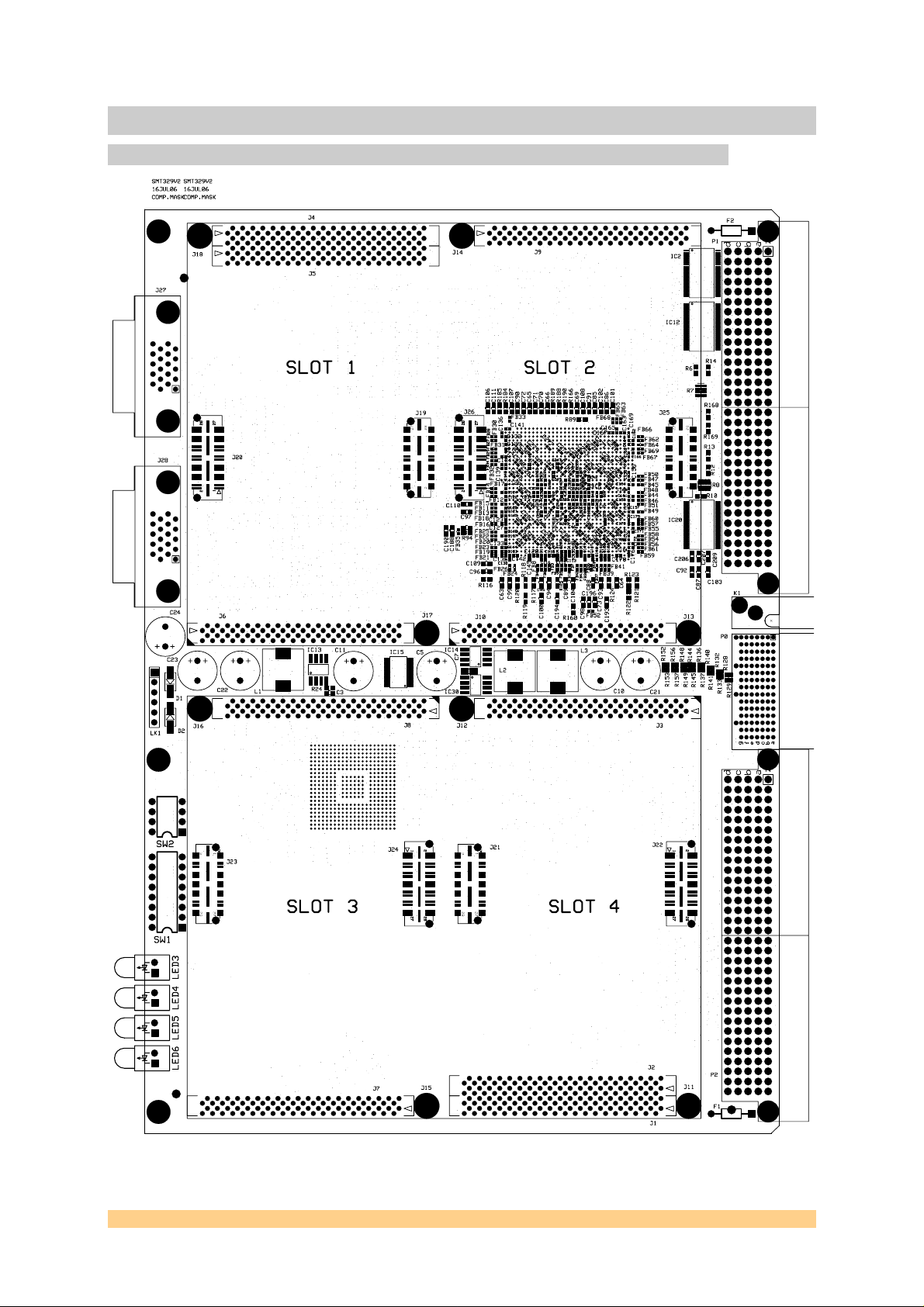
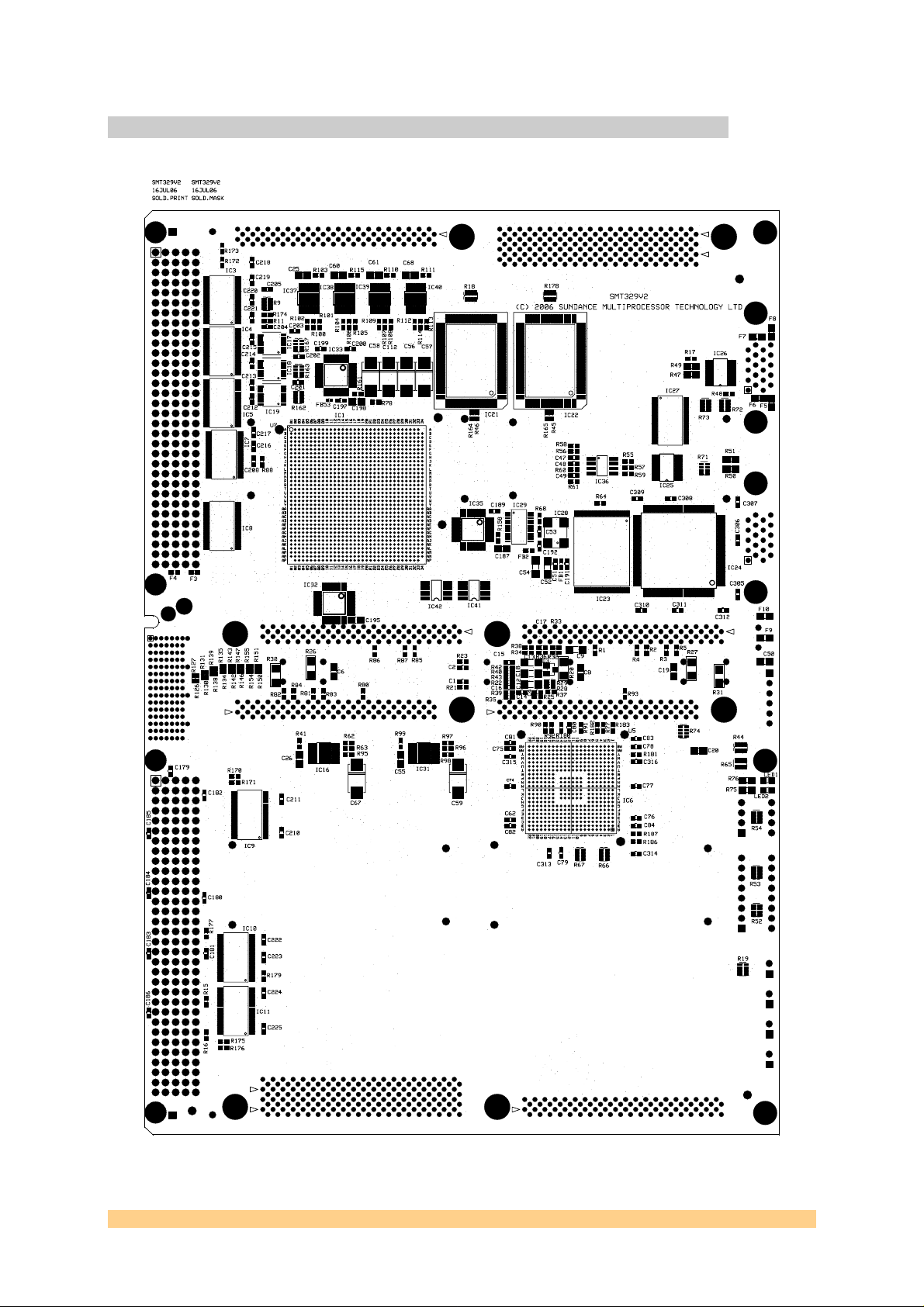
5 Footprint.................................................................................................. 45
5.1 Top View .......................................................................................................................45
5.2 Bottom View..................................................................................................................46
6 Pinout ...................................................................................................... 47
7 Support Packages..................................................................................... 52
8 Physical Properties .................................................................................. 52
9 Safety ....................................................................................................... 52
10 EMC ......................................................................................................... 52
User Manual SMT329 Page 4 of 52 Last Edited: 09/02/2007 10:58:00
Page 5

Table of Figures
Figure 1: SMT329 Architecture ..................................................................................................10
Figure 2: SMT329 Virtex4 internal bus architecture..................................................................11
User Manual SMT329 Page 5 of 52 Last Edited: 09/02/2007 10:58:00
Page 6

1 Introduction
The Smt329 is a VME four-site module carrier developed to provide ac cess to TIM Modules
over the VME64 (parallel) and VXS (serial) busses. It is backward compatible with the
SMT328, and can replace the SMT328 with no software mo difications. By implementing the
VME64 2eSST standard it offers up to 320M bytes/sec (2.56G bits/sec) across the VME bus,
while 8 VXS ports offer up to 2.5G bits/sec each, making a VXS total of up to 20G bits/sec.
The SMT329 has 8M bytes of high sp eed static ra m arranged as 1M by 64 bits, with a read or
write speed of at least 1G bytes/sec throughput for 64 bit transfers.
Buffered front panel JTAG ports allow control and debug of all 4 TIM modules
simultaneously, and multiple SMT329s.
All communications apart from JTAG and comms ports are controlled by a single Virtex 4
FPGA.
The 6 comms ports on each TIM (3 reset to out and 3 reset to in), and 2 comms ports on the
Virtex 4 (2 reset to out), are connected to a crossbar switch which allows a static
configuration to specify which of the 14 reset to out ports is connected to each of the 12 reset
to in ports. The switch is implemented in a Xilinx Spartan 3 FPGA. The switch topology is
stored in NVRAM and copied to the switch at board reset by the Virtex4.
The 2 RSL ports on each TIM are connected to Virtex4 Rocketio ports.
Four 1 Gigabit Ethernet ports are available on the VME P2 connector.
Two TIM sites have global bus interfaces to the Virtex4 for access to the static ram and VME
bus.
For use in legacy VME racks, SMT329 can be assembled with no P0 connector, and an on
board 3.3V PSU. It does not guarantee to support 2eVME or 2eSST and does not support
VXS, but it does retain the four Gigabit Ethernet ports on the P2 connector.
User Manual SMT329 Page 6 of 52 Last Edited: 09/02/2007 10:58:00
Page 7

2 Related Documents
2.1 Referenced Documents
SMT 328 User Guide 7p1
SMT329 Product Specification 20Dec05
2.2 Applicable Documents
TIM-40 Module Specification (1993)
ANSI/VITA 1.1-1997 American National Standard for VME64 Extensions
ANSI/VITA 1-1994 (R2002) American National Standard for VME64
2eSST ANSI/VITA 1.5-2003
VITA 41.0-200x VXS standard
SN74VMEH22501A data sheet Texas Instruments SCES620 – DECEMBER 2004
User Manual SMT329 Last Edited: 09/02/2007 10:58:00
Page 8

3 Acronyms, Abbreviations and Definitions
3.1 Acronyms and Abbreviations
C60
The terms C60, C64xx and TMS320C64xx are used interchangeably throughout this
document.
3.2 Definitions
Register Descriptions
The format of registers is described using diagrams of the following form:
31–24 23–16 15–8 7–0
LEVEL
R,00000000 RW,10000000 R,00000000 R,10000000
The digits at the top of the diagram indicate bit positions within the register and the central
section names bits or bit fields. The bottom row describes what may be done to the field and
its value after reset. Shaded fields are reserved and should only ever be written with zeroes.
R = Readable by the CPU
W = Writeable by the CPU
RW = Readable and writeable by the CPU
Binary digits indicate the value of the field after reset.
Byte Addressing
All byte addresses are “Big Endian”. This is defined as follows:
Decreasing numeric significance with increasing memory addresses.
So for the register definition shown above:
Bits 31-24 = Byte Address 0
Bits 23-16 = Byte Address 1
Bits 15-8 = Byte Address 2
Bits 7-0 = Byte Address 3
Care must be taken when using an Intel (PC) little endian based VME host controller, to
ensure the use of either hardware or software byte swapping when accessing the SMT329
over the VME bus.
VME64 and legacy VME systems
A VME64 system meets the ANSI/VITA specification for VME64, with 160 pin backplane
connectors and a 3.3 Volt backplane supply.
User Manual SMT329 Last Edited: 09/02/2007 10:58:00
Page 9

A “legacy” VME system meets the ANSI/VITA specification for VME, with 96 pin
backplane connectors and NO 3.3 Volt backplane supply.
The SMT329 is always fitted with 160 pin connectors, which are designed to successfully
mate with either a VME64 system or a legacy VME system.
User Manual SMT329 Page 9 of 52 Last Edited: 09/02/2007 10:58:00
Page 10
4 Functional Description
4.1 Block Diagram
Figure 1: SMT329 Architecture
4.2 Module Description
Figure 1 shows the SMT329 block diagram. There are 4 single width or 2 double width TIM
sites. All communications apart from the comms port switching are routed through the Xilinx
Virtex4 fpga, including all VME and SRAM i/o. Comms port cross bar switching is
performed by a Xilinx Spartan3. Loading the configuration data into the 2 fpgas and
managing the JTAG interface are performed by a Xilinx CPLD.
User Manual SMT329 Last Edited: 09/02/2007 10:58:00
Page 11
4.2.1 Virtex 4
Figure 2: SMT329 Virtex4 internal bus architecture
Figure 2 shows the SMT329 bus architecture within the Virtex4. This is backwards
compatible with SMT328, with the addition of a 4 channel Ethernet DMA engine, a 4 channel
Rocketio DMA engine, and a Rocketio cross bar switch matrix.
User Manual SMT329 Page 11 of 52 Last Edited: 09/02/2007 10:58:00
Page 12

Table 1 below shows the actual implementation of the parall el bus connectivity for the VME
slave, TIM global 1, TIM global 2, DMAA, DMAB. These 5 separate bus masters each have
fully dedicated connections to an arbitrating bus switch, which can con nect all 5 masters to
any 5 slaves out of the 8 available, AT THE SAME TIME. This architecture avoids the
traditional bottle neck problems associated with a single bus, which is used by on e master at
a time.
Slave S1 S2 S3 S4 S5 S6 S7 S8
Master VME&
Reset
Control
& DMA
Flash Sram VME
Master
Comms RSLA RSLB
M1 VME
Y Y Y Y N Y Y Y
Slave
M2 TIM
N Y Y Y Y N Y Y
Global1
M3 TIM
N Y Y Y Y N Y Y
Global2
M4 DMAA
N N N Y Y N Y Y
M5 DMAB
N N N Y Y N Y Y
Table 1: SMT329 Virtex4 internal bus architecture
There are exceptions to the permitted connectivity indic ated by “Y” for connection p ermitted
and “N” for no connection.
Revision 1 of the Virtex 4 configuration, provides functional equivalence with the SMT328,
which it replaces. Subsequent releases of the Virtex 4 configuration will provide support for
the following additional functions:
VME64 burst transfer modes.
VME 2eSST transfer modes.
RSL TIM interfaces.
1G bit Ethernet connectivity.
DMA to and from the SRAM.
VXS connectivity.
Subsequent revisions of the Virtex 4 configuration will be mad e available on the Sundance
WEB site along with a utility for updating their flash images on the SMT329. Updates to this
manual will accompany new firmware releases.
User Manual SMT329 Page 12 of 52 Last Edited: 09/02/2007 10:58:00
Page 13

4.2.2 Spartan 3
The SMT329 comms port mapping is performed by a cross bar switch implemented in a
Xilinx Spartan3 fpga. The cross bar switch has 12 Reset To In (RTI) ports and 14 Reset To
Out (RTO) ports.
Table 2 below illustrates the architecture:
RTI 0 1 2 3 4 5 6 7 8 9 10 11
RTO T1C3 T1C4 T1C5 T2C3 T2C4 T2C5 T3C3 T3C4 T3C5 T4C3 T4C4 T4C5
0 T1C0 Y Y Y Y Y Y Y Y Y Y Y Y
1 T1C1 Y Y Y Y Y Y Y Y Y Y Y Y
2 T1C2 Y Y Y Y Y Y Y Y Y Y Y Y
3 T2C0 Y Y Y Y Y Y Y Y Y Y Y Y
4 T2C1 Y Y Y Y Y Y Y Y Y Y Y Y
5 T2C2 Y Y Y Y Y Y Y Y Y Y Y Y
6 T3C0 Y Y Y Y Y Y Y Y Y Y Y Y
7 T3C1 Y Y Y Y Y Y Y Y Y Y Y Y
8 T3C2 Y Y Y Y Y Y Y Y Y Y Y Y
9 T4C0 Y Y Y Y Y Y Y Y Y Y Y Y
10 T4C1 Y Y Y Y Y Y Y Y Y Y Y Y
11 T4C2 Y Y Y Y Y Y Y Y Y Y Y Y
12 VXC1 Y Y Y Y Y Y Y Y Y Y Y Y
13 VXC2 Y Y Y Y Y Y Y Y Y Y Y Y
Table 2: SMT329 Spartan 3 comms port switch internal architecture
This switch has no connectivity restrictions.
The connectivity map is loaded by the CPLD directly from flash memory following power on,
after the Spartan 3 configuration is loaded, but before the Virtex 4 configuration is loaded.
This connectivity map can be changed by the user, who uses a flash program ming utility to
write a new map into the flash. This map is then loaded into the Spartan 3 the next time the
SMT329 is powered on.
4.2.2.1 Comms Switch Map
The map has 12 entries, each of which defines which RTI is connected to which RTO. So entry
1 defines which RTO is connected to RTI 1, and entry 12 defines which RTO is connected to
RTI 12. Each entry has a value in the range 0 to 13 as there are 14 RTO ports. Each entry must
be different.
User Manual SMT329 Page 13 of 52 Last Edited: 09/02/2007 10:58:00
Page 14

The map itself is embedded in a normal text file, and the whole text file is stored in the flash,
so that the map can be accompanied by any descriptive text, up to a maximum file size of 64K
bytes. The map is identified in the text by the keyword “SMT329MAP
The SMT329 flash can be programmed from ei ther the VME bus or by a TIM in either slot 1
or 4. The map is loaded from the flash into th e Sp artan3 fpga by the CPLD, immediately after
the SMT329 power is stable following switch on. The map can not be loaded at any other
time. The map must load without error for the cross bar switch to work correctly. The
Spartan3 performs the following data validation checks before enabling the switch:
1. All entries are in the range 0 to 13.
2. No entry is the same.
If either of these criteria are not met, the switch will not be enabled.
”.
4.2.2.2 Comms Switch Map port connectivity
The 12 RTI ports and 14 RTO ports are connected as follows:
Switch port RTI port RTO port
0 T1C3 T1C0
1 T1C4 T1C1
2 T1C5 T1C2
3 T2C3 T2C0
4 T2C4 T2C1
5 T2C5 T2C2
6 T3C3 T3C0
7 T3C4 T3C1
8 T3C5 T3C2
9 T4C3 T4C0
10 (0xA) T4C4 T4C1
11 (0xB) T4C5 T4C2
12 (0xC) not connected VXC1 (VME port 1)
13 (0xD) not connected VXC2 (VME port 2)
4.2.2.3 Comms Switch Map Example 1
User Manual SMT329 Page 14 of 52 Last Edited: 09/02/2007 10:58:00
Page 15

This example duplicates the default connectivity of th e SMT328, and is loaded in the flash
during SMT329 production, filename “s329map.txt” :
SMT329MAPCAB012345D78
SUNDANCE SMT329 STANDARD COMMS PORT MAP MIMICS SMT328
DATE: 17-DEC-06
COMPANY: SUNDANCE
AUTHOR: SEC
Connect SMT329 to mimic a standard SMT328
Entry Value Description
1 12 = 0xC T1C3 (RTI) to VXC1 (RTO)
2 10 = 0xA T1C4 (RTI) to T4C1 (RTO)
3 11 = 0xB T1C5 (RTI) to T4C2 (RTO)
4 0 = 0x0 T2C3 (RTI) to T1C0 (RTO)
5 1 = 0x1 T2C4 (RTI) to T1C1 (RTO)
6 2 = 0x2 T2C5 (RTI) to T1C2 (RTO)
7 3 = 0x3 T3C3 (RTI) to T2C0 (RTO)
8 4 = 0x4 T3C4 (RTI) to T2C1 (RTO)
9 5 = 0x5 T3C5 (RTI) to T2C2 (RTO)
10 13 = 0xD T4C3 (RTI) to VXC2 (RTO)
11 7 = 0x7 T4C4 (RTI) to T3C1 (RTO)
12 8 = 0x8 T4C5 (RTI) to T3C2 (RTO)
The map file is stored in the flash in ascii
and has a keyword identifier immediately before the map data of
"SMT329MAP"
This is the map which is duplicated at the top of the file:
SMT329MAPCAB012345D78
-END-
The very first line begins with the map keyword “SMT329MAP“, although it can appear
anywhere in the text. This is immediately followed by “CAB012345D78” which is the actual
map. The descriptive text which follows explains each map entry.
4.2.2.4 Comms Switch Map Example 2
User Manual SMT329 Page 15 of 52 Last Edited: 09/02/2007 10:58:00
Page 16

This example is used for testing, and with the correct TIM software implements a spiral
which allows loop back testing of all ports on all tims at once. Filename
“S329MAPSPIRAL1.txt” :
SMT329MAPCAB012345678
SUNDANCE SMT329 SPIRAL1 TEST COMMS PORT MAP
This map implements a spiral connection of comms ports to
allow testing all comms ports from VME port 1.
It can not test VME port 2.
DATE: 17-DEC-06
COMPANY: SUNDANCE
AUTHOR: SEC
This is the 328 equivalent map:
Entry Value Description
1 12 = 0xC T1C3 (RTI) to VXC1 (RTO)
2 10 = 0xA T1C4 (RTI) to T4C1 (RTO)
3 11 = 0xB T1C5 (RTI) to T4C2 (RTO)
4 0 = 0x0 T2C3 (RTI) to T1C0 (RTO)
5 1 = 0x1 T2C4 (RTI) to T1C1 (RTO)
6 2 = 0x2 T2C5 (RTI) to T1C2 (RTO)
7 3 = 0x3 T3C3 (RTI) to T2C0 (RTO)
8 4 = 0x4 T3C4 (RTI) to T2C1 (RTO)
9 5 = 0x5 T3C5 (RTI) to T2C2 (RTO)
10 13 = 0xD T4C3 (RTI) to VXC2 (RTO)
11 7 = 0x7 T4C4 (RTI) to T3C1 (RTO)
12 8 = 0x8 T4C5 (RTI) to T3C2 (RTO)
This is the sprial test map:
Entry Value Description
1 12 = 0xC T1C3 (RTI) to VXC1 (RTO)
2 10 = 0xA T1C4 (RTI) to T4C1 (RTO)
3 11 = 0xB T1C5 (RTI) to T4C2 (RTO)
4 0 = 0x0 T2C3 (RTI) to T1C0 (RTO)
5 1 = 0x1 T2C4 (RTI) to T1C1 (RTO)
6 2 = 0x2 T2C5 (RTI) to T1C2 (RTO)
7 3 = 0x3 T3C3 (RTI) to T2C0 (RTO)
8 4 = 0x4 T3C4 (RTI) to T2C1 (RTO)
9 5 = 0x5 T3C5 (RTI) to T2C2 (RTO)
10 6 = 0x6 T4C3 (RTI) to T3C0 (RTO)
11 7 = 0x7 T4C4 (RTI) to T3C1 (RTO)
12 8 = 0x8 T4C5 (RTI) to T3C2 (RTO)
It assumes the following software routing in the TIMs:
User Manual SMT329 Page 16 of 52 Last Edited: 09/02/2007 10:58:00
Page 17

TIM1-3:
C3=>C0
C4=>C1
C5=>C2
TIM4:
C3=>C1
C4=>C2
C5=>C5 (loop back)
The map file is stored in the flash in ascii
and has a keyword identifier immediately before the map data of "SMT329MAP"
This is the map which is duplicated at the top of the file:
SMT329MAPCAB012345678
-END-
The very first line begins with the map keyword “SMT329MAP“, although it can appear
anywhere in the text. This is immediately followed by “
CAB012345678” which is the actual
map. The descriptive text which follows explains each map entry.
4.2.2.5 Comms Switch Map Programming
The map text file can be programmed from either the VME or from TIM slot 1 or slot 4. The
VME controller map write program is written for a Xycom XVME-660 PC host running DOS,
and will need porting to any other environment. The TIM map write program is written for
an SMT395, but will also run on an SMT365 and some other TIMs, unchanged.
The source code for both programs is available for information only. Extreme care is required
if these programs are modified, as damage to the other contents of the SMT329 flash may
result in complete failure of the board, as the flash also contains the configuration i mages for
both the Spartan3 and the Virtex4.
Note that the red front panel LED is on, and the VME bus signal SYSFAIL is driven low, when
the Virtex4 has not been configured. This state will continue indefinitely if the flash is
corrupted, but should normally only be seen briefly immediately after switch on.
In order to provide user protection from flash corruption, 2 separate security features are
implemented, in addition to the write sequence security built into the flash device:
1. A 32 bit KEY register must be loaded with the flash write key to enable writes to the flash.
2. The flash has been divided into a factory and a user area . The user flas h programming tool
only writes to the user area, the factory area remains unchanged. This means that it should
always be possible to set the SMT329 to the standard map (example 1) by switching to the
factory flash area. The flash area used by the CPLD after power on, is controlled by the DIP
switch SW2 bit 4 as follows:
SW2/4 OFF = Factory area (UVB4 = 1)
SW2/4 ON = User area (UVB4 = 0)
User Manual SMT329 Page 17 of 52 Last Edited: 09/02/2007 10:58:00
Page 18

4.2.2.6 Comms Switch Map Diagnostic Port and Error Detection
An 8 bit diagnostic read only port is provided by the Spartan3. This port operates by setting
an 8 bit register address, then reading the 8 bit register value. The following registers are
currently defined:
Register
address
00 Map entry 0 + 0x80 if transmitting
01 Map entry 1 + 0x80 if transmitting
02 Map entry 2 + 0x80 if transmitting
03 Map entry 3 + 0x80 if transmitting
04 Map entry 4 + 0x80 if transmitting
05 Map entry 5 + 0x80 if transmitting
06 Map entry 6 + 0x80 if transmitting
07 Map entry 7 + 0x80 if transmitting
08 Map entry 8 + 0x80 if transmitting
09 Map entry 9 + 0x80 if transmitting
0A Map entry A + 0x80 if transmitting
0B Map entry B + 0x80 if transmitting
0C 0x0C
0D 0x0D
Description
0E 0x0E
0F 0x0F
10 RTO 0 is connected to this RTI + 0x80 if transmitting
11 RTO 1 is connected to this RTI + 0x80 if transmitting
12 RTO 2 is connected to this RTI + 0x80 if transmitting
13 RTO 3 is connected to this RTI + 0x80 if transmitting
14 RTO 4 is connected to this RTI + 0x80 if transmitting
15 RTO 5 is connected to this RTI + 0x80 if transmitting
16 RTO 6 is connected to this RTI + 0x80 if transmitting
17 RTO 7 is connected to this RTI + 0x80 if transmitting
18 RTO 8 is connected to this RTI + 0x80 if transmitting
19 RTO 9 is connected to this RTI + 0x80 if transmitting
User Manual SMT329 Page 18 of 52 Last Edited: 09/02/2007 10:58:00
Page 19

1A RTO A is connected to this RTI + 0x80 if transmitting
1B RTO B is connected to this RTI + 0x80 if transmitting
1C RTO C (VXC1) is connected to this RTI + 0x80 if transmitting
1D RTO D (VXC2) is connected to this RTI + 0x80 if transmitting
1E 0X1E
1F 0X1F
20 Error map 0
21 Error map 1
22 Spartan3 FPGA revision MSB
23 Spartan3 FPGA revision LSB
24 to FF <returns the register address>
The error maps are bit maps which have an error bit for each map entry:
Error map 0 has error bits for map entry 7 to 0
Error map 1 has bits 7-4 set to 0, then error bits for map entry 0xB to 8.
Both error maps must be 0 for the switch to be enabled.
The register address is set and the register value read from a single byte address.
Both the VME bus controller and either TIM1 or TIM4 can access it at these addresses:
VME I/O space address offset = 0xDF
TIM I/O space address = 0xC0000102
User Manual SMT329 Page 19 of 52 Last Edited: 09/02/2007 10:58:00
Page 20

4.2.3 CPLD
The CPLD performs 3 primary functions: It loads the fpga configurations and comms port
switch map from flash, immediately after power on. It also manages the JTAG switching
required to maintain an intact serial data stream with any number of TIM slots occupied. It
also controls the low level board reset.
The flash is divided into a user area and a factory area. An SMT329 is shipped with both
these areas containing a Spartan 3 configuration, a standard comms port map, and a Virtex 4
configuration. The user can choose which area is us ed by the CPLD to load from, by setting
DIP switch SW2 bit 4 as follows:
SW2/4 OFF = Factory area (UVB4 = 1)
SW2/4 ON = User area (UVB4 = 0)
If the CPLD fails to configure an FPGA using the user area data, it will then try loading from
the factory area.
User Manual SMT329 Page 20 of 52 Last Edited: 09/02/2007 10:58:00
Page 21

4.3 TIM Global Bus Resources
There are three main global bus resources availa ble to TIMs on this motherboard. These are
the 32 bit VME bus, the 8 Megabyte static ram (sram), and the board control registers.
The VME bus is directly accessible to the TIMs without reducing the availability of the sram
to any other internal sram requestor.
The TIMs can access the sram with zero wait states for burst transfers, after ar bitration for
the sram bus.
Access to the global resources is selected by an arbitration state machine. Resources remain
granted to the last resource master after the cycle has finished so that contiguous transfer s
proceed without further arbitration. Arbitration only occurs when two (or more) possible bus
masters are requesting the same resource.
Because the TIMs have direct access to the VME bus, the risk of dead lock that was present i n
the SMT328 is now removed. This is because the VME bus arbiter, on another VME bus
board, is the only arbiter in the path to granting bus master acc ess to the VME bus for the
TIM, whereas on SMT328 the VME bus arbiter and the sram bus arbiter bo th had to grant
access.
User Manual SMT329 Page 21 of 52 Last Edited: 09/02/2007 10:58:00
Page 22
4.4 VME Interface
The VME interface uses the P1 connector and the center row (B) of the P2 connector for
additional data and address lines. The interface forms a complete D8/16/32/64 master/slave.
The SMT329 does not support slot 0 operation or unaligned transfers.
Rows A and C of the P2 connector are connected to 4 of the Virtex4 RSL transmit receive
pairs. This allows the fitting of a rear transition PCB to support external high speed serial
interfaces such as 1M bit Ethernet, on both VME64 and legacy VME systems.
A central P0 connector is a factory fitted option which allows connection to a back plane
which supports the VXS standard. The P0 connector has 4 fixed RSL transmit receive pairs.
The VME64 bus is buffered with SN74VMEH22501A transceivers from TI which are s pecially
designed to be compliant with VME64, 2eVME protocols in VME64x (ANSI/VITA 1.1) and
2eSST protocols in VITA 1.5. With proper design of a 21-slot VME64 system, a designer can
achieve 320-Mbyte transfer rates on linear backplanes and, possibly up to 1-Gbyte/sec
transfer rates on the VME320 backplane.
For legacy VME systems without a 3.3 Volt supply, SMT329 can be assembled with an on
board 3.3V PSU. In a legacy VME system the SMT329 does not guarantee to support 2eVME
or 2eSST and does not support VXS, but it does retain the four Gigabit Ethernet ports on the
P2 connector.
The use of high speed transfer modes (2eVME and 2eSST) on legacy backplan es VME is not
supported, and may or may not function reliably.
The VME master interface can be used by eith er TIM1 or TIM4 g lobal bus, and by D MAA and
DMAB.
The SMT329 VME slave interface allows direct access by the current VME bus master to 7 out
of the 8 available SMT329 slaves, as shown in table 1 above. It has 3 separately decoded VME
bus address spaces, divided as follows:
Name VME
space
VME
configuration
I/O A32 256 Comm-port, Board Reset, Control, Flash
I/O2 A32 768 DMA, RSL
SRAM A32 8M Static Ram
The A16 VME configuration base address is set with an 8 way DIP switch labelled SW1. This
sets the value to compare to VME A6-A13, with VME A14-A15 always compared to 1 in order
to generate a board decode. This A16 address space contains board identification registers
and a pair of 16 bit registers which must be loaded with the base address of the I/O and
SRAM spaces.
A16 64 Identification and programmable base addresses
Size in
Bytes
Description
for I/O and SRAM. Board Reset.
4.4.1 VME slave interface to VME config and reset registers
User Manual SMT329 Page 22 of 52 Last Edited: 09/02/2007 10:58:00
Page 23
These registers are decoded in the VME A16 space, which means that the VME address
modifiers must be set to either of the following:
Hex Code VME
Function
space
2D A16 Short supervisory access
29 A16 Short non privileged access
The VME address bits are decoded as follows:
VME Address
Compare to Comment
bit
15 1 Must be high
14 1 Must be high
13 SW1/1 On = 0 Off = 1
12 SW1/2 On = 0 Off = 1
11 SW1/3 On = 0 Off = 1
10 SW1/4 On = 0 Off = 1
9 SW1/5 On = 0 Off = 1
8 SW1/6 On = 0 Off = 1
7 SW1/7 On = 0 Off = 1
6 SW1/8 On = 0 Off = 1
5-1 - Select individual registers
Note that VME address bits A16 and above are ignored.
Example: SW1 switches 1-7 set to off, switch 8 set to on gives a VME A16 base address of
0xff80.
VME address bits 5 and below decode the following 16 bit wide registers:
Offset (hex) Register
00-01 Board ID
02-03 Device type
04-05 Status / Control
06-07 SRAM base address
08-09 I/O base address
0A-3B Unused
User Manual SMT329 Page 23 of 52 Last Edited: 09/02/2007 10:58:00
Page 24

3C-3D Virtex4 code revision
3E-3F Manufacturer ID
4.4.1.1 VME Board ID Register (address 00-01)
The bit definitions for this register are:
15–12 11–0
ID1 ID2
R, 0101 R, 0000 0111 1011
Always reads as 507B hex.
4.4.1.2 VME Device Type Register (address 02-03)
The bit definitions for this register are:
15–12 11–0
Memory Size 8 Model Code 329
R, 1000 R, 0001 0100 1001
Memory size is defined as the number of significant bits in an A32 address used to specify the
sram base address.
So this register reads as: 0x8149
4.4.1.3 VME Master Status and Control Register (address 04-05)
The bit definitions for the VME Master Status and Control register are:
15 14-4 3 2-1 0
A32 Enabled
RW, 0 R,000 0000 0001 R, x R, 10 RW, 0
Bit 15 is cleared by a board reset so that the A32 base address registers can be initialised
before A32 enable is set. A32 enable MUST be set to allow A32 access to the rest of the board.
Ready Reset board
If this bit is clear (0) then no A32 access will be decoded and a bus error will
occur for all A32 read/write cycles.
It is very strongly recommended that all VME bus cycles have some form of BUS_ERROR
checking enabled, as it is an essential error reporting feature which should not be ignored.
User Manual SMT329 Page 24 of 52 Last Edited: 09/02/2007 10:58:00
Page 25

Note that a VME bus error is generated by the VME slot 0 controller after a timeout period,
not by the SMT329.
The SMT329 can be reset at any time by the VM E controller setting bit 0. As this bit is itself
cleared by a board reset, it will always read as 0.
The Ready bit is driven by the TIM config signal which indicates when all TIMs are ready
following a reset.
4.4.1.4 VME Sram Base Address Register (address 06-07)
This 16-bit register defines the base address of the sram for A32 addressing modes. The most
significant 9 bits of this register (D15-7) are compared to VME address signals A31-23. VME
address signals A22-A1 decode bytes in the 8M byte SRAM. The least significant 7 bits of this
register are not used.
4.4.1.5 VME I/O Base Address Register (address 08-09)
This 16-bit register is used to set the base address (in 256 byte blocks) of the I/O address
space.
This 16 bit base address is compared to the incoming A32 address bits A23-8, while bits A3124 are compared to FF hex. A match decodes a 256 byte sp ace which is further decoded to
access the various devices in the I/O address space.
The 256 byte space is functionally equivalent to the I/O space in the SMT328 . This space can
be expanded in the SMT329 by 768 bytes to a total size of 1024 bytes. This expansion is
software enabled, to maintain backwards compatibility. When the full 1024 byte space is
enabled, bits 0 and 1 of this VME I/O base address register are ignored.
4.4.1.6 VME Virtex 4 code revision
This 16 bit read only register reports the current revision of Virtex4 FPGA code.
4.4.1.7 VME Sub-class Register (1E)
The bit definitions for this 16-bit read only register are given below:
The bit definitions for this register are:
15 14-12 11-0
Sub class ID3
R, 0 R, 001 R, 0000 0111 1011
Always reads as 107B hex.
User Manual SMT329 Page 25 of 52 Last Edited: 09/02/2007 10:58:00
Page 26
4.4.2 VME slave interface to the I/O registers
This I/O address space occupies 256 bytes for the basic I/O functions, and a further 768 byte
I/O2 space can be software enabled, to provide VME access to the expanded functions such
as DMA and RSL interfaces.
The I/O space has a base address set by the VME controller in the VME configuration regist er
“I/O Offset Register”.
This address space is decoded in the VME A32 space, which means that the VME address
modifiers must be set to either of the following:
Hex Code VME
Function
space
0D A32 Extended supervisory data access
09 A32 Extended non privileged data access
The VME address bits are decoded as follows for the basic 256 byte I/O space:
VME
Compare to Comment
Address
bit
31-24 1 Must be high
23-8 I/O Base D15-0 16 bit I/O Base programmed by the VME controller
7-1 - Select individual registers in 256 byte space
The VME address bits are decoded as follows for the full 1024 byte I/O space:
VME
Compare to Comment
Address
bit
31-24 1 Must be high
23-10 I/O Base D15-2 14 bit I/O Base programmed by the VME controller
9-1 - Select individual registers in 1024 byte space
User Manual SMT329 Page 26 of 52 Last Edited: 09/02/2007 10:58:00
Page 27

Individual I/O register addresses are detailed in the following table:
Area VME offset TIM address Peripheral Read/Write
Reserved 00-7C None - -
COMM 80-83 None Comm-port data Read/write
COMM 84-87 None Comm-port data Read/write
COMM 88-8C None
COMM 90-93 None Comm-port
Read/write
status
COMM 94-BC None
RST C0-C3 None Reset board Read/Write
RST C4-CC None
FLASH D0-D3 C000 0100 Flash data Read/Write
FLASH D4-D7 C000 0101 Flash address Read/Write
FLASH D8-DB C000 0102 Flash Key Read/Write
FLASH DC-DF C000 0103 SP3 diagnostic Read/Write
CONTROL E0-E3 C000 0000 Control 1 Read/Write
CONTROL E4-E7 C000 0001 Control 2 Read/Write
CONTROL E8-EB C000 0002 Control 3 Read/Write
CONTROL EC-EF C000 0003 Control 4 Read/Write
CONTROL F0-F3 C000 0004 Status 1 Read
CONTROL F4-F7 C000 0005 Control 6 Read/Write
CONTROL F8-FB C000 0006 Control 7 Read/Write
CONTROL FC-FF C000 0007 Reserved -
I/O2 100-3FF C000 0200-
DMA & RSL Read/Write
C000 02FF
Note that I/O2 must be software enabled to be available to the VME bus. When it is disabl ed,
the SMT329 will not respond to addre sses in this area, and a VME bus error will result.
Actual DMA and RSL addresses in the IO2 space will be defined in a subsequent release of
this manual and Virtex4 configuration.
4.4.3 VME slave interface to the SRAM
User Manual SMT329 Page 27 of 52 Last Edited: 09/02/2007 10:58:00
Page 28

The sram is organised to allow the VME bus master to perform D8, D16, D32 or D64 cycles,
and word swapping buffers are included for this purpose. Transfers can be single, or burst
using either 2eVME or 2eSSTT. This address space occupies 8M bytes, and has a base
address set by the VME controller in the VME configuration register “SRAM Base Address”.
This address space is decoded in the VME A32 space, which means that the VME address
modifiers must be set to either of the following:
Hex Code VME
Function
space
0D A32 Extended supervisory data access
09 A32 Extended non privileged data access
The VME address bits are decoded as follows:
VME Address
Compare to Comment
bit
31-23 SRAM Base
SRAM Base is programmed by the VME controller
D15-7
22-0 - Select byte address in the 8M byte SRAM
The VME interface to the SRAM supports byte write.
User Manual SMT329 Page 28 of 52 Last Edited: 09/02/2007 10:58:00
Page 29
4.4.4 TIM Global bus interface to the I/O registers
This address space occupies global bus addresses in the following region:
0xC000 0000 to 0xC0FF FFFF.
Individual I/O register addresses are detailed in the following table:
Area VME offset TIM address Peripheral Read/Write
FLASH D0-D3 C000 0100 Flash data Read/Write
FLASH D4-D7 C000 0101 Flash address Read/Write
FLASH D8-DB C000 0102 Flash Key Read/Write
FLASH DC-DF C000 0103 SP3 diagnostic Read/Write
CONTROL E0-E3 C000 0000 Control 1 Read/Write
CONTROL E4-E7 C000 0001 Control 2 Read/Write
CONTROL E8-EB C000 0002 Control 3 Read/Write
CONTROL EC-EF C000 0003 Control 4 Read/Write
CONTROL F0-F3 C000 0004 Status 1 Read
CONTROL F4-F7 C000 0005 Control 6 Read/Write
CONTROL F8-FB C000 0006 Control 7 Read/Write
CONTROL FC-FF C000 0007 Reserved -
I/O2 100-3FF C000 0200-
DMA & RSL Read/Write
C000 02FF
Actual DMA and RSL addresses in the IO2 space will be defined in a subsequent release of
this manual and Virtex4 configuration.
4.4.5 TIM Global bus interface to the VME bus master
This address space occupies global bus addresses in the following region:
0xC100 0000 to 0xC13F FFFF.
A global bus cycle in this address space causes a corresponding VME bus cycle. The VME
master takes the global bus address and shifts it left 2 bits to create a byte address. Bits 23-2
of this byte address are mapped directly to the VME bus address. It then takes the 8 bit VME
high address in Control register 4 to generate VME address bits 31-24, and the VME A1 bit in
Control register 4 is mapped to VME bus address A1. The following table details this process:
User Manual SMT329 Page 29 of 52 Last Edited: 09/02/2007 10:58:00
Page 30

VME
address
bit
Global
address
bit
Control 4
register
bit
Description
31-24 - 31-24 High 8 bits
23-2 21-0 - Middle 22 bits
1 - 16 A1
0 - 17 A0 / -Lword
The VME address modifiers, DS0 and DS1 are copied directly from control register 4. The
VME bus request level is also specified in control register4.
So a TIM can directly address 16M bytes in the VME bus address space.
Note that the TIM global bus does not support byte addressi ng, so transfers to and from the
VME bus are always 32 bits wide.
4.4.6 TIM Global bus interface to the SRAM
This address space occupies global bus addresses in the following region:
0xDFE0 0000 to 0xDFFF FFFF.
This space occupies 2M 32 bit words or 8M bytes.
Note that the TIM global bus does not support byte addressi ng, so transfers to and from the
sram are always 32 bits wide.
User Manual SMT329 Page 30 of 52 Last Edited: 09/02/2007 10:58:00
Page 31

4.5 I/O Registers
The I/O registers are divided into 4 groups: Comm, RST, Flash, Control.
4.5.1 Comm Port Interface
Each TIM module has up to 6 byte-wide communications ports. Following a reset, 3 of these
comm ports are in output mode, and the other 3 are in input mode. Th e Virtex4 has 2 comm
ports which reset to output. TIM sites (1 to 4) have six numbered comm ports: Ports 0 to 2
are reset to output, and 3 to 5 are reset to input.
The Virtex4 Comm Port interface provides a route by which a VME host can talk to a TIM
comm-port, using a byte wide bi-directional parallel data bus and 4 handshake signals. Both
D16 and D32 accesses are allowed. This logic and associated circuitry includes fifo buffering
on reads and writes. The Virtex4 reset to out comm ports which are connected to this
interface can be switched to any TIM reset to in comm port through the comm port switch.
There are 2 comm port channels (VXS0 & VXS1) from the V irtex4 to the comm port switch.
The switch can connect each of these 2 channels to a different res et to in port on a TIM. Note
that there is only 1 VME comm port interface, and that a software controlled switch allows
dynamic switching of the VME comm port interface between VXS0 and VXS1.
All registers are 32 bits wide. The following address / register map is used:
VME
IO base
offset
address
80-83 Comm port Data R/W Data I/O port
84-87 Comm port Data R/W Data I/O port
90-93 Comm port Status1 R General status
94-97 Comm port Status2 R Receive fifo status
98-9B Comm port Status3 R Transmit fifo status
9C-9F Reserved - -
There is only one comm port interface, and its data register is accessible at both addresses
indicated in the table above.
Register Read
Writ
e
Description
4.5.1.1 Comm Port Data register
The comm port data register is accessible as a D16 resource by first writing the upper data
bits (31 to 16) to address
IO base + 0x84-0x85,
User Manual SMT329 Page 31 of 52 Last Edited: 09/02/2007 10:58:00
Page 32

and then the lower data bits to address
IO base + 0x86-0x87.
This register, when read, contains the next 32 bit word received from th e comm port. Writing
to this register causes a 32 bit word to be sent to the comm port. The receive and transmit
sections of this register are separate and each includes a 512 deep by 32 bit wide fifo.
The SMT329 implements 2 separate comms port channels between the Virtex4 and the
Spartan3 comms port switch. These channels are multiplexed inside the Virtex4 so that either
one may be active at any given moment. Independent hand shake contro l is provided for each
channel, although there is only 1 receive fifo and 1 transmit fifo. This means that channel
switching can be done at any time, with no loss of data. Transfers simply halt on the disabled
comms port, and remain frozen until that comms port is enabled.
4.5.1.2 Comm Port Status1 register
The status1 register is accessible by the VME host at address
IO base + 0x90-0x93. The bit definitions for this register are:
31 30 29 28 27 26 25 24
Token1 Idle1 Token2 Idle2 Rxalemp Rxalfull Rxemp Rxfull
R, 1 R, 0 R, 1 R, 0 R, 1 R, 0 R, 1 R, 0
23 22 21 20 19 18 17 16
Rxrderr Rxwrerr Txalemp Txalfull Txemp Txfull Txrderr Txwrerr
R, 1 R, 0 R, 1 R, 0 R, 1 R, 0 R, 1 R, 0
15 14 13 12 11 10 9 8
-Txfull -Rxemp -Txfull -Rxemp
R, 0 R, 0 R, 0 R, 0 R, 1 R, 0 R, 1 R, 0
7 6 5 4 3 2 1 0
R, 0 R, 0 R, 0 R, 0 R, 0 R, 0 R, 0 R, 0
Bit Mnemonic Description
Token1 Comms port VXC1 has the transmit token
Idle1 Comms port VXC1 is idle
Token2 Comms port VXC2 has the transmit token
Idle2 Comms port VXC2 is idle
Rxalemp Receive fifo almost empty (has 128 entries left)
User Manual SMT329 Page 32 of 52 Last Edited: 09/02/2007 10:58:00
Page 33

Rxalfull Receive fifo almost full (has 128 empty entries)
Rxemp Receive fifo is empty
Rxfull Receive fifo is full
Rxrderr Receive fifo read while fifo empty
Rxwrerr Receive fifo write while fifo full
Txalemp Transmit fifo almost empty (has 128 entries left)
Txalfull Transmit fifo almost full (has 128 empty entries)
Txemp Transmit fifo is empty
Txfull Transmit fifo is full
Txrderr Transmit fifo read while fifo empty
Txwrerr Transmit fifo write while fifo full
The receive fifo not empty bit (-Rxemp) becomes set when a receiv e wor d is in the comm port
data receive fifo. When all the comm port data in the receive fifo is read, this bit is reset.
When the transmit fifo not full bit (-Txfull) is set, it indicates that the VME host can write a
new 32 bit word to the comm port data register for later transmission to the comm port.
4.5.1.3 Comm Port Status2 register
The status2 register is accessible by the VME host at address
IO base + 0x94-0x97. The bit definitions for this register are:
31-28 30-16 15-12 28
Rxrdcount Rxwrcount
R, 0000 R, 0 R, 0000 R, 0
Bit Mnemonic Description
Rxrdcount Receive fifo read pointer
Rxwrcount Receive fifo write pointer
This status register is intended for diagnostic use only.
4.5.1.4 Comm Port Status3 register
User Manual SMT329 Page 33 of 52 Last Edited: 09/02/2007 10:58:00
Page 34

The status3 register is accessible by the VME host at address
IO base + 0x98-0x9B. The bit definitions for this register are:
31-28 30-16 15-12 28
Txrdcount Txwrcount
R, 0000 R, 0 R, 0000 R, 0
Bit Mnemonic Description
Txrdcount Transmit fifo read pointer
Txwrcount Transmit fifo write pointer
This status register is intended for diagnostic use only.
4.5.2 Reset (RST) register
This special control register is accessed in VME A32 IO space as eith er D16 or D32. It can be
accessed as D16 at address:
IO base + 0xC2
It can be accessed as D32 at address:
IO base + 0xC0
Only bit-4 is defined, and if this bit is set by the VME host, it causes all TIM sites, comm-port
buffers, and other motherboard logic to become reset. The board remains in such a state until
this bit is cleared by the VME host. This reset is the same bit as defined in VME Master
Status and Control register bit-0.
Note that a board reset clears the “A32 enable” bit in the VME Master Status and Control
register, which means this I/O Reset register is no longer available to the VME bus. For this
reason it is recommended that the board reset (bit 0) in the VME Master Status and Control
register is used to reset the board, as this register is always available.
4.5.3 Flash control interface
The AMD/Spansion S29GL256N10TFIR10 32M byte flash stores the connectivity bit map for
the Spartan3 comms port cross bar switch and the logic configuration data for both the
Virtex4 and the Spartan3.
The flash can be controlled by either the C P LD or th e Virte x4. Th e flash d ata b us is connected
to the CPLD, the Virtex4 and the Spartan3. Following power on, the CPLD performs the
following:
User Manual SMT329 Page 34 of 52 Last Edited: 09/02/2007 10:58:00
Page 35

Load the Spartan3 configuration data from the flash.
Load the Spartan3 comms port switch map from the flash.
Load the Virtex4 configuration data from the flash.
Release control of the flash to the Virtex4.
In order to provide user protection form flash corruption the flash has been divided into a
factory and a user area. The user flash programming tool only writes to the user area, the
factory area remains unchanged. The active flash area is controlled by th e DIP switch SW2 bit
4, which sets where in the flash the CPLD will begin reading configuration data from:
SW2/4 OFF = Factory area (UVB4 = 1)
SW2/4 ON = User area (UVB4 = 0)
The Virtex4 implements a register based interface to th e flash, in which the flash address is
set in a 32 bit address register, and the data is read from or written to an 8 bit register.
It also implements a flash key register, wh ich must be set to a specific 32 bit value to allow
writing to the flash.
Using the shared flash 8 bit data bus, the Virtex 4 also implements a diagnostic port to the
Spartan3. Please refer to the SMT329 Comm port map description for further details of this
diagnostic only interface.
The following table shows the registers available in the flash I/O area, and their a ddresses
from both the VME and TIM global busses:
Area VME
TIM address
Peripheral Bits Read/Write
offset
FLASH D3 C000 0100 Flash data 8 Read/Write
FLASH D4-D7 C000 0101 Flash address 32 Read/Write
FLASH D8-DB C000 0102 Flash Key 32 Read/Write
FLASH DF C000 0103 SP3 diagnostic 8 Read/Write
Data can be read from the flash by setting the flash address register then reading from the 8
bit data register.
Data can be written to the flash by first setting th e flash k ey regist er, then set ting the addr ess,
then writing to the 8 bit data register. The write process can be monitored by polling the data
register. See the AMD/Spansion data sheet for details.
It is very strongly recommended that only Sundance provided software is used to write to the
flash. If both user and factory flash areas are corrupted the SMT329 will remain in the “fail”
state indefinitely. This is the state when the Virtex4 h as not been conf igured, and is indicat ed
by the front panel red LED, and the VME bus signal –SYSFAIL being driven low. To recover
from complete flash corruption, a Xilinx programming pod attached to LK1 is required to
load the Virtex4, after which the flash may be correctly programmed.
User Manual SMT329 Page 35 of 52 Last Edited: 09/02/2007 10:58:00
Page 36

4.5.4 IO Control and Status registers
There are 6 IO control and status registers, which control interrupts, comm port channel
switching, VME master cycles, activity indicators, and provide interrupt status.
Individual I/O register addresses are detailed in the following table:
Area VME offset TIM address Title Read/Write
CONTROL E0-E3 C000 0000 Control 1 Read/Write
CONTROL E4-E7 C000 0001 Control 2 Read/Write
CONTROL E8-EB C000 0002 Control 3 Read/Write
CONTROL EC-EF C000 0003 Control 4 Read/Write
CONTROL F0-F3 C000 0004 Status 1 Read
CONTROL F4-F7 C000 0005 Control 6 Read/Write
CONTROL F8-FB C000 0006 Control 7 Read/Write
CONTROL FC-FF C000 0007 Reserved -
4.5.4.1 Control Registers 1 & 2 = TIM Sites 1 & 4 Interrupt Masks
The SMT329 can generate an interrupt to either TIM1 or TIM4 using the signal IIOF1. These
registers provide mask bits to allow software to enable and disable different interrupt
sources.
Control register 1 contains the interrupt masks for TIM 1.
Control register 2 contains the interrupt masks for TIM 4.
Each register has the following bits:
31-16 15-9 8 7-1 0
VME bus error Soft int
R, 0000 0000 R, 0000 000 RW, 0 R, 00 00 00 0 RW, 0
VME Bus Error is latched when the VME bus error mask bit for either TIM1 or TIM4 is set.
Therefore both must be cleared to unlatch ‘VME Bus Error’, and at least 1 must be s et to latch
‘VME Bus Error’.
The software interrupt (soft int) will always generate an interrupt when it is unmasked.
Note that a TIM must execute an ‘IACK’ instruction to external memory before any TIM
interrupts can be generated. This is usually done by the TIM start up firmware.
User Manual SMT329 Page 36 of 52 Last Edited: 09/02/2007 10:58:00
Page 37

4.5.4.2 Control Register 3 = VME Interrupt Masks
A VME interrupt can be generated by any of the following sources:
TIM sites 1 and 4 signal IIOF0
Comm port interface
Software
The interrupt level is selected by bits 12-10 of Control Register 4. This VME interrupt is
masked or enabled by control register 3 bits.
31-16 15-11 10 9 8-3 2 1 0
TIM4
IIOF0
R, 0000
R, 0000 0 RW, 0 RW, 0 R,
0000
TIM1
IIOF0
Comm
port
-Txfull
Comm
port
-Rxemp
RW, 0 RW, 0 RW, 0
000000
Soft int
4.5.4.3 Control Register 4 = VME bus master cycle control
Some of the signals generated by the VME bus master are statically defined in this 32 bit
register. It also controls which comm port interface is enabled.
31-24 23-18 17 16
VME A31-24 VME AM5-0 VME A0/LWORD VME A1
R, 0000 0000 R, 000000 R, 0 R, 0
15 14-13 12-10 9 8 7-0
VXC1/2 VME BRxx VME IntLev DS1 DS0 VME Iack
R, 0 R, 00 R, 000 R, 0 R, 0 R, 0000000
Bit Mnemonic Description
VME A32-24 VME bus master address bits 32-24
VME AM5-0 VME bus master address modifier bits 5-0
VME A0/LWORD VME bus master address bit A0/lword
User Manual SMT329 Page 37 of 52 Last Edited: 09/02/2007 10:58:00
Page 38
VME A1 VME bus master address bit A1
VXC1/2 Comms port control: 0 = VXC1, 1 = VXC2.
VME BRxx VME bus master bus request level
VME IntLev VME interrupt level
DS1 VME data strobe 1
DS0 VME data strobe 0
VME Iack VME interrupt vector
4.5.4.4 Control Register 5 = General Status Register
This status register provides access to the raw interrupt signals, which can be used for polling
or inside interrupt service routines to check which interrupt is active.
31-11 10 9 8 7-3 2 1 0
TIM4
IIOF0
TIM1 IIOF0 VME bus
error
Comm
port
-Txfull
Comm
port
-Rxemp
R R, 0 R, 0 R, 0 R R, 0 R, 0 R
4.5.4.5 Control Register 6 = Green LED activity indicators
There are 2 front panel green leds: led5 at the top and led6 a t the bottom. Th ese are intende d
as a diagnostic aid by providing a visual indication of a large number of different activities on
the SMT329. Each led has a number of specific activities associated with it, and control
register 6 acts as a mask to enable or disable these activities from illuminating the led.
Generally led5 (at the top) illuminates when there is VME bus communication with the
SMT329, and is controlled by mask bits 31-16. Led6 (bottom) illuminates when there is TIM
activity on the SMT329, and is controlled by mask bits 15-0. The (un)mask bits available are:
31 30 29 28 27 26 25 24
Soft
TIM4
Control
TIM4
Flash
TIM4
SRAM
TIM4
VME
TIM4
IIOF0
TIM4
IIOF1
Master
User Manual SMT329 Page 38 of 52 Last Edited: 09/02/2007 10:58:00
Page 39

RW, 0 RW, 0 RW, 1 RW, 1 RW, 1 RW, 1 RW, 0 RW, 0
23 22 21 20 19 18 17 16
TIM1
Control
TIM1
Flash
TIM1
SRAM
TIM1
VME
TIM1
IIOF0
TIM1
IIOF1
Master
RW, 0 RW, 0 RW, 1 RW, 1 RW, 1 RW, 1 RW, 0 RW, 0
15 14 13 12 11 10 9 8
Soft Comm
port
Comm port
-Txfull
VME
Config
-Rxemp
RW, 0 RW, 0 RW, 0 RW, 0 RW, 0 RW, 0 RW, 0 RW, 1
7 6 5 4 3 2 1 0
VME
Comms
VME
Reset
VME
Control
VME
Flash
VME
SRAM
VME
bus
VME
Interrupt
error
RW, 1 RW, 1 RW, 1 RW, 1 RW, 1 RW, 1 RW, 1 RW, 1
A mask bit must be set for the activity to illuminate the led.
The bits titled “soft” allow software to indicate activity, since setting these bits forces the led
on continuously.
The minimum time an led can be illuminated is 250mS.
4.5.4.6 Control Register 7 = VME High Speed Bus Master cycle control
This 32-bit control register controls the 2eVME and 2eSST high speed bus master transfer
modes. For backwards compatibility with SMT328, this register has no effect following a
board reset, until it is enabled by software.
Register bits are: (To be determined)
User Manual SMT329 Page 39 of 52 Last Edited: 09/02/2007 10:58:00
Page 40

4.6 Static RAM (sram)
The 8M byte sram is composed of a pair of 1M by 32 bit wide zero bus turnaround (ZBT)
synchronous static rams, making a single 1M by 64 bit sram. This can be accessed as D8, D16,
D32 or D64 via the VME data bus. It can only be accessed in the A32 addr ess space. The bas e
address of this memory is set by the VME sram offset re gister, and it resides on a 8Mbyte
boundary. The memory supports 64 bit burst transfers with a peak read or write rate of over
1G byte/sec. Smaller width transfers achieve correspondingly lower throughputs.
The TIM global busses always perform 32 bit reads and writes.
4.7 JTAG Debugging Logic
An external Jtag controller can be used to access the Tim sites via the front panel Jtag IN
connector. The external controller can drive the JTAG scan chain through all TIM modules. If
a module is not present then the modules SENSE signal is used to en able a switch insert ed in
the TDO/TDI (JTAG Data In and Data Out) scan chain to bypass that module. Two
connectors are present on the front panel. One is the scan chain out, and the other is the scan
chain in. Both connector are disabled when disconnected. This arrangement allows multiple
boards to be debugged with a single JTAG controller by connecting a special ca ble from the
Jtag out of one SMT329 to the Jtag in of the next SMT329.
The JTAG IN connector (nearest the PCB) has the following signals:
TDI, TDO, TRST, TMS, TCK, TCK_RET, EMU0, EMU1, GND, PD(+5v), RESETIN, CONFIG.
RESETIN is a board reset input, which is ORed with the VME bus reset to generate the local
SMT329 board reset.
CONFIG is a bidirectional signal which indicates when high that all modules have finished
configuration following a reset, and can commence normal operation.
The JTAG OUT connector (furthest from the PCB) has the following signals:
TDI, TDO, TRST, TMS, TCK, TCK_RET, EMU0, EMU1, GND, SENSE, RESETOUT, CONFIG.
RESETOUT is a buffered copy of the SMT329 board reset signal, which will reset the next
SMT329.
SENSE is pulled down on the SMT329 so that if the JTAG OUT is connected to another
SMT329 JTAG IN then the SENSE line is pulled high by the connection to PD(+5v). This
disables the JTAG OUT bypass, so that the next SMT329 is included in the JTAG scan chain.
All outputs and inputs from and to the JTAG IN and OUT connectors are passed through
buffers, except CONFIG, EMU0 and EMU1 which are global open collector signals. Both the
JTAG in and out connectors are 3M 20-way, part number 10220-5212JL.
User Manual SMT329 Page 40 of 52 Last Edited: 09/02/2007 10:58:00
Page 41

Pin connections to XDS510 14 way JTAG header sorted by Jtag in pin number:
Jtag in
PIN
1 JITDO IN IC26/9 3 TDI OUT
2 0V - - 4 GND
3 JITDI OUT IC27/26 7 TDO IN
4 0V - -
5 JITMS IN IC26/7 1 TMS OUT
6 0V - - 8 GND
7 JITCK IN IC26/8 11 TCK OUT
8 0V - - 10 GND
9 JITCK1 OUT IC27/29 9 (note 2) TCK_RET IN
10 0V - - 12 GND
11 -JITRST IN IC26/6 2 -TRST OUT
12 0V - - (note 1)
13 -JIRESETX IN IC26/5 - - 14 PD1AMP OUT F5/1 5 PD IN
329 Signal 329
In/Out
329
Source
14 Way
Pin
14 Way
Signal
XDS510
In/Out
15 -JIDET IN IC26/4 (note 1) - 16 -CONFIG IN/OUT IC26/14 - - 17 JEMU0 OUT IC26/2 13 EMU0 IN/OUT
18 JEMU1 OUT IC26/12 14 EMU1 IN/OUT
19 JIU1 IN/OUT IC26/15 - - 20 JIU2 IN/OUT IC26/16 - - -
Note1: -JIDET (pin 15) is wired directly to 0V (pin 12) inside the plug.
Note2: A 33 Ohm damping resistor must be attached to J27 pin 9, the other end is
then attached to the 14 way cable pin 9 to drive TCK_RET.
4.8 TIM Sites
There are 4 TIM sites numbered 1 to 4. Sites 1 and 4 have the optional 80 way global
connector to allow TIM access to the sram and VME bus.
User Manual SMT329 Page 41 of 52 Last Edited: 09/02/2007 10:58:00
Page 42

4.8.1 TIM Connectors
The global connector (J3) contains the full set of TIM global bus signals. For accesses by the
TIM to the global bus, the most significant address bit, A31 is a ‘1’. This bit is not an output
pin but used internally on a TIM.
The bottom, or secondary, connector (J2) is used only for comm-ports, power and user
definable connections (UDP 7 to 12). The user-definable pins are not implemented on this
motherboard. Comm-ports 1, 2, 4 and 5 are on this connector.
The top, or primary, connector (J1) is used for the remaining two comm-ports (0 and 3),
power, interrupts, control and JTAG. Both plus and minus 12v are supplied by the
motherboard to these top connectors. The JTAG signals are derived fr om the external JTAG
source (see JTAG section).
An external 50MHz clock is supplied to all TIM sites by the SMT329, which should be used
for optimum global bus performance. The SMT329 uses the TIM H1 clock output to time the
generation of the ready signal which it outputs to the TIM.
A power supply of +3.3 Volts is present at both TIM mounting holes. This can be connected
to the TIM by using metal bolts.
Refer to the TIM-40 Module Specification from Texas Instruments for exact connector
placement. Adjacent TIM sites are separated by exactly 2.6".
4.9 ROCKETIO
The Virtex4 has a total of 16 Rocketio transceivers: 4 are connected to the VXS channels on
the centre VME P0 connector, 4 are connected to the VME P2 connector for 1G Ethernet, and
8 are connected to the TIM RSL ports. A cross bar switch is implemented in the Virtex4
which allows any RSL A port to be connected to VXS ports 1-4, and any RSL B port to be
connected to VXS ports 5-8. In addition it can connect any Rocketio port to 1 of the 4 DMA
channels, so that data can be streamed to or from the sr am. The cross bar switch topology is
strictly point to point, and is determined by a bit map held in the FLASH, which is only
loaded into the crossbar switch following a board reset. Dynamic connectivity changes are
not supported. All DMA and communications protocol control must be performed by an
intelligent TIM module using the global bus. Note that 4 of the VXS transceivers are shared
with Gigabit Ethernet, and this is set at board assembly, so the required option must be
stated when ordering.
Programming details are in development and will be released as soon as they are finalised.
4.10 Gigabit Ethernet
The Virtex4 has 4 Gigabit Ethernet controllers which are directly connected to user defined
I/O pins on row C of the VME P2 connector. These signals are passed through the P2
connector on the motherboard to a transition module which is fitted to the back of the
motherboard. This transition module has the Ethernet transceivers, the magnetic isolation
and the RJ45 connectors.
User Manual SMT329 Page 42 of 52 Last Edited: 09/02/2007 10:58:00
Page 43

Each Ethernet controller has a dedicated DMA controller which can stream data to or from
the sram at full Ethernet speed of 1G bit/sec.
Programming details are in development and will be released as soon as they are finalised.
4.11 DMA controllers
There are a total of 8 DMA channels on the SMT329. These are divided into 2 grou ps of 4
called DMAA and DMAB. All DMA channels have the same register set and control features
including programmable interrupt generation. All perform 64 bit I/O to the sram.
Programming details are in development and will be released as soon as they are finalised.
4.12 Power Supplies
Connections are made to the following back plane power signals through VME connector P1:
+12V, -12V, +5V, and optionally the +3.3V supply on a VME64 back plane.
The +/-12V supplies are fed directly to the TIMs, they are not used anywhere else on the
board. The +5V supply is also fed to the TIMs, and used for most of the logic, and to feed a
DC-DC converter which can generate +3.3V for legacy VME systems with 96 way back plane
connectors. Optionally the SMT329 obtains the +3.3V supply from the VME64 160 pin 5 row
P1 connector using the row D pins.
The +3.3V DC-DC controller is a TPS5602IDBT from Texas Instruments, which also
generates +1.2V to supply the Virtex4 and Spartan3. The power distribution is through a
dedicated +3.3V power plane so the voltage drop here is minimal. The power plane
distributes +3.3V to all 4 TIM sites through the metal TIM fixing posts. It is designed to
supply 10 AMPS maximum.
When using the on board +3.3V DC-DC, it is essential to maintain adequate air flow, to
prevent over heating. Failure to cool the board properly at high curren t levels could result in
premature failure, and / or premature current limiting.
For this reason the preferred +3.3V supply option is directly from the VME64 back plane,
with the on board +3.3V supply disabled, as this reduces the cooling requirement. These
options are set during assembly as follows:
+3.3V
Source
Internal Not fitted Not fitted Enable DC-DC, disconnect back plane
VME64 0R MCR10A Disable DC-DC, connect back plane with 10A fuse.
R42 F2 Description
User Manual SMT329 Page 43 of 52 Last Edited: 09/02/2007 10:58:00
Page 44

4.13 Interface Description
4.13.1 Mechanical Interface
The board conforms to the VME standard for a ‘Double Height’ board. This is:
160.0 (+0, -0.3) mm by 233.35 (+0, -0.3) mm.
The board occupies 1 or 2 VME slots depending on the height of the TIM modules fitted.
The SMT329 board layout is similar SMT328. To aid routing the top 2 TIM sites have been
rotated together through 180 degrees.
The VME P0 connector present on the VXS version of the SMT329, was not present on
SMT328.
The front panel comm port connectors on SMT328 have been removed.
4.13.2 Electrical Interface
The VME64 bus interface is through the standard 160 way DIN back plane connectors,
designated P1 and P2: Harting 02 01 160 1101.
The VXS bus interface is through the standard 105 way metric back plane connector
designated P0: Tyco 1410147-2.
TIMs 1,2,3,4 are each interfaced through TIM-40 connectors J1 and J2: Hirose FX4C-80S-
1.27DSA.
TIMs 1 and 4 are additionally interfaced through TIM-40 connector J3: Hirose FX4C-80S-
1.27DSA.
JTAGIN (J27) and JTAGOUT (J28) are each interfaced through 3M 20 way mini “D”
connectors: N10220-5212PC.
Xilinx programming header LK1 is a 0.1 inch pitch 6 way gold plated pin header.
User Manual SMT329 Page 44 of 52 Last Edited: 09/02/2007 10:58:00
Page 45
5 Footprint
5.1 Top View
User Manual SMT329 Last Edited: 09/02/2007 10:58:00
Page 46
5.2 Bottom View
User Manual SMT329 Page 46 of 52 Last Edited: 09/02/2007 10:58:00
Page 47
6 Pinout
6.1.1.1 VME P1 Connector
Position Row Z Row A Row B Row C Row D
1 nc D00 -BBSY D08 +5V
2 GND D01 -BCLR D09 GND
3 nc D02 nc D10 nc
4 GND D03 -BG0IN D11 nc
5 nc D04 -BG0OUT D12 nc
6 GND D05 -BG1IN D13 nc
7 nc D06 -BG1OUT D14 nc
8 GND D07 -BG2IN D15 nc
9 nc GND -BG2OUT GND nc
10 GND SYSCLK -BG3IN -SYSFAIL GA0
11 nc GND -BG3OUT -BERR GA1
12 GND -DS1 -BR0 -SYSRESET +3V3
13 nc -DS0 -BR1 A0/-LWORD GA2
14 GND WRITE -BR2 AM5 +3V3
15 nc GND -BR3 A23 GA3
16 GND -DTACK AM0 A22 +3V3
17 nc GND AM1 A21 GA4
18 GND -AS AM2 A20 +3V3
19 nc GND AM3 A19 nc
20 GND -IACK GND A18 +3V3
21 nc -IACKIN nc A17 nc
22 GND -IACKOUT nc A16 +3V3
23 nc AM4 GND A15 nc
24 GND A07 -IRQ7 A14 +3V3
25 nc A06 -IRQ6 A13 nc
26 GND A05 -IRQ5 A12 +3V3
27 nc A04 -IRQ4 A11 nc
28 GND A03 -IRQ3 A10 +3V3
29 nc A02 -IRQ2 A09 nc
30 GND A01 -IRQ1 A08 +3V3
31 nc -12V nc +12V GND
32 GND +5V +5V +5V +5V
User Manual SMT329 Last Edited: 09/02/2007 10:58:00
Page 48

6.1.1.2 VME P2 Connector
Position Row Z Row A Row B Row C Row D
1 UD0 nc +5V nc nc
2 GND reserved GND nc nc
3 UD1 nc -RETRY GND nc
4 GND GND A24 reserved nc
5 UD2 TXPA_110_P2 A25 RXPA_109_P2 nc
6 GND TXNA_110_P2 A26 RXNA_109_P2 nc
7 UD3 reserved A27 GND nc
8 GND RXPA_110_P2 A28 TXPA_109_P2 nc
9 UD4 RXNA_110_P2 A29 TXNA_109_P2 nc
10 GND GND A30 GND nc
11 UD5 RXPB_110_P2 A31 TXPB_109_P2 nc
12 GND RXNB_110_P2 GND TXNB_109_P2 nc
13 UD6 reserved +5V reserved nc
14 GND TXPB_110_P2 D16 RXPB_109_P2 nc
15 UD7 TXNB_110_P2 D17 RXNB_109_P2 nc
16 GND GND D18 GND nc
17 UD8 nc D19 nc nc
18 GND nc D20 nc nc
19 UD9 reserved D21 reserved nc
20 GND nc D22 nc nc
21 UD10 nc D23 nc nc
22 GND GND GND GND nc
23 UD11 VSPARE1 D24 VSPARE2 nc
24 GND nc D25 nc nc
25 nc reserved D26 GND nc
26 GND nc D27 nc nc
27 nc nc D28 nc nc
28 GND GND D29 GND nc
29 nc nc D30 nc nc
30 GND nc D31 GND nc
31 nc GND GND nc nc
32 GND nc +5V nc nc
User Manual SMT329 Page 48 of 52 Last Edited: 09/02/2007 10:58:00
Page 49

6.1.1.3 VME P0 Connector
Pos Row G Row F Row E Row D Row C Row B Row A
1 SE1_P0 GND TXNA_113 TXPA_113 GND RXNA_113 RXPA_113
2 GND TXNB_113 TXPB_113 GND RXNB_113 RXPB_113 GND
3 SE2_P0 GND TXNA_112 TXPA_112 GND RXNA_112 RXPA_112
4 GND TXNB_112 TXPB_112 GND RXNB_112 RXPB_112 GND
5 nc GND nc nc GND nc nc
6 GND nc nc GND nc nc GND
7 nc GND nc nc GND nc nc
8 GND nc nc GND nc nc GND
9 nc GND nc nc GND nc nc
10 GND nc nc GND nc nc GND
11 nc GND nc nc GND nc nc
12 GND TXNA_110 TXPA_110 GND RXNA_110 RXPA_110 GND
13 SE7_P0 GND TXNB_110 TXPB_110 GND RXNB_110 RXPB_110
14 GND TXNA_109 TXPA_109 GND RXNA_109 RXPA_109 GND
15 SE8_P0 GND TXNB_109 TXPB_109 GND RXNB_109 RXPB_109
User Manual SMT329 Page 49 of 52 Last Edited: 09/02/2007 10:58:00
Page 50

6.1.1.4 JTAGIN header sorted by J27 pin number:
This table also shows the connections to a standard 14 pin XDS510 JTAG controller header:
J27 PIN 329 Signal 329
In/Out
1 JITDO IN IC26/9 3 TDI OUT
2 0V - - 4 GND
3 JITDI OUT IC27/26 7 TDO IN
4 0V - -
5 JITMS IN IC26/7 1 TMS OUT
6 0V - - 8 GND
7 JITCK IN IC26/8 11 TCK OUT
8 0V - - 10 GND
9 JITCK1 OUT IC27/29 9 (note 2) TCK_RET IN
10 0V - - 12 GND
11 -JITRST IN IC26/6 2 -TRST OUT
12 0V - - (note 1)
13 -JIRESETX IN IC26/5 - - 14 PD1AMP OUT F5/1 5 PD IN
329 Source 14 Way
Pin
14 Way
Signal
XDS510
In/Out
15 -JIDET IN IC26/4 (note 1) - 16 -CONFIG IN/OUT IC26/14 - - 17 JEMU0 OUT IC26/2 13 EMU0 IN/OUT
18 JEMU1 OUT IC26/12 14 EMU1 IN/OUT
19 JIU1 IN/OUT IC26/15 - - 20 JIU2 IN/OUT IC26/16 - - -
Note1: -JIDET (pin 15) is wired directly to 0V (pin 12) inside the plug.
Note2: A 33 Ohm damping resistor must be attached to J27 pin 9, the other end is
then attached to the 14 way cable pin 9 to drive TCK_RET.
User Manual SMT329 Page 50 of 52 Last Edited: 09/02/2007 10:58:00
Page 51
6.1.1.5 JTAGOUT header sorted by J28 pin number:
J28 PIN 329 Signal 329
In/Out
1 JOTDI OUT
2 0V 3 JOTDO IN
4 0V 5 JOTMS OUT
6 0V 7 JOTCK OUT
8 0V 9 JOTCKO IN
10 0V 11 -JOTRST OUT
12 0V 13 -
JORESETX
14 JODET IN
15 GND OUT
16 -CONFIG IN/OUT
17 JEMU0 OUT
18 JEMU1 OUT
19 JOU1 IN/OUT
20 JOU2 IN/OUT
OUT
6.1.1.6 LK1 Xilinx header
LK1 PIN SIGNAL
1 VCC
2 GND
3 TCK
4 TDO
5 TDI
6 TMS
User Manual SMT329 Page 51 of 52 Last Edited: 09/02/2007 10:58:00
Page 52

7 Support Packages
An SMT329 comms port switch map programming tool for both the VME host, an d a TIM,
are available from Sundance support.
8 Physical Properties
Dimensions 160.0 by 233.35 mm
Weight 306 Grammes
Supply Voltages +12V, -12V, +5V, +3.3V
Max Supply Current +12V 1A fused (F3)
+5V 7A fused (F1)
+3.3V 10A fused (F2)
-12V 1A fused (F4)
MTBF TBD
9 Safety
This module presents no hazard to the user when in normal use.
10 EMC
This module is designed to operate from within an enclosed host system, which is build to
provide EMC shielding. Operation within the EU EMC guidelines is not guaranteed unless it
is installed within an adequate host system.
This module is protected from damage by fast voltage transients originating from outside th e
host system which may be introduced through the output cables.
-END-
User Manual SMT329 Last Edited: 09/02/2007 10:58:00
 Loading...