

Page 1

Unit / Module Name:
Frequency Generator Module
Unit / Module Number:
Used On:
Document Issue:
Date:
SMT321
All ADC and DAC modules
1.0
10/05/2004
CONFIDENTIAL
Approvals Date
Managing Director
Software Manager
Design Engineer
Sundance Multiprocessor Technology Ltd, Chiltern House, Waterside, Chesham, Bucks. HP5 1PS.
This documents is the property of Sundance and may not be copied nor communicated to a third party
without the written permission of Sundance. © Sundance Multiprocessor Technology Limited 1999
Page 2

Revision History
10/05/04
Changes Made Issue Initials
First release 1.0 LPS
Page 3
List of Abbreviations
Abbreviation Explanation
ADC Analog to Digital Converter
BER Bit Error Rate
BOM Bill Of Materials
CDR Clock and Data Recovery
DLL Delay Lock Loop
DSP Digital Signal Processor
FPGA Field Programmable Gate Array
LSB Least Significant Bit
LVDS Low Voltage Differential Signalling
LVPECL Low Voltage Positive ECL
MSB Most Significant Bit
NA Not Applicable
PC Personal Computer
PCB Printed Circuit Board
PCI Peripheral Component Interconnect
POR Power On Reset
SMT Sundance Multiprocessor Technology
SPI Serial Peripheral Interface
TBD To Be Determined
TI Texas Instruments
VCO Voltage Controlled Oscillator
Page 4

Table of Contents
1 Introduction..................................................................................................................7
1.1 Overview ...............................................................................................................7
1.2 Module Features....................................................................................................7
1.3 Related Documents...............................................................................................7
2 Functional Description..................................................................................................8
2.1 Module Overview...................................................................................................8
2.2 Main Analog Characteristics..................................................................................9
2.3 Data Stream Description......................................................................................10
2.3.1 Description of Internal FPGA Blocks .............................................................10
2.4 Clock Structure....................................................................................................11
2.5 Power Supply and Reset Structure......................................................................12
2.6 MSP Functionality................................................................................................14
2.7 Trigger Output.....................................................................................................14
2.8 Analog Signal Output...........................................................................................15
2.9 Clock Output........................................................................................................16
2.10 Connectors Pin outs ..........................................................................................16
2.10.1 FPGA & MSP JTAG connector....................................................................17
2.10.2 Digital IOS ...................................................................................................18
2.10.3 Trigger Connectors .....................................................................................18
2.10.4 Analog Signal Connectors...........................................................................18
2.10.5 Clock Connectors........................................................................................18
2.11 FPGA IOS .........................................................................................................18
3 Description of interfaces.............................................................................................21
3.1 MSP430 Interface................................................................................................21
3.2 Digital Pod Interface............................................................................................21
3.3 Clock Synthesizers Interface ...............................................................................21
3.4 TIM Interface.......................................................................................................21
4 Control Register Settings ...........................................................................................21
4.1 Control Packet Structure......................................................................................21
4.2 Reading and Writing Registers ............................................................................22
4.3 Memory Map .......................................................................................................23
4.4 Register Descriptions...........................................................................................24
4.4.1 Com In Scratch Registers .............................................................................24
4.4.2 Clock Control Registers .................................................................................24
4.4.3 Trigger Control Registers .............................................................................. 25
4.4.4 Digital Pod Registers.....................................................................................26
4.4.5 Digital IOS output register.............................................................................26
4.4.6 Firm Ware Version........................................................................................27
4.4.7 Com Out Scratch Registers...........................................................................27
Page 5

4.4.8 Smt321 Serial Number Registers..................................................................27
4.4.9 Smt321 Air Temp and Smt321 Diode Temp..................................................27
4.4.10 Voltage registers of the module...................................................................27
4.4.11 FPGA Dip Register......................................................................................27
5 PCB Layout................................................................................................................28
6 Waveform Outputs .....................................................................................................29
7 User Manual...............................................................................................................39
7.1 Read SMT321 Firmware Version.........................................................................40
7.2 Write to the SMT321 Scratch Register.................................................................40
7.3 Read the SMT321 Scratch Register....................................................................40
7.4 Read SMT321 Temperatures ..............................................................................40
7.5 Read the SMT321 Serial Number........................................................................41
7.6 Read all the SMT321 Voltages............................................................................41
7.7 Write any command to SMT321 ..........................................................................41
7.8 Read the SMT321 dip switches ...........................................................................41
7.9 Setup Trigger A ...................................................................................................41
7.10 Setup Trigger B .................................................................................................41
7.11 Setup VCO 1.....................................................................................................41
7.12 Setup VCO 2.....................................................................................................42
7.13 Setup Clock A....................................................................................................42
7.14 Setup Clock B....................................................................................................42
7.15 Multiplex Trigger A CONT or PULSE.................................................................42
7.16 Multiplex Trigger B CONT or PULSE.................................................................42
7.17 Setup Pulse on Trigger A...................................................................................42
7.18 Setup Pulse on Trigger B...................................................................................42
Table of Tables
Table 1. VCO models frequency ranges..........................................................................9
Table 2. Analog characteristics of SMT321 low frequency configuration.........................9
Table 3. Analog characteristics of SMT321 high frequency configuration........................9
Table 4. User IOS of FPGA in SMT321. ........................................................................21
Table 5. Register Memory Map.....................................................................................24
Table 6. Clock Control setup registers...........................................................................24
Table 7. Test bit configurations. ....................................................................................24
Table 8. Output division configurations..........................................................................25
Table 9. Digital pod register setup.................................................................................26
Table 10. Digital IO register setup.................................................................................26
Page 6

Table of Figures
Figure 1.Functional Block Diagram of the SMT321. ........................................................8
Figure 2. Data path of the FPGA and module................................................................ 10
Figure 3. SMT321 Power Structure...............................................................................13
Figure 4. Reset Generation and Distribution. ................................................................14
Figure 5. Trigger path from FPGA to output..................................................................15
Figure 6. Analog signal path from FPGA to output. .......................................................16
Figure 7. Clock path from FPGA to output.....................................................................16
Figure 8. Connectors present on the SMT321...............................................................17
Figure 9. Split JTAG Cable for SMT321........................................................................17
Figure 10. Digital IOS connector present on the SMT321.............................................. 18
Figure 11. Setup Packet Structure................................................................................22
Figure 12. Control Register Read Sequence.................................................................23
Figure 13. Clock output equation...................................................................................25
Figure 14. Trigger with 1 clock high and 1 clock low......................................................25
Figure 15. One pulse generated on trigger A output (ChannelATrigPulse)....................26
Figure 16. Module Top View.........................................................................................28
Figure 17. Module Bottom View....................................................................................28
Figure 18. Trigger A: 0 high time 0 low time. Positive side of signal..............................29
Figure 19. Trigger B: 10 high time 2 low time. Positive side of signal............................30
Figure 20. Clock B: Freq 62MHz in time. Positive side of signal....................................31
Figure 21. Clock B: Freq 62MHz in frequency................................. ..............................32
Figure 22. Clock B: 233MHz in time. Positive side of signal. .........................................33
Figure 23. Clock B: 233MHz in frequency.....................................................................34
Figure 24. VCO2: 247MHz in time................................................................................. 35
Figure 25. VCO2: 247MHz in frequency................................. .......................................36
Figure 26. VCO1: 91MHz in time...................................................................................37
Figure 27. VCO1: 91MHz in frequency..........................................................................38
Page 7

1 Introduction
1.1 Overview
The SMT321 is a single width TIM module. It is capable of generating:
• two separate LVPECL triggers continuous or single pulse,
• two separate analog test signals with the frequency depending on the VCO’s on
the board,
• two separate LVPECL clock signals.
The triggers are generated by a Xilinx Spartan 3 FPGA (XC3S400 – TQ144) this FPGA
also controls all the control register settings via the Comports. The analog test signals
are generated by two separate VCO’s (Microwave Corporations UMS series of VCO’s)
for different frequency ranges. Finally the two clock signals are generated by Micrel high
frequency clock synthesizers.
1.2 Module Features
The main features of the SMT321 are shown in the following list.
• Six seprate channels consisting of two triggers, two analog signals and two clock
signals.
• Triggers range from 75Hz to 5MHz and the high and low time of each trigger is
programmable.
• Each analog signal varies in frequency depending on the VCO mounted in the
channel. The VCO ranges available can be seen in Table 1.
• Clock signals range from 50MHz to 950MHz.
• Standard Sundance Comports for easy interconnection to other Sundance
products.
1.3 Related Documents
[1] TIM specifications.
ftp://ftp2.sundance.com/Pub/documentation/pdf-files/tim_spec_v1.01.pdf
[2] MICREL SY89430VZC and SY89429AZC specifications
http://www.micrel.com
[3] ANALOG DEVICES AD5235 specifications
http://www.analog.com
Page 8
2 Functional Description
2.1 Module Overview
The following shows a block diagram of the SMT321.
Temprature
Sensor
T
Comport 3
I
M
C
o
Control
n
Signals
n
e
c
t
Comport 0
o
r
Texas Inst
MSP430F149
Voltages from
board
Config
Serial number
Xilinx Spartan 3 FPGA
(XC3S400 - TQ144)
TTL to
LVPECL
LVPECL
Clock
Generation
Trigger
Connector
TTL to
LVPECL
VCO
VCO
LVPECL
Clock
Generation
Clock
Connector
Trigger
Connector
Analog
Connector
Analog
Connector
Clock
Connector
Figure 1.Functional Block Diagram of the SMT321.
The user sets up the triggers, analog and clock signals in the FPGA via the comports
using a software interface on the Personal Computer. This sets up the internal registers
of the firmware design.
The triggers are generated by the FPGA itself. It scales a 10MHz clock by using two
counters, one for the high time of the trigger and one for the low time of the trigger. Thus
the maximum frequency attainable by the triggers is 5MHz.
The analog signals are generated by generating a variable voltage on the VCO using a
1024 position digital potentiometer. Using the FPGA to program the potentiometer to a
certain voltage the VCO’s swings to new frequencies depending on the voltage applied
to them.
Finally the clocks are generated by clock synthesizers. The synthesizers are
programmed to a certain frequency using the FPGA.
Page 9
2.2 Main Analog Characteristics
The SMT321 comes in two different configurations. The main differences on the two
modules are clock generation and analog signal generation. Table 2 shows the
configuration of the lower frequencies module. Table 1 shows the frequencies attainable
by the various VCO’s implemented on the SMT321. The high frequency configuration
board is shown in Table 3.
VCO Model Number Minimum Frequency Maximum Frequency
UMS-150-A16
UMS-300-A16
UMS-535-A16
UMS-1000-A16
75MHz 150MHz
150MHz 300MHz
300MHz 535MHz
500MHz 1000MHz
Table 1. VCO models frequency ranges.
SMT321 (Lower Frequencies Configuration) Output
Triggers (LVPECL)
Channel A 75Hz – 5MHz
Channel B 75Hz – 5MHz
Analog Signals (Analog)
Channel A 75MHz – 150MHz
Channel B 150MHz – 300MHz
Clock Signals (LVPECL)
Channel A 25MHz – 400MHz
Channel B 25MHz – 400MHz
Table 2. Analog characteristics of SMT321 low frequency configuration.
SMT321 (Higher Frequencies Configuration) Output
Triggers (LVPECL)
Channel A 75Hz – 5MHz
Channel B 75Hz – 5MHz
Analog Signals (Analog)
Channel A 300MHz – 535MHz
Channel B 500MHz – 1000MHz
Clock Signals (LVPECL)
Channel A 50MHz – 950MHz
Channel B 50MHz – 950MHz
Table 3. Analog characteristics of SMT321 high frequency configuration.
Page 10
2.3 Data Stream Description
The module and the FPGA have three different data paths depending on the output.
Each architecture has two separate channels for a total of six outputs on the SMT321.
The following figure illustrates the data path of the FPGA and module.
FPGA
Comport
Comport
Decoding
Trigger
Registers
Digital Pod
Registers
Clock
Registers
Trigger
Setup x 2
Trigger
Pulse
Setup x 2
Digital Pod
Setup
Clock
Setup x2
Mux x2
Synehsizer x2
VCO x2
Clock
Output
Output
Output
Output
Output
Output
Figure 2. Data path of the FPGA and module.
The user configures the SMT321 via the comport decoding block in firmware. All the
registers needed for the generation of the test signals is configured by the decoding
block and then all the setup blocks are enabled. Once the setup blocks are enabled the
registers values are clocked into the different blocks which activates the different signals.
If a change in any channel is desired the user sends the change to the specific register
and enables the activate pulse on the specific channel. The new regis ter value will be
clocked into the specific setup block and the chosen signal will change accordingly.
2.3.1 Description of Internal FPGA Blocks
Comport Decoding
This block receives the module setting made by the user via the DSP interface using the
PC. It then decodes the data and configures the specific registers.
Trigger Registers, Trigger Setup, Trigger Pulse Setup and Multiplexer
The trigger setup consist of six 16-bits registers, three enable signals and two
multiplexer signals. The last two signals are needed to select between a continuous
trigger and a single pulse on each channel.
Page 11

The enable signals are split up into one for both continuous triggers and one each for the
pulse triggers. Separate enables are needed on the pulse generators because when
asserted a single pulse goes out on the channel and then the channel stays inactive till
the next enable on the pulse generator.
There are six 16-bit registers for the trigger operation block in firmware. They are split up
between the two channels thus three per channel. Each channel has a trigger high
register, trigger low register and a pulse high register. The first two registers are used in
the generation of the continuous trigger. The first register sets up the high time for the
trigger and the second the low time for the trigger. The last register sets up the high time
for the single pulse. The channel is switched between the two signals using a multiplexer
and the multiplexer signal for the certain channel.
Digital Pod Registers and Digital Pod Setup
As the comport is implemented on the SMT321 to be able to only send data in 16 bits
the digital pod’s registers are split up into two as it requires a 24bit data stream for setup.
The comport sends the first data, which consists of the upper (MSB) 16 bits of the data
word, to the digital pod and then a second transmit which contains the lower (LSB) 8 bits
of the digital pod’s data word. Thus 16 bits + 8 bits = 24 bits.
These two registers are then combined in a single register which is sent to the digital
pod setup by sending the update signal to the digital pod firmware module. Here the
firmware generates a sequence of handshaking protocols and clocks the 24bit word into
the digital pod. The pod has a resolution of 1024 positions which is dealt into a 0 Volt to
18 Volt swing on the VCO’s. This results into a 0.0175V step size. But most of the VCO’s
only operate from 1 Volt to 16 Volts thus some resolution is lost to these operating
regions.
Clock Registers and Clock Setup
There are two 16 bit registers in the clock setup. The data word needed for the setup of
the clock is only 14 bits long thus the 16 bit registers are sufficient to receive data from
the comport in one cycle. Each clock synthesizer (two present on the board) has its own
register. When the comport receives the data for the clock registers it configures the
registers accordingly and asserts the enable pin on the clock setup firmware.
The clock setup firmware generates the handshaking protocols and then clocks the data
into the synthesizers. The synthesizers then generate a clock depending on the setup
given by the user.
2.4 Clock Structure
An external 100MHz oscillator provides the FPGA with a clock. All the internal firmware
operates on this frequency.
The Microcontroller is driven by an external 8MHz resonator.
Page 12

Finally the two clock synthesizers are driven by external 16MHz crystal oscillators.
These are the only blocks needing clocks to operate.
2.5 Power Supply and Reset Structure
The SMT321 conforms to the TIM standard for single width modules. The TIM
connectors supply the module with 5.0V. The module also requires an additional 3.3V
power supply, which must be provided by the two diagonally opposite mounting holes.
This 3.3V is present on all Sundance TIM carrier boards. From the 5.0V the FPGA Core
Voltage (V
The FPGA IO Voltage (V
A TI MSP430 low power microprocessor is located on the module. This microprocessor
controls the power sequencing for the FPGA. High efficiency DC/DC converters are
used to generate the lower voltages.
The MSP430 microprocessor also controls the reset structure for the SMT321. There are
two possible reset sources for the SMT321:
1. A reset is received over the TIM connector
2. After power up an internal POR in the MSP430 causes a reset
The MSP430 distributes the reset to the FPGA. The following two diagrams illustrate the
power distribution and the reset distribution on the SMT321:
= 1.2V) and the FPGA Auxiliary voltage (V
CCINT
= 3.3V) is taken straight from the TIM mounting holes.
CCO
= 2.5V) is generated.
CCAUX
Page 13
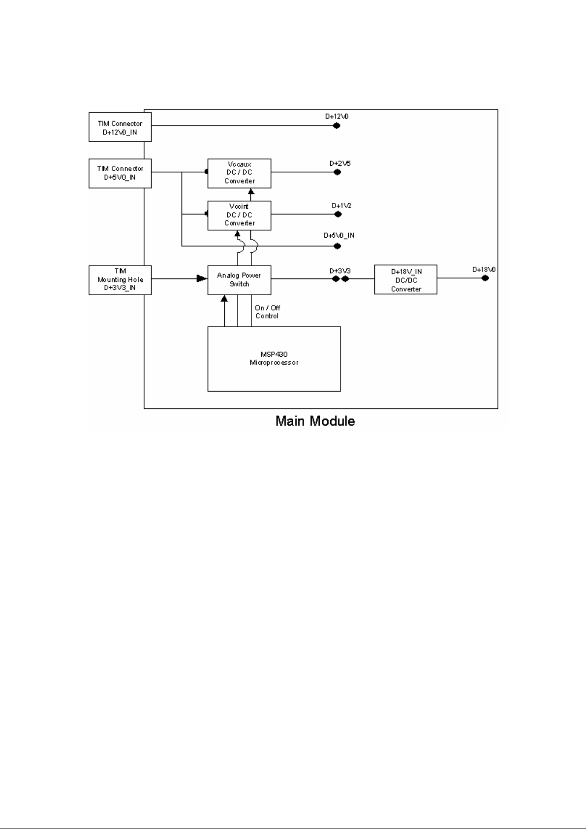
Figure 3. SMT321 Power Structure.
Page 14

TIM
Connector
Reset
POR Reset
Reset Control
FPGA
Fpga
nReset
MSP430
Figure 4. Reset Generation and Distribution.
2.6 MSP Functionality
The MSP430 implements analog control functionality that is difficult to implement in the
FPGA. The microprocessor
• Controls the power start-up sequence
• Controls the reset structure on the module
• Read the temperature from the MAXIM temperature sensor
• Read the serial number from the MAXIM silicon serial number package
The measured information is passed on to the FPGA over a custom bus implementation
between the microprocessor and the FPGA
2.7 Trigger Output
As discussed in the internal data path of the FPGA the triggers operate in two channels
and each channel has three setup registers. Each channel can have a continuous trigger
or a single pulse generated in one channel depending on the multiplexer.
The user configures the triggers via the comports which sets up the trigger registers. The
triggers are made from the system clock (10MHz) which is then scaled by using
counters. Thus if the triggers are set up for a high time of one clock and a low time of
one clock it attains a frequency of 5MHz which is the maximum trigger frequency
Page 15

attainable at the system clock of 10MHz. From here the trigger can be shaped into any
shape as the high and low time are independent of each other.
If the one pulse is activated (and the multiplexer selects the one pulse module) it pulses
the channel with one pulse of a width determined by the pulse high register. If the pulse
high register is set up for one it will pull the channel high for one clock (system clock)
and pull it low indefinitely. In order for another pulse to be generated the pulse module
must receive an enable signal which will once again send a pulse down the channel with
a width depending on the register value.
The two channels are totally independent and thus can be used in this fashion. For
example having a pulse activated on Channel A with a width of 30 clocks and a
continuous trigger on Channel B with a high time of 2 clocks and a low time of 10 clocks.
The trigger outputs are LVPECL. A diagram of the trigger path from the FPGA is shown
in figure 5.
FPGA
TTL to
LVPECL
+ve
-ve
No ground on
connector
Figure 5. Trigger path from FPGA to output.
2.8 Analog Signal Output
As shown in Table 1 the analog signal which is generated in the two analog channels
depends on the VCO present in the channel. The VCO’s are switched by the digital pod
which has two outputs for both VCO’s present on the board. The digital pod can swing
from 0 Volt to 18Volts, but the VCO’s only works from 1 Volt to 16 Volts (High frequency
boards works from 1 Volt – 12 and 15 Volts) which gives a decrease in the pod’s
resolution.
Depending on the VCO model and voltage applied to the VCO an analog signal can be
generated in each channel independent of each other. Figure 6 shows the analog signal
path from the FPGA.
Page 16

FPGA
10dBm (typ)
Control
Digital
Pod
Voltage
Analog signal
VCO
Attenuator
10dBm
Connector
0dBm
output
GND
Figure 6. Analog signal path from FPGA to output.
2.9 Clock Output
The two channels implemented by the clock signals each have its own setup register
which contains a 14bit configuration word. The clocks are generated by the two clock
synthesizers present on the board. And the output is LVPECL.
The user configures the registers via the comports and the resulting clock is then
achieved. When the user writes to the registers the firmware module is automatically
updated and thus the clock.
Each channel can have a different clock running in them as there are two synthesizers
and thus two different clocks. Figure 7 shows the clock path from the FPGA to the
output.
+ve
FPGA
Figure 7. Clock path from FPGA to output.
Clock
Synthesizer
TTL to
LVPECL
-ve
No ground
on connector
2.10 Connectors Pin outs
Figure 8 shows all the connectors on SMT321. Each connector’s pin outs will be
discussed in the following subsections.
Page 17

Figure 8. Connectors present on the SMT321.
2.10.1 FPGA & MSP JTAG connector.
This connector is spilt up into the MSP and FPGA JTAG chain. This cable shown in
figure 9 is used to program both the MSP and FPGA.
Figure 9. Split JTAG Cable for SMT321.
Page 18

2.10.2 Digital IOS
This connector has 14 pins with 8 pins directly connected to a register in the FPGA. The
remaining 6 pins are split up into 3 pins for 3V3 and 3 pins connected to GND. Figure 10
shows the pin assignments on the digital IOS connector.
Figure 10. Digital IOS connector present on the SMT321.
2.10.3 Trigger Connectors
Two trigger output connectors. These triggers are LVPECL thus no ground termination
must be present when implementing or measuring the signal.
2.10.4 Analog Signal Connectors
Two analog signal output connectors. These outputs are analog.
2.10.5 Clock Connectors
Two clock output connectors. These clocks are LVPECL thus no ground termination
must be present when implementing or measuring the signal.
2.11 FPGA IOS
Table 4 shows all of the FPGA’s user IOS. All pins are io standard LVTTL.
Pin Number (IOS
only) Pin Description
1 Trigger output A LVTTL
2 Trigger output B LVTTL
4 Fpga to Dip switch 5 LVTTL
5 Tim Connector 1 LVTTL
6 Tim Connector 2 LVTTL
7 Tim Connector 3 LVTTL
8 Tim Connector 4 LVTTL
10 Tim Connector 5 LVTTL
11 Tim Connector 6 LVTTL
IO
Standard
Page 19

12 Tim Connector 7 LVTTL
13 Tim Connector 8 LVTTL
14 Tim Connector 9 LVTTL
15 Tim Connector 10 LVTTL
17 Tim Connector 11 LVTTL
18 Tim Connector 12 LVTTL
Msp FPGA Bus 0
20
21 Msp FPGA Bus 1 LVTTL
23 Comport0 Control 2 LVTTL
24 Comport0 Control 3 LVTTL
25 Comport0 Control 0 LVTTL
26 Comport0 Control 1 LVTTL
27 Comport0 Data 6 LVTTL
28 Comport0 Data 7 LVTTL
30 Comport0 Data 4 LVTTL
31 Comport0 Data 5 LVTTL
32 Comport0 Data 2 LVTTL
33 Comport0 Data 3 LVTTL
35 Comport0 Data 0 LVTTL
36 Comport0 Data 1 LVTTL
40 Fpga via MSP Config 9 LVTTL
41 Fpga via MSP Config 8 LVTTL
44 Fpga to Dip switch 0 LVTTL
46 Fpga via MSP Config 7 LVTTL
47 Fpga via MSP Config 6 LVTTL
50 Fpga via MSP Config 5 LVTTL
51 Fpga via MSP Config 4 LVTTL
52 Fpga to Dip switch 1 LVTTL
53
55
56
57
58 Fpga via MSP Config 11 LVTTL
59 Fpga via MSP Config 3 LVTTL
60 Fpga via MSP Config 2 LVTTL
63 Fpga via MSP Config 1 LVTTL
65 Fpga via MSP Config 0 LVTTL
68 Fpga to Dip switch 3 LVTTL
69 Fpga to Dip switch 4 LVTTL
70 Fpga to Dip switch 2 LVTTL
73 Comport3 Control 1 LVTTL
(nRESET) LVTTL
EXT10MOsc (Ext
Osscilator) LVTTL
FpgaConfig12 (FPGA
Leds) LVTTL
FpgaConfig13 (FPGA
Leds) LVTTL
FpgaConfig10 (FPGA
Leds) LVTTL
Page 20

74 Comport3 Control 2 LVTTL
76 Comport3 Control 3 LVTTL
77 Comport3 Data 7 LVTTL
78 Comport3 Control 0 LVTTL
79 Comport3 Data 5 LVTTL
80 Comport3 Data 6 LVTTL
82 Comport3 Data 3 LVTTL
83 Comport3 Data 4 LVTTL
84 Comport3 Data 1 LVTTL
85 Comport3 Data 2 LVTTL
86 Msp FPGA Bus4 LVTTL
87 Comport3 Data 0 LVTTL
89 Msp FPGA Bus2 LVTTL
90 Msp FPGA Bus3 LVTTL
92 TimIntControl 2 LVTTL
93 TimIntControl 3 LVTTL
95 TimIntControl 0 LVTTL
96 TimIntControl 1 LVTTL
97 TimClkControl 5 LVTTL
98 Dig IOS Fpga Bus 7 LVTTL
99 TimClkControl 3 LVTTL
100 TimClkControl 4 LVTTL
102 TimClkControl 1 LVTTL
103 TimClkControl 2 LVTTL
104 Dig IOS Fpga Bus 6 LVTTL
105 TimClkControl 0 LVTTL
107 Dig IOS Fpga Bus 4 LVTTL
108 Dig IOS Fpga Bus 5 LVTTL
112 Adjust Clock Control A0 LVTTL
113 Adjust Clock Control A1 LVTTL
116 Dig IOS Fpga Bus 3 LVTTL
118 Adjust Clock Control A2 LVTTL
119 Adjust Clock Control A3 LVTTL
122 Adjust Clock Control B0 LVTTL
123 Adjust Clock Control B1 LVTTL
124 Adjust Clock Control B2 LVTTL
125 Adjust Clock Control B3 LVTTL
127 Adjust VCO Config 5 LVTTL
128 Adjust VCO Config 6 LVTTL
129 Adjust VCO Config 3 LVTTL
130 Adjust VCO Config 4 LVTTL
131 Adjust VCO Config 1 LVTTL
132 Adjust VCO Config 2 LVTTL
135 Dig IOS Fpga Bus 2 LVTTL
Page 21

137 Adjust VCO Config 0 LVTTL
140 Dig IOS Fpga Bus 0 LVTTL
141 Dig IOS Fpga Bus 1 LVTTL
Table 4. User IOS of FPGA in SMT321.
3 Description of interfaces
3.1 MSP430 Interface
A custom interface is implemented between the FPGA and the microprocessor. The
microprocessor is the master and the FPGA is the slave. This interface is used for
issuing a reset command to the FPGA, and for the microprocessor to write the ADC
temperature and silicon serial number to the FPGA.
3.2 Digital Pod Interface
A three wire uni-directional control interface is implemented between the FPGA and the
digital trim-pod. This pod sets the voltage for the VCO’s that generates the analog signal
outputs.
3.3 Clock Synthesizers Interface
A three wire uni-directional control interface is implemented between the FPGA and the
clock synthesizers. These synthesizers control the clock output of the SMT321.
3.4 TIM Interface
The SMT321 implements Comports 0 and 3. All configuration data is received and
transmitted over these two ports. Comport 3 is implemented as a uni-directional receive
interface and only receives data sent to the SMT321. Comport 0 is implemented as a
uni-directional transit interface and only transmits data from the SMT321.
The Global Bus Interface is not implemented on the SMT321. Refer to [1] for a more
detailed description of the TIM interface.
4 Control Register Settings
The Control Registers in the SMT321 control the complete functionality of the SMT321.
These Control Registers are setup via the Comports. The settings of the triggers, the
clock settings and the settings of the analog signals settings can be configured via the
Control Registers.
4.1 Control Packet Structure
The data passed on to the SMT321 over the Comports must conform to a certain packet
structure. Only valid packets will be accepted and only after acceptance of a packet will
Page 22

the appropriate settings be implemented. The first four bits indicate the operation which
must be preformed. There are four operations:
• Comport Reset (bit sequence: 1111)
• Loop back Mode (bit sequence: 0000)
• Comport Register Write Command (bit sequence: 0001)
• Comport Register Read Command (bit sequence: 0010)
The next 12 bits specifies the register to read or write. In the first two commands (Reset
and Loop back) the rest of the packet is NO CARES.
The read command packet only needs the first 2 bytes to read a specific register the last
two bytes are NO CARES.
Write commands use the whole packet, with the last 2 bytes being the data to be written
to the specific register.
This structure is illustrated in the following figure:
Byte Content
Byte Bit 7 Bit 6 Bit 5 Bit 4 Bit 3 Bit 2 Bit 1 Bit 0
0 Command 3 Command
2
1 Address 7 Address 6 Address 5 Address 4 Address 3 Address 2 Address 1 Address 0
2 Data 15 Data 14 Data 13 Data 12 Data 11 Data 10 Data 9 Data 8
3 Data 7 Data 6 Data 5 Data 4 Data 3 Data 2 Data 1 Data 0
Command 1 Command 0 Address
11
Address
10
Address 9 Address
8
Figure 11. Setup Packet Structure.
4.2 Reading and Writing Registers
Control packets are sent to the SMT321 over Comport 3. This is a uni-directional
interface and data can only be sent to the SMT321 over Comport 3. Comport 0 is used
to read control information back from the SMT321. Comport 0 is thus also a unidirectional interface going from the SMT321 to the system host. Data is read by issuing
a ‘Read Request’ control packet containing the address to be read over Comport 3. The
SMT321 will collect the required data and send a ‘Read Packet’ out over Comport 0
containing the requested data. The format of a ‘Read Packet’ is the same as that of a
write packet.
Page 23

1) Write Packet
Command/Address
Byte 0
AddressByte 1
Write DataByte 3
Write DataByte 4
ComPort 3
Host
2) Read Packet
ComPort 0
Command/AddressByte 0
AddressByte 1
Read DataByte 3
Read DataByte 4
SMT321
Figure 12. Control Register Read Sequence.
4.3 Memory Map
The write packets must contain the address where the data must be written to and the
read packets must contain the address where the required data must be read. The
following table shows the memory map for the writable and readable Control Registers
on the SMT321:
Address Writable Registers Readable Registers
0x000 Reserved Firm Ware Version
0x001 Com In Scratch Register 0 Com Out Scratch Register 0
0x002 Com In Scratch Register 1 Com Out Scratch Register 1
0x003 Reserved Smt321 Serial Number A Register
0x004 Reserved Smt321 Serial Number B Register
0x005 Reserved Smt321 Serial Number C Register
0x006 Reserved Smt321 Serial Number D Register
0x007 Reserved Smt321 Air Temp
0x008 Reserved Smt321 Diode Temp
0x009 Reserved Smt321 D1V2 Register
0x00A Clock Control Register A Smt321 D2V5 Register
0x00B Clock Control Register B Smt321 D3V3 Register
0x00C Reserved Smt321 D5V0 Register
0x00D Reserved FPGA Dip Register
. Reserved Reserved
. Reserved Reserved
0x020 Trigger A High Register Reserved
0x021 Trigger A Low Register Reserved
0x022 Trigger B High Register Reserved
0x023 Trigger B Low Register Reserved
0x024 One Pulse A High Register Reserved
0x025 One Pulse B High Register Reserved
Page 24

0x026 Trigger Pulse Multiplexer Channel A Reserved
0x027 Trigger Pulse Multiplexer Channel B Reserved
. Reserved Reserved
. Reserved Reserved
0x030 Digital Pod Register MSB Reserved
0x031 Digital Pod Register LSB Reserved
. Reserved Reserved
. Reserved Reserved
0x040 Digital IOS output register Reserved
Table 5. Register Memory Map.
4.4 Register Descriptions
4.4.1 Com In Scratch Registers
Any value or data can be written to these 16bit registers. These registers are more for
debugging purposes and have no influence in the firmware design.
4.4.2 Clock Control Registers
These registers are used in the setup of the clock outputs of the SMT321. The table
below shows the setup of the registers:
Clock Control Register
Byte Bit 7 Bit 6 Bit 5 Bit 4 Bit 3 Bit 2 Bit 1 Bit 0
0 NO CARES Test Bits Output Division M Count
1 M Count
Table 6. Clock Control setup registers.
As the comport bit stream is 16 bits long both bytes are written simultaneously. The most
significant byte (Byte 0) contains the test bits, output division bits and one M count bit.
The test bits selects between various internal node values and is controlled by the T[2:0]
bits in the serial data stream. The node values are shown in table 7.
Table 7. Test bit configurations.
Page 25

Output division on the clock synthesizers is achieved by the two output division bits
found in the first byte of the clock control registers. There configurations are shown in
table 8.
Table 8. Output division configurations.
The M count bits are used to configure the clock output frequency given all the
constraints set by the hardware and the clock setup bits. The nine bits can be
programmed with any value from 200 – 400 (475 for higher frequency board). All the
setup bits are then used to calculate the output with the following equation.
FXTAL = 16MHz (external oscillator)
N = Value in decimal, set up by the division bits.
M = Value in decimal, set up by the M count bits.
Figure 13. Clock output equation.
For more information refer to the Micrel datasheets [2].
4.4.3 Trigger Control Registers
Registers 0x020 – 0x025 are used for trigger and pulse shaping. Any value from 0 to
65535 (16 bits) can be written into these registers which shapes the triggers and pulses
into high and low times. There are six registers but only 3 influence one channel. The
Trigger A High Register, Trigger B High Register, One Pulse A High Register and One
Pulse B High Register are all high counts (counted in system clocks) of the triggers. Both
the continuous trigger registers (Trigger A High Register and Trigger B High Register)
and the pulse registers (One Pulse A High Register and One Pulse B High Register)
starts counting from one.
Thus if for example the value 2 is written into Trigger A High Register and One Pulse A
High Register the continuous trigger will be high for 2 system clocks and the pulse will
be high for 2 system clocks. The two low registers only have an influence on the
continuous triggers which also needs a low time to shape the trigger. A 1 high 1 low (1 in
high register and 1 in low register) would generate a continuous trigger shown in figure
14.
Figure 14. Trigger with 1 clock high and 1 clock low.
Page 26

The channel can be switch between continuous trigger and pulse with the last two
registers, Trigger Pulse Multiplexers registers 0x026 and 0x027. If a 1 is written into any
of the two that specific channel switches to one pulse generation. If a 0 is written into the
register it switches to continuous trigger for the specific channel. Figure 15 shows how a
one pulse is enabled on the channel.
Figure 15. One pulse generated on trigger A output (ChannelATrigPulse).
If another pulse is needed the pulse high register value must be written again.
4.4.4 Digital Pod Registers
These writable registers are the digital pod control registers. As explained earlier in the
document to configure the digital pod a 24bit data word is needed which is clocked into
the pod. The comports however can only transmit 16 bits of data at a time so two
registers is used and thus an 8 bit waste in the last register. Table 9 shows the two 16 bit
registers contents. The MSB register contains the command, address and data bits. The
LSB register only contains the last 8 bits of data from the word.
Digital Pod Register
Byte Bit 7 Bit 6 Bit 5 Bit 4 Bit 3 Bit 2 Bit 1 Bit 0
0 (MSB) Command Address
1 (MSB) Data
2 (LSB) Data
3 (LSB) NO CARES
Table 9. Digital pod register setup.
These registers are then combined and the last 8 bits left out making a 24 bit word in
firmware which is then clocked into the digital pod.
For more information refer to the Analog Devices digital pod datasheets [3].
4.4.5 Digital IOS output register
This writeable register allows the host to pull the 8 digital IOS present on the SMT321
high or low. Only the first byte (MSB) is used. The packet is shown in table 10.
Digital IOS Register
Byte Bit 7 Bit 6 Bit 5 Bit 4 Bit 3 Bit 2 Bit 1 Bit 0
0 (MSB) Dig IO 7 Dig IO 6 Dig IO 5 Dig IO 4 Dig IO 3 Dig IO 2 Dig IO 1 Dig IO 0
1 (LSB) NO CARES
Table 10. Digital IO register setup.
Page 27

4.4.6 Firm Ware Version
This is a read only register which the host can read the firmware version.
4.4.7 Com Out Scratch Registers
These registers can only be read by the host and in loopback mode the host can write to
the com in scratch registers and read them via the com out scratch registers.
4.4.8 Smt321 Serial Number Registers
The Module Serial Number registers can only be read by the Host. Four registers form a
unique 64 bit silicon serial number.
4.4.9 Smt321 Air Temp and Smt321 Diode Temp
The SMT321 has two temperature measurement registers which can only be read by the
Host. The data is a 255 bit representation of the module temperature measured at the
MSP430. This data must be calibrated to be meaningful.
4.4.10 Voltage registers of the module
These registers are used to store all the voltages present on the module and to be able
to take emergency actions if the voltages are suddenly out of range.
4.4.11 FPGA Dip Register
This register allows the host to read the FPGA dip configuration. There are 6 dips
available thus the status of the dips is the first 6 most significant bits of the received
packet.
Page 28

5 PCB Layout
The following figures shows the top and bottom view of the SMT321.
FPGA +
MSP JTAG
Top Primary TIM Connector
Texas
Inst
MSP430
F149
Power Power
Xilinx Spartan 3
XC3S400
TQ144
Figure 16. Module Top View.
Digital
Pod
Digital IOS
VCO
VCO
Clock
Synhesizer
Clock
Synhesizer
Trig
Chan B
Trig
Chan A
VCO
Chan A
VCO
Chan B
Clock
Chan A
Clock
Chan B
Bottom Primary TIM Connector
Top Primary TIM Connector
Osc
16M
Osc
16M
Figure 17. Module Bottom View.
Inductor Inductor Inductor
Power
Switch
Osc
Bottom Primary TIM Connector
8M
Page 29

6 Waveform Outputs
The following figures show some screen captures of the outputs on the SMT321.
Figure 18. Trigger A: 1 high time 1 low time. Positive side of signal.
Page 30

Figure 19. Trigger B: 10 high time 2 low time. Positive side of signal.
Page 31

Figure 20. Clock B: Freq 62MHz in time. Positive side of signal.
Page 32

Figure 21. Clock B: Freq 62MHz in frequency.
Page 33

Figure 22. Clock B: 233MHz in time. Positive side of signal.
Figure 23. Clock B: 233MHz in frequency.
Page 34

Page 35

Figure 24. VCO2: 247MHz in time.
Page 36

Figure 25. VCO2: 247MHz in frequency.
Page 37

Figure 26. VCO1: 91MHz in time.
Page 38

Figure 27. VCO1: 91MHz in frequency.
Page 39

7 User Manual
The following section describes the use of the SMT321 on a Sundance Carrier using L3
server.
When the application for the SMT321 is generated and run it will start by configuring the
FPGA and then asking the user which SMT321 is present (high frequency or low
frequency). The start up screen will show:
Start FPGA Configuration ...
The FPGA is then configured and when it is done the following messages is shown:
FPGA Configuration Done
.............................................................................................................................................
.............................................................................................................................................
......
After the message is shown the user is prompted to select which SMT321 is present on
the board.
* Specify type of SMT321:
0:Low Freq
1:High Freq
After the user has selected the board configuration a main menu will be displayed.
===================================
| SMT321 Test Software v1.0 |
| Main Menu |
===================================
1: Read SMT321 Firmware Version
2: Write to the SMT321 Scratch Register
3: Read the SMT321 Scratch Register
4: Read SMT321 Temperatures
5: Read the SMT321 Serial Number
6: Read all the SMT321 Voltages
7: Write any command to SMT321
8: Read the SMT321 dip switches
Page 40

9: Setup Trigger A
10: Setup Trigger B
11: Setup VCO 1
12: Setup VCO 2
13: Setup Clock A
14: Setup Clock B
15: Multiplex Trigger A CONT or PULSE
16: Multiplex Trigger B CONT or PULSE
17: Setup Pulse on Trigger A
18: Setup Pulse on Trigger B
23: EXIT
Select:
There are 19 selections available in the menu with the last selection 23 terminating the
program.
The user must select the option by typing in the value of the selection. For example if the
frequency of VCO2 must be set the user will enter 12 and press enter which will then
generate the sub menu for the particular selection (in this case VCO2).
Each selection will now be discussed in the following sections.
7.1 Read SMT321 Firmware Version
This command reads the SMT321 firmware register and displays the contents on the
screen.
7.2 Write to the SMT321 Scratch Register
The user can write to the scratch register by using this command. It has no effect on the
working of the SMT321.
7.3 Read the SMT321 Scratch Register
Reads the scratch register (by default 0x0000).
7.4 Read SMT321 Temperatures
Reads the MAXIM temperature sensor. The sensor will display the local and remote
temperature (local: on the chip self, remote: diode under the fpga).
Page 41

7.5 Read the SMT321 Serial Number
When this command is executed the SMT321 unique serial number is read and
displayed on the screen.
7.6 Read all the SMT321 Voltages
This command reads all the voltage registers (which contains all the voltages present on
the fpga) and displays them.
7.7 Write any command to SMT321
This command enables the user to send any command to the comports. It is mainly used
for debugging and values are sent in 32 bits. The values are entered in decimal. So if the
hex value 0x10200002 is sent to the module the user must enter 270532610d and send
it. This command for example will setup the trigger A high register for 3 high clock
cycles.
A thorough understanding of the SMT321’s registers is needed to use this command
properly.
7.8 Read the SMT321 dip switches
On the SMT321 there resides 8 dip switches which of 6 is connected to the FPGA.
Issuing this command reads the current configuration of the dips and displays it.
7.9 Setup Trigger A
Sets up trigger A by asking the user for the trigger’s high and low time (0 – 65535).
7.10 Setup Trigger B
Sets up trigger A by asking the user for the trigger’s high and low time (0 – 65535).
7.11 Setup VCO 1
The user sets up the VCO1 frequency by giving it a frequency to output (given the
frequency is in the VCO’s range).
Page 42

7.12 Setup VCO 2
The user sets up the VCO2 frequency by giving it a frequency to output (given the
frequency is in the VCO’s range).
7.13 Setup Clock A
The user sets up the required clock frequency (given it is in the correct range) and clock
synthesizers applies this frequency to the clock A output.
7.14 Setup Clock B
The user sets up the required clock frequency (given it is in the correct range) and clock
synthesizers applies this frequency to the clock B output.
7.15 Multiplex Trigger A CONT or PULSE
User selects if trigger line A is a continuous trigger or a single pulse. 0 for continuous or
1 for single pulse.
7.16 Multiplex Trigger B CONT or PULSE
User selects if trigger line B is a continuous trigger or a single pulse. 0 for continuous or
1 for single pulse.
7.17 Setup Pulse on Trigger A
User sets up the pulse on trigger line A (by giving the high time) and generates it. Line
must be set for pulse (option 15).
7.18 Setup Pulse on Trigger B
User sets up the pulse on trigger line B (by giving the high time) and generates it. Line
must be set for pulse (option 16).
 Loading...