

Page 1

SMT310Q
User Manual
User Manual (QCF42); Version 3.1, 31/03/03; © Sundance Multiprocessor Technology Ltd. 2003
Page 2

Version 2.1 Page 2 of 55 SMT310Q User Manual
Revision History
Date Comments
31-10-01 Original Document SP 0.8
20-11-01 Global Bus Accessing AJP 0.9
15-01-02 Final Re-Editing SP 1.0
22-01-02 JTAG performance figures SP 1.1
04-03-02 Comport Mirrors SP 1.2
06-03-02 Comport Int_Control Mirror SP 1.3
29-05-02 Installation Update SP 1.4
13-06-02 AJP 1.5
28-01-03 Editing SP 1.6
24-03-03 General revision PSR 1.7
23-06-03 Firmware upgrade links HV 1.8
07-01-05 EPLDs and EPROM reprogramming SM 1.9
15-07-05 Complement: Section 15. Firmware Updates SM 2.0
20-12-05 Complement: Section 18. LED description MS 2.1
Engineer Version
Page 3

Version 2.1 Page 3 of 55 SMT310Q User Manual
Table of Contents
1. Introduction ....................................................................................................... 6
2. Installing the SMT310Q ..................................................................................... 7
2.1 Software installation ..................................................................................... 7
2.2 Hardware installation.................................................................................... 7
2.3 Testing the hardware.................................................................................... 7
3. Hardware Overview ........................................................................................... 9
3.1 Local Bus ..................................................................................................... 9
3.2 V363EPC PCI Bridge Chip......................................................................... 10
3.3 JTAG controller .......................................................................................... 10
3.4 Shared SRAM ............................................................................................ 10
3.5 Control EPLD ............................................................................................. 10
3.6 Onboard resources..................................................................................... 11
3.6.1 SDB..................................................................................................... 11
3.6.2 Host comport link ................................................................................ 11
4. Comports ......................................................................................................... 12
4.1 C_BUF ....................................................................................................... 12
4.2 Buffered External Comport......................................................................... 16
4.3 Comport to PCI Interface............................................................................ 16
4.3.1 Comport Registers (BAR1, Offset 1016) .............................................. 16
4.3.2 Control Register (BAR1, Offset 1416, WRITE-ONLY).......................... 17
4.3.3 Status Register (BAR1, Offset 1416, Read-Only)................................. 18
4.3.4 Interrupt Control Register (BAR1, Offset 1816) .................................... 19
4.4 Comport Direction ...................................................................................... 19
5. Sundance Digital Bus (SDB)........................................................................... 20
6. JTAG Controller............................................................................................... 21
6.1 Using the SMT310Q External/Internal JTAG with TI Tools. ....................... 22
7. Global/Local Bus Transfers, DSP ↔ PCI. ...................................................... 23
7.1 Mailbox Accesses....................................................................................... 23
7.1.1 Doorbell Interrupts............................................................................... 24
7.2 DSP Interrupt Control ................................................................................. 24
7.3 DSP To Local Aperture 0 control and Accessing ....................................... 25
7.4 DSP Signals ............................................................................................... 26
Page 4

Version 2.1 Page 4 of 55 SMT310Q User Manual
8. Interrupts.......................................................................................................... 29
8.1 SMT310Q-To-PCI Interrupts ...................................................................... 29
8.2 PCI-To-SMT310Q Interrupts ...................................................................... 30
8.3 Interrupt Registers...................................................................................... 30
8.3.1 INTREG Register (BAR1, Offset 4016) ................................................ 31
9. Memory Maps .................................................................................................. 32
9.1 PCI Bus Memory Map ................................................................................ 32
9.1.1 PCI Bridge Chip Internal Register (BAR0) .......................................... 32
9.1.2 I/O Space Register Assignments (BAR1)............................................ 32
9.1.3 Memory Space Assignments (BAR2).................................................. 33
9.1.4 DMA Engine........................................................................................ 33
9.2 Local Bus Memory Map.............................................................................. 34
10. Stand-Alone Mode........................................................................................... 35
11. Specifications .................................................................................................. 36
11.1 Performance Figures.................................................................................. 36
11.2 Relative JTAG speed ................................................................................. 37
11.3 Mechanical Dimensions ............................................................................. 37
11.4 Power consumption.................................................................................... 37
12. Cables and Connectors .................................................................................. 38
12.1 SDB............................................................................................................ 38
12.1.1 SDB Connector ................................................................................... 38
12.2 Comports.................................................................................................... 38
12.2.1 FMS Cabling ....................................................................................... 38
12.2.2 Buffered Comport Cabling................................................................... 39
12.3 JTAG cabling.............................................................................................. 40
12.4 Reset and Config headers.......................................................................... 44
13. Expansion Header (J2).................................................................................... 45
14. JTAG Interface circuits ................................................................................... 46
14.1 Signal Description ...................................................................................... 46
15. Firmware Upgrades ......................................................................................... 48
15.1 CPLD and EPROM reprogramming ........................................................... 49
15.1.1 CPLDs updating .................................................................................. 49
15.1.2 EPROM updating ................................................................................ 51
Page 5

Version 2.1 Page 5 of 55 SMT310Q User Manual
16. Checking for hardware resource conflicts.................................................... 52
17. Where’s that Jumper?..................................................................................... 54
18. LED description............................................................................................... 55
Page 6

Version 2.1 Page 6 of 55 SMT310Q User Manual
1. Introduction
The SMT310Q is a full-length PCI board that can carry up to four, industry-standard,
TIM format processor modules. Sundance provides a large range of these TIMs.
Features:
• Processor interconnection using comports. Direct comport and SDB access to the
host is also provided;
• A software-configurable routing matrix to allow certain comport connectivity
without needing external cables;
• 1MB of shared SRAM between the host and TIM site 1 (the Master TIM site);
• On-board JTAG controller to allow debugging using Code Composer. The board
can also be used as a JTAG master for debugging remote systems;
• On-board PCI bridge chip to provide DMA, mailbox events, and interrupts;
• PCI access between the host and the Master TIM site at burst speeds in the
range 60–100MB/s.
Page 7

Version 2.1 Page 7 of 55 SMT310Q User Manual
2. Installing the SMT310Q
2.1
Software installation
You should install the SMT6300 software package before plugging the
hardware into your PC. The SMT6300 sets up device drivers and test utilities for
the Sundance range of carrier boards.
2.2 Hardware installation
1. Plug your TIMs into the SMT310Q slots. You should normally always
have a TIM in the Master TIM site (nearest the board’s end plate). Note
that many TIMs require a 3.3V supply. This is taken from the mounting
pillars, so it is important you bolt down the modules securely.
2. Power-down the PC;
3. Insert the SMT310Q into a spare PCI slot;
4. Power-up your PC. If you are using1 Windows 2000 or Windows XP, the
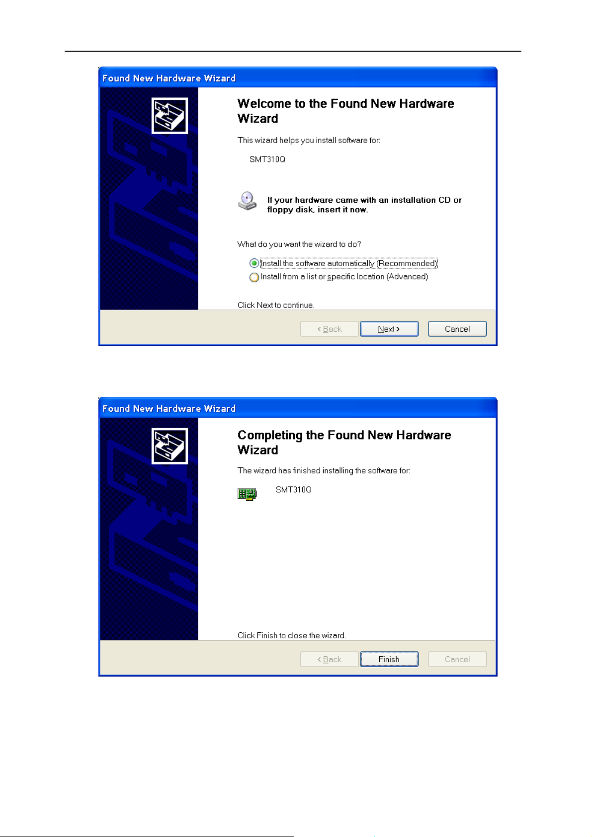
hardware wizard should appear (Figure 1);
5. Click “Next >”. The wizard should indicate that the SMT310Q has been
installed successfully (Figure 2);
6. Click “Finish”.
2.3 Testing the hardware
The SMT6300 comes with a utility called SmtBoardInfo.exe. You should start
this and run its confidence test, found under “Tools”.
1
Windows NT users: No hardware wizard will appear, but you should ensure there are no resource
conflicts. See Checking for hardware resource conflicts
Page 8
Version 2.1 Page 8 of 55 SMT310Q User Manual
Figure 1 - Hardware wizard
Figure 2 - Hardware wizard detected the Sundance hardware
Page 9
Version 2.1 Page 9 of 55 SMT310Q User Manual
3. Hardware Overview
Buffered External
JTAG connector
JTAG In, Internal
JTAG Out, Internal
e
g
d
i
r
B
I
C
P
3
V
32-bit
GLOBAL BUS
SRAM
HOST
comport
Connection
control
HOST
SDB
16-bit
JTAG
TIM 1 TIM 2 TIM 3 TIM 4
8-bit
Buffered
Comport
6 ports
COMPORT CONNECTION MATRIX
8-bit 8-bit 8-bit 8-bit
CBuf FMS FMS FMS
6 ports
7
6 ports
Figure 3 - SMT310Q Block Diagram
6 ports
3.1 Local Bus
The SMT310Q uses a Local Bus
resources. The bus has a 33MHz clock that is available on the CLKIN pin of the
Master TIM site. The TIM in this site should be set to select the local bus clock
in preference to its own oscillator to allow it to synchronise accesses across the
PCI Bridge. Details of this can usually be found in the TIM documentation under
“Global Bus Control Register”.
2
The Local Bus is not shown explicitly in the SMT310Q block diagram.
2
to control transfers amongst the various
Page 10

Version 2.1 Page 10 of 55 SMT310Q User Manual
3.2 V363EPC PCI Bridge Chip
The PCI Bridge connects the host PCI bus to various devices on the local bus:
• Quick Logic EPC363 bridge chip. This has a 32-bit, 33MHz PCI
interface that supports I2C control, mailbox register access, and direct
memory reads and writes;
• Input and output FIFO. This is capable of transferring 256 32-bit words
of data to and from the DSP at 33MHz, bursting at a maximum local bus
transfer rate of 132MB/s;
• Address apertures. These provide access to the V363EPC bridge chip
configuration registers or bridging functions. The apertures respond to
addresses on both the PCI and Local buses. The following apertures are
available on the SMT310Q:
o Four data transfer apertures to transfer data across the bridge.
Two apertures are for PCI to local transfers (BAR1 and BAR2)
and two are for local to PCI transfers (Local-to-PCI Aperture 0 and
Local-to-PCI Aperture 1).
o Two apertures to access the bridge chip’s internal registers: one
aperture for Local Bus (PCI Bridge Register) accesses and one for
PCI bus (BAR0) accesses.
3.3 JTAG controller
The JTAG controller is based on the TI 8990 device; Code Composer Studio
drivers are available from Sundance, Part Number SMT6012. The presence of
a TIM in a module site causes its SENSE pin to switch the module into the
JTAG chain.
3.4 Shared SRAM
The Master TIM can access the SRAM over the Local Bus at transfer rates up
to 100MB/s. The number of wait-states required by the Master TIM varies
depending on the speed of the module. Maximum access rates use a 20ns
strobe cycle.
3.5 Control EPLD
The EPLD acts as an on-board arbitration unit that controls which device has
access to the Local Bus resources.
Page 11

Version 2.1 Page 11 of 55 SMT310Q User Manual
3.6 Onboard resources
3.6.1 SDB
The on-board SDB connector is accessible via the Host PCI interface. It can
be configured with a jumper (J18) to be either an input port or an output port.
It is not intended as a high-speed link as it only has a single 16-bit data
register. You can join this connector with an SDB cable to one of the SDB
connectors on any TIM plugged into the board.
3.6.2 Host comport link
The normal means of communication between the host PC and the Master
TIM on an SMT310Q is through the host comport. A programmable switch
selects how this comport is connected.
Page 12

Version 2.1 Page 12 of 55 SMT310Q User Manual
4. Comports
The SMT310Q gives access to all six comports on each of the four TIM sites3. All of
these comports can be presented at an FMS connector on the rear of the carrier
card. The connectors are marked TxCy, where “x” indicates the TIM site (1–4) and
“y” the comport number (0–5). You can connect pairs of comports by plugging cables
into these FMS connectors. Details of the connections can be found in FMS Cabling.
As an alternative to cables you can use on-board connections that allow for a subset
of the possible topologies. These on-board connections are selected by means of
Quick Switches, programmed from the Host. Figure 4 shows the possible
connections. When the SMT310Q comes out of reset, all the quick switches will be in
the 0 state.
There is a connection from the PCI interface to T1C3. This is enabled by default and
is intended for booting the system. The connection can be changed with the quick
switch controlled by bit D15 in the COM-SWITCH register. The two settings are:
0. Connect the Host Link to T1C3, and connect the C_BUF FMS connector to the
external buffered comport. This allows any of the remaining comports on sites
1—4 to be connected to the external buffered comport with an FMS cable.
In this state, the FMS connector for T1C3 must not be used.
1. Connect the Host Link to the external buffered comport and connect T1C3 to
the C_BUF FMS connector.
4.1 C_BUF
Bit D15 in the COM-SWITCH register determines the connection of the C_BUF
FMS connector (J15):
D15=0 C_BUF FMS is connected to the buffered comport. With jumper J7
fitted, C_BUF FMS will reset as an input. With J7 removed, C_BUF
FMS will reset as an output. See Figure 17.
D15=1 C_BUF FMS is connected to T1C3; this resets to an input.
D15 J7 fitted J7 removed
0 Connect C_BUF to an output comport. Connect C_BUF to an input comport.
1 Connect C_BUF to an output comport.
Not to be used
3
Some TIMs do not implement all six possible comports.
Page 13
Version 2.1 Page 13 of 55 SMT310Q User Manual
A
A
A
r
BC
1
4
1
4
1
4
2
Site 4
5
2
Site 3
5
2
Site 2
5
3
0
3
0
3
0
Host Link
Ex t e r n a l
1
4
Site 1
2
5
3
0
Bu f f e r e d
Comport
- FMS Connecto
- Quic k Switc h
BC
BC
Figure 4: Comport Switching Matrix
Page 14
Version 2.1 Page 14 of 55 SMT310Q User Manual
The Quick Switches are controlled by the COM-SWITCH register (BAR1, offset
2416). The Quick Switch controlled by bit D15 of the COM-SWITCH register has
the following effect:
T1C3
Host Link C BUF
Quick Switch off (0)
Jumper J7 fitted
External
Buffered
Comport
T1C3
T1C3
Host Link C BUF
Quick Switch off (0)
Jumper J7 removed
External
Buffered
Comport
External
Buffered
Comport
Host Link C BUF
Quick Switch on (1)
The switches controlled by all other bits of the COM-SWITCH register have the
following effect:
FMS A FMS B
CP A CP B
Quick Switch off (0) Quick Switch on (1)
CP A CP B
FMS A FMS B
Figure 5: Operation of quick switches
Page 15

Version 2.1 Page 15 of 55 SMT310Q User Manual
D15 D14 D13 D12
PCI-External
T3C3-T4C0 T3C2-T4C5 T3C1-T4C4
T1C3—C_BUF
D11 D10 D9 D8
T2C3-T3C0 T2C2-T3C5 T2C1-T3C4 T1C3-T2C0
D7 D6 D5 D4
T1C2-T2C5 T1C1-T2C4 C-T1C0 B-T1C5
D3 D2 D1 D0
A-T1C4 T4C3-C T4C2-B T4C1-A
Table 1: COM-SWITCH Register
Bit Clear (0) Set (1) Bit Clear (0) Set (1)
D0 T4C1—FMS
D1 T4C2—FMS
T4C1—T1C4
D8
(Requires D3 set)
T4C2—T1C5
D9
(Requires D4 set)
T1C3—FMS
T1C3—T2C0
T2C0—FMS
T2C1—FMS
T2C1—T3C4
T3C4—FMS
D2 T4C3—FMS
D3 T1C4—FMS
D4 T1C5—FMS
D5 T1C0—FMS
T1C1—FMS
D6
T2C4—FMS
T1C2—FMS
D7
T2C5—FMS
T4C3—T1C0
D10
(Requires D5 set)
T1C4—T4C1
D11
(Requires D0 set)
T1C5—T4C2
D12
(Requires D1 set)
T1C0—T4C3
D13
(Requires D2 set)
T2C2—FMS
T2C2—T3C5
T3C5—FMS
T2C3—FMS
T2C3—T3C0
T3C0—FMS
T3C1—FMS
T3C1—T4C4
T4C4—FMS
T3C2—FMS
T3C2—T4C5
T4C5—FMS
T1C1—T2C4 D14 T3C3—FMS T3C3—T4C0
T1C2—T2C5 D15
C_BUF—External
Buffered Comport
PCI—T1C3
PCI— External
Buffered Comport
T1C3—C_BUF
Page 16

Version 2.1 Page 16 of 55 SMT310Q User Manual
4.2 Buffered External Comport
The buffer consists of an FCT245AT type device with 64mA pull-down ability. All
signals are pulled up to +3.3 volts with 100-ohm resistors and the active devices
are mounted as closely as possible to the connector they serve. The back panel
connector is a 26 pin 3M type (3M part number 10226-5212JL).
As well as ground signals and the 12 C4x comport signals, there are 6 additional
signals. These signals are NOT essential for communications:
Name Description
I/O_OUT Output high when port is outputting, output low when port is receiving.
I/O_IN Input which prevents bus contention if connected to I/O_OUT
/RST_OUT Active low open collector copy of the board reset drive.
/RST_IN Active low board reset input, pulled up to 3.3V by 100 ohms.
VCC 1 AMP +5 Volt supply, with resetable 1 Amp fuse, to power a remote buffer, if
required.
SHIELD Overall cable shield, connected to plug shells and chassis.
Table 2: Buffered Comport Additional Signals
You can synchronise resetting a number of boards by chaining them together
with /RST_OUT of one driving /RST_IN of the next.
The SMT502-Buffer is the recommended cable assembly for the buffered
comport and can be purchased separately.
4.3 Comport to PCI Interface
The comport interface is memory-mapped to the PCI bridge as illustrated in
Table 8. The comport uses the control and data registers to detect the state of
the input and output FIFOs. The following section describes the bit definitions
for these registers.
4.3.1 Comport Registers (BAR1, Offset 1016)
The host can be connected to TIM site 1 using comport 3 (T1C3). This port is
bi-directional and will automatically switch direction to meet a request from
either the host or the DSP. Both input and output registers are 32 bits wide.
Data can only be written to COMPORT_OUT when STATUS [OBF] is 0. When
a word is received from the DSP, it is stored in COMPORT_IN and STATUS
[IBF] is set to 1. Reading COMPORT_IN will clear STATUS [IBF] and allow
another word to be received from the DSP.
Page 17
Version 2.1 Page 17 of 55 SMT310Q User Manual
4.3.2 Control Register (BAR1, Offset 1416, WRITE-ONLY)
The CONTROL register contains various control flags:
7-4 3 2 1 0
IIOF2 IIFO1 IIOF0 RESET
RESET Write a 1 to this bit to assert the reset signal to all the TIM modules on
the SMT310Q.
IIOF0
IIOF1
IIOF2
These bits connect to the corresponding pins on the TIM in module site
1. Writing 0 causes the corresponding IIOF line to go low.
Table 3: Control Register
Note. On PCI system reset, RESET is asserted to all TIM sites.
Page 18

Version 2.1 Page 18 of 55 SMT310Q User Manual
4.3.3 Status Register (BAR1, Offset 1416, Read-Only)
31-22 21 20 19 18 17 16 15-12 11 10 9 8
CONFIG_L TBC RDY 0 MASTER IBF OBF IM2 IM1 IM0 INTD
7 6 5 4 3 2 1 0
C40 INT TBC INT IBF INT OBE INT C40 IE TBC IE IBF IE OBE IE
OBE IE Set if comport output buffer empty interrupts enabled.
IBF IE Set if comport input buffer full interrupts enabled
TBC IE Set if JTAG interrupts enabled
C40 IE Set if interrupt from TIM DSP enabled
OBE INT Set if the comport output buffer becomes empty. Cleared by writing a 1 to the
corresponding bit in the interrupt control register.
IBF INT Set if the comport input buffer receives a word. Cleared by writing a 1to the
corresponding bit in the interrupt control register
TBC INT Set when the TBC asserts its interrupt. Cleared by removing the source of the
interrupt in the TBC.
C40 INT Set when the TIM DSP sets its host interrupt bit. Cleared by writing a 1 to the
corresponding bit in the interrupt control register.
INTD The logical OR of bits 7—4 in this register gated with each one’s enable bit.
OBF Set when a word has been written to the comport output register. Cleared when the
word has been transmitted to the DSP.
IM0 Interrupt mask 0. Returns Interrupt Control Register Bit 8.
IM1 Interrupt mask 1. Returns Interrupt Control Register Bit 9.
IM2 Interrupt mask 2. Returns Interrupt Control Register Bit 10.
IBF Set when a word has been received into the comport input register.
MASTER Set when the SMT310Q bridge owns the comport interface token.
TBC RDY Reflects the current state of the TBC RDY pin. This bit is active high and therefore
is an inversion of the TBC pin.
CONFIG_L Reflects the state of the TIMs’ CONFIG signal. Active low.
Table 4: Status Register
INTD is the input interrupt into the PCI Bridge from the SMT310Q; this can be
routed to INTA, INTB, or INTC using the PCI Interrupt Configuration Register
(BAR0, offset 4C
16
).
Page 19

Version 2.1 Page 19 of 55 SMT310Q User Manual
4.3.4 Interrupt Control Register (BAR1, Offset 1816)
This write-only register controls the generation of interrupts on the PCI bus.
Each interrupt source has an associated enable and clear flag. This register can
be written with the contents of bits 7:0 of the Status Register. The JTAG
controller generates TBC INT and must be cleared of all interrupt sources in
order to clear the interrupt.
10 9
DSP-PC IIOF2 En DSP-PC IIOF1 En
8 7 6 5 4 3 2 1 0
DSP-PC
IIOF0 En
CLEAR
C40 INT
0 CLEAR
IBF INT
CLEAR OBE
INT
C40 IE TBC IE IBF IE OBE IE
DSP-PC IIOF2 En Enables DSP-PC interrupts on IIOF2
DSP-PC IIOF1 En Enables DSP-PC interrupts on IIOF1
DSP-PC IIOF0 En Enables DSP-PC interrupts on IIOF0
IBF IE Comport Input Buffer Full Interrupt Enable. Allows an interrupt to be generated
when the host comport input register is loaded with data from the C40.
OBE IE Comport Output Buffer Empty Interrupt. Allows an interrupt to be generated
when the host comport register has transmitted its contents.
TBC IE Test Bus Controller Interrupt Enable. Interrupts from the Texas JTAG controller
are enabled when set.
C40 IE C40 Interrupt Enable. Allows a programmed interrupt to be generated by the
C40 when set.
CLEAR OBE INT Write a one to this bit to clear the interrupt resulting from a comport output
event.
CLEAR IBF INT Write a one to this bit to clear the interrupt event resulting from comport input.
CLEAR C40 INT Write a one to this bit to clear down the C40 INT event.
Table 5: Interrupt Control Register
4.4 Comport Direction
Comports will automatically switch direction during the execution of a program,
but when they come out of reset, they will be set to an initial direction: input or
output. You should always ensure that you only ever connect pairs of comports
that reset to opposite initial directions.
Comports resetting as inputs 3, 4, 5
Comports resetting as outputs 0, 1, 2
Page 20

Version 2.1 Page 20 of 55 SMT310Q User Manual
5. Sundance Digital Bus (SDB)
A growing number of Sundance’s Modules have an on-board SDB. A description of
the SDB interface may be found on the Sundance web site at
www.sundance.com/html/pdf_info.htm.
The following register controls the carrier’s SDB.
D7 D6 D5 D4 D3 D2 D1 D0
X X OFFF IPFF RW RW RW RXNTX
Table 6: SDB Control Register
The SDB control and status register is located at BAR2 offset 0020026016. The bit
definitions are shown below:
RXNTX
RW
IPFF
OPFF
SDB Direction. The SDB direction is set using Jumper J18 (
SMT310Q, When the jumper is removed the SDB is set for receive mode; when the
jumper is present the SDB is set for transmit mode. This bit indicates the direction
set: 0=Receive, 1=Transmit.
General scratch bits
Input FIFO full: When set, a 16-bit value has been latched in the data register ready
for reading. This bit is automatically cleared on a read from the data register.
Output FIFO full: This bit is set when a 16-bit value is written to the FIFO and is
automatically cleared when it has been sent out of the SDB.
Figure 17) on the
The SDB data register is located at BAR2 offset 0020024016. You can write 16-bit
values to this location to transfer them over the SDB interface as long as the OPFF
flag in the status register is clear and the J18 jumper is present.
Page 21

Version 2.1 Page 21 of 55 SMT310Q User Manual
6. JTAG Controller
The SMT310Q has an on board Test Bus Controller (TBC), an SN74ACT8990 from
Texas Instruments. The TBC is controlled from the PCI bus giving access to the onsite TIMs and any number of external TIMs. Please refer to the Texas Instruments
data sheet for details of this controller. The TBC is accessed in I/O space BAR1
offset 8016.
Te s t B us
Switc hing
Matrix
Test Bus
Con troller
XDS-510
compatible
JTAG ou t
Site 1 Site 2 Site 3 Site 4
Buffered
JTAG
Connecto r
Buffers
XD S- 51 0
compatible
JTAG i n
PCI bridge
Figure 6: TBC Data Routing
The SMT310Q can operate in two TBC modes; Master mode and Slave mode. In
Master mode, the Test Bus Controller on the SMT310Q drives the JTAG scan chain
through the TIM sites on the SMT310Q. If any or all the sites are not populated with a
TIM then the module’s SENSE signal is used to enable a tri-state buffer connecting
TDI and TDO (JTAG Data In and Data Out) on the specific site, maintaining the
integrity of the JTAG data path. This switching is automatic. The Buffered External
JTAG Connector J5 is intended to connect to a JTAG device external to the system
chassis. When the SMT310Q is in master mode, the buffered JTAG connector acts
as a master and is to be connected to JTAG slaves. The un-buffered JTAG out (XDS-
510) Header J11 is for use with JTAG slaves within the system chassis. When either
of these connectors is connected to a JTAG slave device, the SMT310Q
automatically detects the device and routes the test data accordingly. Master mode is
selected with a jumper in location A on J3.
When the SMT310Q is configured in Slave mode, the TBC on the SMT310Q is
disabled, as the TBC is assumed to be on another device connected to the
SMT310Q. If using a TBC device within the same system chassis, the connection
can be made using the XDS-510 compatible connector J14.
Page 22

Version 2.1 Page 22 of 55 SMT310Q User Manual
In this case, the XDS-510 compatible connector must be selected as the JTAG
source by fitting a jumper on J3 in location B. If the TBC device is out side the system
chassis, then the External Buffered JTAG connector J5 should be used. Again, this
connector must be selected as the JTAG source by fitting a jumper on J3 in location
C. The jumpers J3, J5, J11, and J14 can be found in Figure 17.
Important Note:
There must only ever be one jumper fitted in J3
Multiple SMT310Qs can be cascaded in a JTAG chain, but the master device must
drive out through either the buffered JTAG or the XDS-510 header, not both.
If you require all modules to be reset when using multiple SMT310Qs, the Reset In
and Reset Out headers must be chained together. See Reset and Config headers.
There are three cable options for the SMT310Q:
• SMT501-JTAG is designed to connect two SMTxxx carrier boards, for
example, an SMT310Q controlling an SMT328 VME carrier. The length of
SMT501-JTAG is 1 meter.
• SMT510-XDS is a variant of the SMT501-JTAG, providing an XDS-510 14-
way connector to interface to non-Sundance products.
• SMT503-JTAG-INT is used to connect to the un-buffered XDS-510 compatible
JTAG in and out headers
6.1 Using the SMT310Q External/Internal JTAG with TI Tools.
For details on using the SMT310Q with Texas Instruments Code Composer, see
the SMT6012 documentation.
The SMT6012 is Sundance’s driver for Code Composer and can be obtained
separately.
The Texas Instruments Evaluation Module (EVM) kits can be used as stand-alone
devices with an SMT310Q as the JTAG master. When running with the EVM kits
ensure that the EVM jumper is set up correctly: External JTAG must be selected
and the DSP boot location must be set for internal memory space.
Page 23

Version 2.1 Page 23 of 55 SMT310Q User Manual
7. Global/Local Bus Transfers, DSP ↔ PCI.
The traditional global bus interface on C6x DSP modules interfaces to the SMT310Q
via a local bus. This allows Global bus transfers on the DSP to be converted into
local bus accesses, giving direct DSP accesses to the PCI bridge chip.
The resources in the PCI bridge chip are illustrated in the figure below.
PCI Bridge Device
MailBox
Read/Write
Interrupt Control
Local To PCI Bus
Apperture Control
LOCAL <-> PCI
Apperture 0
16MB Address
Space
Local Bus
Arbitration
Unit
DSP Global
Bus Access
Figure 7: Local Bus to DSP Connectivity
7.1 Mailbox Accesses
The mailbox registers can be used to transfer commands or small amounts of
data between the PCI bus and the DSP, via the local bus. The PCI bridge
device provides 16 8-bit mailbox registers, which may be used to communicate
data between the DSP and Host.
The mailbox registers are accessed from the DSP through the Local-to-Internal
Register (LB_IO_BASE) aperture. As illustrated in section 5, table 4 of this
document, this region is accessed by the DSP via a global bus access to the
PCI Bridge Registers (Address: 1C00000016).
Page 24

Version 2.1 Page 24 of 55 SMT310Q User Manual
The mailbox registers are on byte boundaries with offsets C016–CF16, from
LB_IO_BASE. As all DSP global bus accesses are carried out in aligned 4-byte
units, a write access over the global bus to 1C00000016 + C016 will write to the
first 4 mailbox registers in the PCI bridge device.
The mailbox registers are accessed from the PCI bus through the PCI-toInternal Register (PCI_IO_BASE) aperture. This is accessed via the PCI Bridge
Chip Internal Register (BAR0, byte offset C016–CF16).
7.1.1 Doorbell Interrupts
Each of the 16 mailbox registers can generate four different interrupt requests
called doorbell interrupts. Each of these requests can be independently
masked for each mailbox register. The four doorbell interrupt types are:
• DSP interrupt request on read from PCI side
• DSP interrupt request on write from PCI side
• PCI interrupt request on read from DSP side
• PCI interrupt request on write from DSP side
The PCI read and DSP read interrupts are ORed together and latched in the
mailbox read interrupt status register (MAIL_RD_STAT). Similarly, the PCI
write and DSP write interrupts are ORed together and latched in the mailbox
write interrupt status register (MAIL_WR_STAT). All of the interrupt request
outputs from the status registers are ORed together to form a single mailbox
unit interrupt request and routed to both the Local and PCI Interrupt Control
Units.
When several mailbox registers are accessed simultaneously, for example
when 4 mailbox registers are read as a word quantity, then each register
affected will request a separate interrupt if programmed to do so.
See section
8. for further information on Interrupts.
7.2 DSP Interrupt Control
Interrupts can be enabled from a number of different sources i.e. DSP►Host
and Host►DSP. See section 8. for a description of these functions.
Page 25

Version 2.1 Page 25 of 55 SMT310Q User Manual
7.3 DSP To Local Aperture 0 control and Accessing
The quickest way to transfer information between the DSP and PCI Bus is to
use the Local-to-PCI Aperture 0 in the PCI bridge device.
A DSP may need to transfer large amounts of acquired data to the PC host for
data storage or post-processing. Allowing the DSP to take control of the PCI
bus means that the HOST only needs to be involved once the data have been
transferred by the DSP to PC memory. Alerting the Host that data have been
transferred can be accomplished in a number of ways, for example, by writing to
a mailbox register to generate an interrupt.
The Local-to-PCI Aperture 0 is mapped as a region of addressable space from
1800000016–183FFFFF16 (words), as shown in Table 4, section 5.
There are several registers to initialise before data can be read or written via
this address space:
• Unlock the PCI Bridge System register. This requires a write to the
LB_CFG_SYSTEM (offset 7816, BAR 0) with the value A05F
16
.
• Write the upper 8 bits of your destination address (in bytes) to the upper
8 bits of the 32-bit Local Bus to PCI Map 0 register (LB_MAP0_RES,
offset in bytes 5c16).
• Convert you lower 24-bit address to a word aligned value.
• Write/Read data using Local-to-PCI Aperture 0.
Page 26

Version 2.1 Page 26 of 55 SMT310Q User Manual
7.4 DSP Signals
AE*/DE* active low address/data enable signals driven by the SMT310Q.
When the DSP has ownership of the bus, these signals are driven
low by the SMT310Q allowing the DSP to drive the address and
data pins.
CE0*
STRB1*
RDY1*
STAT0
STAT1
STAT2
STAT3
A0–A30
D0–D31
the tri-state control for the DSP’s global bus control pins. This is
permanently tied low by the SMT310Q, as the control signals are
always enabled.
the data strobe signal from the DSP’s global bus. It is driven low
when the DSP is carrying out an access cycle. The DSP waits for
RDY1* to be driven low by the SMT310Q to indicate transfer has
been completed. This transfer is carried out in synchronous burst
mode. The DSP pulls STAT0 low to signal when the burst transfer
has completed.
an active low transfer acknowledgement, driven by the SMT310Q to
indicate that the current transfer has been completed.
the DSP Status line. When all of the signals are logic ‘1’ then the
DSP Global bus interface is in an idle state. When any of these
signals is driven low, the DSP is requesting ownership of the
SMT310Q’s local bus. STAT0 has a special meaning and is driven
low by the DSP to indicate the last data packet transfer.
the DSP’s global Bus address lines.
the DSP’s global Bus data lines
IIOF0
IIOF1
IIOF2
DSP Interrupt signals. These are open-collector signals on the
SMT310Q that can be driven by the DSP interrupt the host, or
driven by the host to interrupt the DSP
Page 27

Version 2.1 Page 27 of 55 SMT310Q User Manual
In the timing diagram below all signals change relative to the rising LCLK signal.
This signal is the H1 clock signal of the DSP when using the DSP global bus in
synchronous mode.
LCLK
STAT
STRB1
RDY1
STAT0
AE/DE
A[30..0]
D[31..0]
TIMReq FIFO Full
Figure 8: Timing diagram for DSP local bus access
LCLK Period =30ns, frequency is 33MHz.
The DSP initiates a global bus R/W by asserting the STRB1 low and STAT[1:3]
change (see the TIM Spec for details of STAT[1..3]). Once the arbitration unit
detects this, it waits for the last cycle of the Local bus to be completed by the
PCI bridge, before allowing the DSP to become Bus Master. Once the DSP is
Master the arbitration unit drives AE and DE low to enable the DSP’s address
and data lines. RDY1 is driven low by the arbiter to indicate to the DSP, on the
next rising LCLK, that the data packet has been transferred. If the input FIFO
(256 words deep) becomes full, the arbitration logic de-asserts the RDY1 signal
to indicate a hold-off state.
Once the data have been transferred from the FIFO to the PCI bus, RDY1 is reasserted to continue the transfer. Asserting STAT0 low indicates the end of the
burst access. If RDY1 is not active then STAT0 should remain asserted until
ready is asserted and the final data transaction has been completed.
It is possible for a deadlock condition to arise if the PCI bus is trying to read
from the SMT310Q resources while the DSP is reading from the PCI Bus. If
this happens, the arbitration unit gives the PCI bridge device priority and
services the HOST PCI access before giving bus ownership back to the DSP.
Page 28

Version 2.1 Page 28 of 55 SMT310Q User Manual
When running code composer applications to debug the DSP a reduction in the
speed of the debugger may be noticed. The DSP has priority when accessing
the local bus and any other accesses will only occur under the following
conditions.
• Burst access finishes
• A deadlock condition occurs which forces the DSP to release ownership
of the Bus.
For multi-threaded applications the length of the DSP burst can be reduced to
allow PCI bus R/W cycles snatch cycles from the DSP.
Page 29

Version 2.1 Page 29 of 55 SMT310Q User Manual
8. Interrupts
8.1 SMT310Q-To-PCI Interrupts
CONTROL EPLD
INTERRUPT
CONTROL
REGISTER
C40 IE
IBF IE
OBE IE
TBC IE
INTD
INTD
TIMIIOF0
TIMIIOF1
TIMIIOF2
JTAG INT
INTERRUPT
CONTROL
REGISTER
DSP IIOF0
ENABL E
DSP IIOF1
ENABL E
DSP IIOF2
ENABL E
STATUS
REGISTER
DSP INT
IBF INT
OBE I NT
TBC INT
Figure 9: SMT310Q to PCI Interrupts
Interrupts can also be generated by the SMT310Q writing or reading the
mailbox registers in the PCI Bridge.
PCI Bridge
INTA
INTB
INTC
Page 30

Version 2.1 Page 30 of 55 SMT310Q User Manual
8.2 PCI-To-SMT310Q Interrupts
CONTROL CPLD
CONTROL
REGISTER
PCI
Bridge
LINT can
be caused
by any PCI
interrupt
e.g. Mailbox
LINT
LINT
IIOF0
IIOF1
IIOF2
INTRE G
REGISTER
TIMIIOF0 IE
TIMIIOF1 IE
TIMIIOF2 IE
TIMIIOF0
TIMIIOF1
TIMI IOF 2
Figure 10: PCI to SMT310Q Interrupts
8.3 Interrupt Registers
The following registers are used to control PCI►DSP and DSP►PCI interrupts:
• PCI bridge internal register
• PCI Interrupt Configuration (BAR 0, 4C16)
• PCI Interrupt Status (BAR 0, 4816)
• Local Bus Interrupt Mask (BAR 0, 7716)
• Local Bus Interrupt Status (BAR 0, 76
• PCI Mailbox Write Interrupt Control (BAR 0, D0
16
)
16
• PCI Mailbox Read Interrupt Control (BAR 0, D216)
• Local Bus Mailbox Write Interrupt Control (BAR 0, D416)
• Local Bus Mailbox Read Interrupt Control (BAR 0, D616)
• Mailbox Write Interrupt Status (BAR 0, D816)
• Mailbox Read Interrupt Status (BAR 0, DA16)
)
Page 31

Version 2.1 Page 31 of 55 SMT310Q User Manual
Details of these registers can be found in the V363EPC Local Bus PCI Bridge
User Manual:
(http://www.quicklogic.com/home.asp?PageID=223&sMenuID=114#Docs)
Other Registers
Control Register (BAR1, Offset 1416, WRITE-ONLY)
Interrupt Control Register (BAR1, Offset 1816)
INTREG Register (BAR1, Offset 4016)
8.3.1 INTREG Register (BAR1, Offset 4016)
Bits Name Description
15 - Reserved
14 - Reserved
13 - Reserved
12 - Reserved
11 - Reserved
10 - Reserved
9 - Reserved
8 - Reserved
7 - Reserved
6 - Reserved
5 - Reserved
4 - Reserved
3 -
2 IIOF2EN PC to DSP TIMIIOF2 interrupt enable
1 IIOF1EN PC to DSP TIMIIOF1 interrupt enable
0 IIOF0EN PC to DSP TIMIIOF0 interrupt enable
Reserved
Table 7: INTREG Register
Page 32

Version 2.1 Page 32 of 55 SMT310Q User Manual
9. Memory Maps
All address information is given in bytes:
9.1 PCI Bus Memory Map
9.1.1 PCI Bridge Chip Internal Register (BAR0)
Please see the User Manual for the V363EPC Local Bus PCI Bridge chip,
http://www.quicklogic.com/home.asp?PageID=223&sMenuID=114#Docs, for
details of internal registers.
9.1.2 I/O Space Register Assignments (BAR1)
In target mode, a host device accesses the SMT310Q across the PCI bus,
which gives access to the target mode registers. The operating system or
BIOS will normally allocate a base address for the target mode registers of
each SMT310Q. Access to each register within the SMT310Q is then made at
offsets from this base address as shown in the table below.
Offset Register (Write) Register (Read) Width
00
16
04
16
08
16
0C
16
10
16
14
16
18
16
1C
16
20
to 3F
16
24
16
40
16
8016 to AF
- -
- -
- -
- -
COMPORT_OUT COMPORT_IN 32
CONTROL STATUS 32
INT_CONTROL 32
- -
COMPORT Configuration COMPORT
16
COM_SWITCH COM_SWITCH 16
INTREG
TBC Write TBC Read 16
16
Configuration
INTREG
16
Table 8: I/O address space map
Page 33

Version 2.1 Page 33 of 55 SMT310Q User Manual
9.1.3 Memory Space Assignments (BAR2)
Address Description Notes
0000000016–000FFFFF
00200090
00200094
00200098
0020000016–0020007F
0020024016–0020 025F
0020026016–0020027F
Note 1: In order for the TIM to respond to accesses for this area address line
GADD30 and GADD19 of the TIM site connector must be decoded as high
and GADD7 and GADD5 must be decoded as low.
16
16
16
16
16
16
16
Shared Memory Bank
Comport Data Mirror
Comport Status Mirror
Comport Int_Control Mirror
Global Bus
SDB Data Register
SDB Control Register
Table 9: Memory space map
1MB SRAM
Mirror of COMPORT_OUT /
COMPORT_IN
See Note 2
Mirror of Control / Status
See Note 2
Mirror of Int_Control
See Note 2
See Note 1
Input/Output 16 bit SDB
Interface
SDB Control/Status
Note 2: These mirrors of addresses in the I/O Space (BAR1) allow increased
transfer speeds across the host comport link (in excess of ×10 increase).
9.1.4 DMA Engine
The PCI Bridge DMA processor sees the shared memory at a different
address from that used for normal accesses. For normal memory access the
memory base address register offset is 0000000016. For DMA access address
line A28 (On hardware interface) must be high, therefore DMA memory access
starts at 4000000016 (not 1000000016 as addressing is in bytes).
Page 34

Version 2.1 Page 34 of 55 SMT310Q User Manual
9.2 Local Bus Memory Map
The table below illustrates the resources and their corresponding address
regions when accessed by the Master module.
Local bus access Description Notes
1800000016–183FFFFF
1400000016–17FFFFFF
1C00000016–1C0000FF
D000000016–D00FFFFF
Local-to-PCI Aperture 0 PCI Bridge Aperture 0 Space
16
Local-to-PCI Aperture 1 PCI Bridge Aperture 1 Space
16
16
16
PCI Bridge Registers PCI Bridge Internal resisters
Shared Memory Bank 1MB SRAM
Table 10: Memory space map
Page 35

Version 2.1 Page 35 of 55 SMT310Q User Manual
)
)
)
)
)
)
)
)
10. Stand-Alone Mode
For the SMT310Q to operate in stand-alone mode Jumper J8 (Figure 17: Jumper
Finder Diagram) must be installed and the Auxiliary power header (J1) connected.
The plug for power connector is AMP part No 640440-8. The connector requires
wiring as shown in the pin diagram below. Wire of 0.3 mm2 core (22 AWG) should be
used.
1
2
3
4
5
6
7
8
+12V
1
-12V
2
+5V
3
+5V
4
+3.3V
5
+3.3V
6
GND
7
GND
8
Figure 11: Auxiliary Power Connector
Page 36

Version 2.1 Page 36 of 55 SMT310Q User Manual
11. Specifications
11.1
Performance Figures
The following performance figures are for the SMT310Q with the Rev. A1 V3
PCI bridging device fitted and using a SMT335. Further performance figures
will be issued as faster V3 PCI bridging devices become available and are fitted
to the SMT310Q.
The figures shown below may vary greatly depending on the application. Some
of the issues are:
• PC Architecture and performance
• Transfer parameters.
• The transfer size.
• Frequency of transfer.
• The layout of the target memory. (Scatter/Gather or contiguous)
• Availability of the PCI bus.
• Other devices on the PCI bus.
• Debugging traffic on the bus.
• Comport traffic.
Transfer
type
C60 Burst
Read To Host
Memory
C60 Burst
Write To Host
Memory
MIN
(Mb/s)
Table 11: Performance Figures
MAX
(Mb/s)
45 82 70
11 88 68
AVERAGE
(Mb/s)
Comments
Will Vary depending
on PCI traffic
Will Vary depending
on PCI traffic
Page 37

Version 2.1 Page 37 of 55 SMT310Q User Manual
11.2 Relative JTAG speed
Relative Emulator Speeds
3.00
2.50
2.00
1.50
1.00
1.00
0.50
Speed relative to XDS510
0.00
XDS510 FleXDS SPI525 XDS510PP
1.67
Figure 12: JTAG speed Comparison chart
11.3 Mechanical Dimensions
The board size is 312mm × 120mm
1.25
0.85
Plus
2.70
1.62
1.20
0.60
SPI515 XDS510PP Tiger SMT106 SMT310Q
Emulator
0.50
11.4 Power consumption
The SMT310Q takes 3.3V and 5V power from the PC’s internal power supply.
The following current consumption figures were measured using a LEM current
clamp during a quiescent period.
Current drawn from 3.3v supply: 440mA
Current drawn from 5v supply: 100mA
Page 38

Version 2.1 Page 38 of 55 SMT310Q User Manual
12. Cables and Connectors
12.1
SDB
No SDB cables are supplied with the SMT310Q. You can order them separately
from Sundance with part number SMT510-SDBxx, where xx is the cable length
in centimetres.
12.1.1 SDB Connector
Function Pin Pin Function Function Pin Pin Function
GND 2 1 CLK D9 21 22 GND
GND 4 3 D0 D10 23 24 GND
GND 6 5 D1 D11 25 26 GND
GND 8 7 D2 D12 27 28 GND
GND 10 9 D3 D13 29 30 GND
GND 12 11 D4 D14 31 32 GND
GND 14 13 D5 D15 33 34 GND
GND 16 15 D 6 USERDEF0 35 36 GND
GND 18 17 D7 WEN 37 38 REQ
GND 20 19 D8 USERDEF1 39 40 ACK
Table 12: SDB Pin-out
12.2 Comports
12.2.1 FMS Cabling
The cables used with FMS connectors are not supplied with the SMT310Q.
You can order them separately from Sundance with part number SMT500FMSxx, where xx is the cable length in centimetres.
When fitting FMS cables, make sure they have a twist: one end must have the
blue side facing out and the other must have the silver side facing out.
Important Note.
If using FMS cables between two SMT310Qs4 the reset headers must be
connected to ensure that all comports reset at the same time.
See Reset and Config headers
4
This is not recommended as long FMS cables can introduce communication problems.
Page 39

Version 2.1 Page 39 of 55 SMT310Q User Manual
Pin No. Signal Pin No. Signal
1 GND 2 DATA0
3 DATA1 4 DATA2
5 DATA3 6 DATA4
7 DATA5 8 DATA6
9 DATA7 10 /CREQ
11 /CACK 12 /CSTRB
13 /CRDY 14 GND
Figure 13: FMS connector pin out
12.2.2 Buffered Comport Cabling
Connecting between buffered comports requires a 1 to 1 cable; the SMT502Buffer is the recommended cable assembly and can be purchased separately.
Cable plugs 3M Scotchflex 10126-6000EL FES part 038740A
Plug shells 3M Scotchflex 10326-A200-00 FES part 038760D
Cable type 3M Scotchflex KUCKMPVVSB28-13PAIR FES
part 038781E
This cable has 13 individual pairs, with an overall shield, and an outer
diameter of 7mm. Cable length should be as short as possible. The maximum
tested cable length is 1 meter.
On reset, each comport initialises to being either an input or an output.
Do not connect ‘Reset to Input’ comports together.
Do not connect ‘Reset to Output’ comports together.
However if this should occur, no damage will result, because comport direction
signals disable relevant comports.
Page 40

Version 2.1 Page 40 of 55 SMT310Q User Manual
The following table shows connector pin-out and cable pair connections. This
is important, as the critical signals must be paired with a ground as shown.
The allocation to twisted pairs is based on grouping the data signals because
they change at the same time, so that crosstalk is not an issue. Each control
signal has its own ground:
Pin Twisted
Pair
1 1 I/O_OUT I/O_IN 15 8 D2 D2
2 1 GND GND 16 8 D3 D3
3 2 I/O_IN I/O_OUT 17 9 D4 D4
4 2 GND GND 18 9 D5 D5
5 3 /CSTRB /CSTRB 19 10 D6 D6
6 3 GND GND 20 10 D7 D7
7 4 /CRDY /CRDY 21 11 VCC VCC
8 4 GND GND 22 11 GND GND
9 5 /CREQ /CREQ 23 12 /RST_OUT /RST_IN
10 5 GND GND 24 12 GND GND
11 6 /CACK /CACK 25 13 /RST_IN /RST_OUT
12 6 GND GND 26 13 GND GND
13 7 D0 D0 SHELL - SHIELD SHIELD
14 7 D1 D1
RTI
Signal
RTO
Signal
Pin Twisted
Pair
RTI Signal RTO Signal
Table 13: Buffered Comport connector pinout
The overall shield is attached to the body of the metal plug shell.
The signal VCC is fused on the board at 1 amp; the fuse automatically resets
when the load is removed.
When the buffered comport is reset to input, pins 1 and 23 are always driven
and pins 3 and 25 are always receivers. When the buffered comport is reset to
output, pins 3 and 25 are always driven and pins 1 and 23 are always receivers.
12.3 JTAG cabling
The 20-way JTAG connectors require the following cabling components:
Cable plugs 3M Scotchflex 10120-6000EL, FES part 038739R
Plug shells 3M Scotchflex 10320-A200-00, FES part 038759A
Cable type 3M Scotchflex KUCKMPVVSB28-10PAIR, FES part 038780G
Page 41

Version 2.1 Page 41 of 55 SMT310Q User Manual
When the SMT310Q is configured as a Slave using the Buffered JTAG
connector as a JTAG source, the buffered connector pins are used as follows:
Pin Signal Direction Description
1 TDI IN JTAG data in
2 GND
3 TDO OUT JTAG data out
4 GND
5 TMS IN JTAG Test mode select
6 GND
7 TCK IN JTAG clock, up to 10MHz
8 GND
9 TCK_RET OUT JTAG clock return
10 GND
11 /TRST IN JTAG Reset
12 GND
13 /RESET IN Board Reset in
14 PD OUT Presence detect, +5V 1A fused
15 /DETECT IN Detect external JTAG controller when grounded
16 CONFIG OPEN COLL Global open collector C4x CONFIG
17 EMU0 OUT Buffered EMU0 output
18 EMU1 OUT Buffered EMU1 output
19 SPARE1
20 SPARE2
Table 14: Buffered JTAG connector pin functionality as JTAG source
Page 42

Version 2.1 Page 42 of 55 SMT310Q User Manual
When the SMT310Q is configured as a Master, using the Buffered JTAG
connector to connect to a JTAG slave, the buffered connector pins are used as
follows:
Pin Signal Direction Description
1 TDI OUT JTAG data out
2 GND
3 TDO IN JTAG data in
4 GND
5 TMS OUT JTAG Test mode select
6 GND
7 TCK OUT JTAG clock 10MHz
8 GND
9 TCK_RET IN JTAG clock return
10 GND
11 /TRST OUT JTAG Reset
12 GND
13 /RESET OUT Board Reset out
14 PD IN Presence detect when pulled high
15 /DETECT OUT Detect external JTAG controller when grounded
16 CONFIG OPEN COLL Global open collector C4x CONFIG
17 EMU0 IN Buffered EMU0 output
18 EMU1 IN Buffered EMU1 output
19 SPARE1
20 SPARE2
Table 15: Buffered JTAG connector pin functionality as JTAG master
Page 43

Version 2.1 Page 43 of 55 SMT310Q User Manual
Pin Signal Direction Description
1 TMS Out JTAG Test mode select
2 /TRST Out JTAG Reset
3 TDI Out JTAG data out
4 GND
5 PD (+5) 5v Power
6 Key No pin fitted
7 TDO In JTAG data in
8 GND
9 TCK_RET In JTAG clock return
10 GND
11 TCK Out JTAG clock 10MHz
12 GND
13 EMU0 In Buffered EMU0 In
14 EMU1 In Buffered EMU1In
Table 16: Internal JTAG out (XDS-510) pin descriptions
Pin Signal Direction Description
1 TMS In JTAG Test mode select
2 /TRST In JTAG Reset
3 TDI In JTAG data in
4 GND
5 PD (+5) 5v Power
6 Key No pin fitted
7 TDO Out JTAG data out
8 GND
9 TCK_RET Out JTAG clock return
10 GND
11 TCK In JTAG clock 10MHz
12 GND
13 EMU0 Out Buffered EMU0 Out
14 EMU1 Out Buffered EMU1 Out
Table 17: Internal JTAG in (XDS-510) pin descriptions
Page 44

Version 2.1 Page 44 of 55 SMT310Q User Manual
12.4 Reset and Config headers
There are pairs of headers for /TIMRESET and /TIMCONFIG to allow several
SMT310Qs to be chained together. The /TIMRESET headers are J10 (Reset
Out) and J9 (Reset In), and the /TIMCONFIG headers are J12 (Config Out) and
J17 (Config In).
Below is the pin out for each header:
Pin Signal
1 /TIMRESET
2 GND
Table 18: Reset header pin out (IN/OUT)
Pin Signal
1 /TIMCONFIG
2 GND
Table 19: Config header pin out (IN/OUT)
Pin 1 of header is the lower pin. These headers should be chained together for
all boards in the system, Out to In.
Page 45

Version 2.1 Page 45 of 55 SMT310Q User Manual
13. Expansion Header (J2)
The expansion header, at the opposite end of the board to the end plate, is a 40 pin
interleaved ground header which provides access to the three interrupt lines
(IIMOF0, IIMOF01, IIMOF2) and two clock lines (TCK0, TCK1) of each of the four
TIM sites. The pin-out for the header is shown below:
2
TIM SITE 1
TIM SITE 2
TIM SITE 3
TIM SITE 4
IIMOF0
IIMOF1
IIMOF2
TCK0
TCK1
IIMOF0
IIMOF1
IIMOF2
TCK0
TCK1
IIMOF0
IIMOF1
IIMOF2
TCK0
TCK1
IIMOF0
IIMOF1
IIMOF2
1
3
4
6
5
7 8
9
10
11
12
13 14
15 16
17 18
19 20
22
21
23
24
26
25
28
27
29 30
31
32
33
34
35 36
GND
GND
GND
GND
GND
GND
GND
GND
GND
GND
GND
GND
GND
GND
GND
GND
GND
GND
TCK0
TCK1
37 38
39 40
GND
GND
Figure 14: Expansion Header Pin Out Diagram
Page 46

Version 2.1 Page 46 of 55 SMT310Q User Manual
14. JTAG Interface circuits
The buffered JTAG circuit on the SMT310Q allows connection between SMT310Q
cards and other compatible carrier modules. This section describes the JTAG
interfacing circuitry to customers custom-built slave devices.
14.1 Signal Description
Signal Description
TDI JTAG Test Data In. The master device drives this signal.
TDO JTAG Test Data Out. The slave device drives this signal.
TMS Test Mode Select. Driven by the master device.
TCK JTAG Clock. Driven by the master
TCK_RET JTAG Clock Return, driven by the slave.
/TRST JTAG Reset, driven by the master.
/RESET Board Reset. Driven my master. (Unused on SMT310Q)
PD Pod Detect signal.
This signal should be connected 3.3V or 5V on the slave device to indicate to the
master that an external device is present.
/DETECT A master pulls this signal to GND. If connecting two SMT310Q together a jumper is
used on one of the carriers (switching it to slave mode) to prevent two masters being
connected together.
CONFIG This signal is unused and should be left unconnected.
EMU0,EMU1 These are open collector JTAG emulation pins and should be connected to the DSP.
Pull-up resistors are required.
Table 20: JTAG signals
Page 47

Version 2.1 Page 47 of 55 SMT310Q User Manual
The JTAG circuit for a slave target board is shown in Figure 15. Using the
correct buffers and connectivity is essential to achieving a working JTAG
interface.
VCC
............................
TDO
TCLK
TMS
/TRST
JTAG Device
VCC
4k74k7
EMU0
EMU1
VCC
4k7
TDI
TDO
TCLK
TCLK_RET
TMS
/TRST
/RESET
PD /DETECT
CONFIG
EMU0
EMU1
Figure 15: JTAG Slave circuit
All buffers are of type 74FCT244 (5V) / 74LV244 (3.3V) or equivalent.
N.B. When the JTAG device is NON-5v tolerant ensure that 3.3v buffers
are used.
Page 48

Version 2.1 Page 48 of 55 SMT310Q User Manual
15. Firmware Upgrades
The SMT310Q' series carrier boards are populated with two Xilinx CPLDs
(XC95144XL and XC95288XL) that act as an on-board arbitration unit that control
which device has access to the Local Bus resources. These devices are very
important on the carrier board, and it is necessary to keep these devices up-to-date.
From time to time, Sundance might issue a CPLD update. The Sundance wizard
will alert you when you need to update your CPLD.
To upgrade the firmware, Xilinx JTAG programming software is required together
with a lead to connect to the SMT310Q’s header. The image below shows the
location of pin 1 of the JTAG connector J21. This connector is a (2×3) 2mm pin
header.
Figure 16: JTAG header pin numbers
Pin
Number
1 Vcc (5v)
2 Gnd
3 TCK
4 TDO
5 TDI
6 TMS
Function
Table 21: JTAG Header pin function
There are 4 things you require to update the CPLDs on a SMT310Q:
• The Xilinx IMPACT software tool. If you do not have IMPACT, you need
to download the software package from Xilinx called Xilinx Webpack. It is
free and it includes the Xilinx IMPACT tool that will allow you to
reprogram the CPLDs on the SMT310Q carrier board.
• The JTAG programming cable (Parallel Cable IV)
The Parallel Cable IV can be order on Xilinx Website.
Page 49

Version 2.1 Page 49 of 55 SMT310Q User Manual
• The adaptor to connect the Parallel Cable IV to the header J21 of the
SMT310Q as shown in the table above.
The files needed for the update (configuration files and an executable).
•
15.1 CPLD and EPROM reprogramming
It is possible for the CPLDs or EPROM’s data files on the SMT310Q to become
corrupt. This section helps to solve such issues. Users may also want to change the
CPLDs’ code to implement their own protocol. For this the use must fully understand
how the JTAG connection works and what steps are needed to program the CPLD.
The EPROM generally only uses the code supplied by Sundance but as it can
become corrupted therefore the user must have a way to update its content.
The files and the instructions for the update of the CPLDs are described in the
Sundance support forum.
15.1.1 CPLDs updating
The EPLDs can be accessed through the JTAG connector J21. To access the
EPLDs you will need both the Xilinx parallel programming cable and a copy of the
ISE version 6.3 or later. The earlier versions of impact don’t support the type of
EPLDS on board the SMT310Q.
Page 50

Version 2.1 Page 50 of 55 SMT310Q User Manual
Pin1
After the JTAG cable has been connected the user should run impact. Once the
connection has been detected and setup Impact will show that there are two different
CPLDs.
The first EPLD (XC95144XL) in the chain needs to be loaded with the file ‘pciarb.jed’.
For the second EPLD (XC95288XL) the user will want to load the file ‘comm.jed’.
After the CPLDs have been programmed, you have to run the SetCpld.exe utility
contained in the package. This utility is run from a command line, and will change
the CPLD version number stored on the carrier board. This version information is
Page 51

Version 2.1 Page 51 of 55 SMT310Q User Manual
used by the Sundance wizard and other Sundance software to know the features of
the carrier board.
At this point you should reboot the PC and run the SMTBoardInfo utility tool
(SMT6300). Place a Sundance DSP module on the first TIM site of the carrier board
and run the confidence test, which is part of SMTBoardInfo program. If this test
passes, the CPLDs update has been successful.
15.1.2 EPROM updating
Usually the EPROM file doesn’t get changed because it contains PCI interface data
but without this the SMT310Q won’t be detected. If the EPROM becomes corrupt
there is a simple way to update it. The best way to change the EPROM file is to use
the EPROM programming utility, which is part of SMT6300. When the program starts
it will show the user what type of board is being used, what I/O address it’s at, and
what version the stored EPROM file is. The next thing is to choose the update tab
and select the .prm file to be used.
Since the EPROM holds the PCI interface data, you will not be able to detect the
SMT310Q if the correct EPROM is not loaded. Therefore after updating the EPROM
be sure to run SMTBoardInfo. In the board info it should show the user what address
the SMT310Q is at. If it doesn’t detect the SMT310Q then it means the EPROM file
hasn’t been loaded.
Page 52

Version 2.1 Page 52 of 55 SMT310Q User Manual
16. Checking for hardware resource conflicts
For 2000 and XP users:
Check for any resource conflicts by right clicking on the "My Computer" icon, and
selecting "Manage" from the menu.
Select the "Device manager" in the left pane and the Sundance carrier board in the
right.
Ensure that there are no resource conflicts by right clicking on the carrier board and
selecting "Properties" from the menu.
Page 53

Version 2.1 Page 53 of 55 SMT310Q User Manual
If there are conflicts:
• Try inserting the carrier board into another PCI slot.
• Try removing other PCI devices.
Page 54

Version 2.1 Page 54 of 55 SMT310Q User Manual
17. Where’s that Jumper?
Figure 17: Jumper Finder Diagram
Page 55

Version 2.1 Page 55 of 55 SMT310Q User Manual
18. LED description
On the SMT310Q carrier board:
- LED1 indicates the direction of the transfer for the host comport,
- LED2 indicates the reset of the board.
 Loading...