

Page 1

Sundance Multiprocessor Technology Limited
Product Specification
Unit / Module Description:
Unit / Module Number:
Document Issue Number:
Issue Date:
Original Author:
SMT166
User Guide
FlexTiles Development Platform
www.flextiles.eu
www.flextiles.biz
Form : QCF42
Template Date :
Dual Virtex-6 SLB Platform for embedded
solutions
SMT166 - FlexTiles Development Board
1.01
8th February 2013
Philippe Robert
10 November 2010
Sundance Multiprocessor Technology Ltd, Chiltern House,
Waterside, Chesham, Bucks. HP5 1PS.
This document is the property of Sundance and may not be copied
nor communicated to a third party without prior written
permission.
© Sundance Multiprocessor Technology Limited 2012
Product Specification SMT166 Page 1 of 44 Last Edited: 17/06/2014 16:12:00
Page 2
Revision History
Issue
Changes Made
Date
Initials
1 Original Document created based on product spec. 8/2/13 GKP
1.01 Crrected sys_clock freq to 100MHz.
Added pin-out for RS232 connectors.
28/2/13 GKP
Typical installation with SLB and TIM modules attached.
Product Specification SMT166 Page 2 of 44 Last Edited: 17/06/2014 16:12:00
Page 3

Table of Contents
1
Introduction .................................................................................................................... 5
2
Related Documents ........................................................................................................ 6
3
System Photograph ........................................................................................................ 7
4
Functional Description .................................................................................................. 8
5
Verification, Review and Validation Procedures ..................................................... 29
6
Safety .............................................................................................................................. 29
7
EMC ................................................................................................................................. 29
8
Timing Diagrams .......................................................................................................... 29
9
Circuit Description / Diagrams.................................................................................. 30
4.1 Block Diagram ................................................................................................................ 8
4.2 Module Description ..................................................................................................... 10
4.2.1 Connectors available on the board ..................................................................... 10
4.2.1.1 SLB connectors and cables .......................................................................... 10
4.2.1.2 TIM Site ............................................................................................................ 12
4.2.1.3 External clocks ............................................................................................... 13
4.2.1.4 PCI Express ..................................................................................................... 13
4.2.1.5 SATA 3.0 .......................................................................................................... 14
4.2.1.6 Ethernet ........................................................................................................... 14
4.2.1.7 RS232 headers ............................................................................................... 14
4.2.1.8 Power supply .................................................................................................. 15
4.2.2 FPGAs ........................................................................................................................ 16
4.2.2.1 FPGA Power supplies .................................................................................... 16
4.2.2.2 FPGA Clock structure ................................................................................... 17
4.2.2.3 FPGA Configuration ...................................................................................... 17
4.2.3 DIP Switch Settings / FPGA Configuration ....................................................... 19
4.2.4 DDR3 Memory ......................................................................................................... 21
4.2.5 On-board reset ........................................................................................................ 22
4.2.6 Clock circuitry (optional) ...................................................................................... 22
4.2.7 General purpose IOs .............................................................................................. 23
4.2.8 RS232 ......................................................................................................................... 23
4.2.9 USB ............................................................................................................................. 23
4.2.10Ethernet..................................................................................................................... 23
4.2.11SATA3.0 .................................................................................................................... 24
4.2.12RSLs to Master module ..........................................................................................
4.2.13Inter-FPGA RSL links .............................................................................................. 24
4.2.14Inter-FPGA channels ............................................................................................... 24
4.2.15LEDs ........................................................................................................................... 25
4.3 Cooling of the board ................................................................................................... 26
4.4 Data Flow Block Diagram ........................................................................................... 27
4.5 SLB IO voltages ............................................................................................................. 28
9.1 Clock circuitry: ............................................................................................................. 30
24
Product Specification SMT166 Page 3 of 44 Last Edited: 17/06/2014 16:12:00
Page 4

9.2 CPLD and FPGA configuration: ................................................................................. 31
10 Layout ............................................................................................................................ 36
11 Pinout ............................................................................................................................. 37
12 Board Options ............................................................................................................... 43
13 Physical Properties ....................................................................................................... 43
14 Safety .............................................................................................................................. 44
15 EMC ................................................................................................................................. 44
Table of Figures
NOTE:
RED
9.3 DDR3 Memory: ............................................................................................................. 31
9.4 RS232: ............................................................................................................................ 32
9.5 RSL: ................................................................................................................................. 32
9.6 SLB: .................................................................................................................................. 33
9.7 SLB Aux Site: ................................................................................................................. 33
9.8 TIM Site: ......................................................................................................................... 34
9.9 USB: ................................................................................................................................. 34
9.10 Inter-FPGA Channels: .................................................................................................. 35
Figure 1 - SMT166 Block Diagram. ........................................................................................... 8
Figure 2 - SLB cable - FlexiPCB. ................................................................................................ 11
Figure 3 - SLB cable - Blue ribbon cable. ............................................................................... 11
Figure 4 - PCIe cables. ............................................................................................................... 13
Figure 5 - ATX Power connectors. .......................................................................................... 15
Figure 6 - FPGA power requirement. ...................................................................................... 16
Figure 7 - FPGA Bitstream sizes. ............................................................................................. 17
Figure 8 - Configuration Block Diagram. .............................................................................. 18
Figure 9 - Crossflow blower. .................................................................................................... 26
Figure 10 - Data Flow Diagram. ............................................................................................... 27
Figure 11 - SLB Selection ........................................................................................................... 28
Figure 12 - PCB Layout. ............................................................................................................. 36
Please pay particular attention to comments in
Product Specification SMT166 Page 4 of 44 Last Edited: 17/06/2014 16:12:00
.
Page 5

1
Introduction
The SMT166 is an SLB Platform designed around two Xilinx Virtex-6 FPGAs. It can
receive up to 4 SLB mezzanine modules and one TIM or SLB base module. The
SMT166 shows a symmetrical architecture in order to suit needs for 2
systems.
Each FPGA is responsible for routing data to/from half of the SLB connections on
the board.
Connections (parallel and serial) between FPGAs are available for inter FPGA
communications.
Each FPGA is coupled with 2 banks of DDR3 memory, 32-bit wide and able to store
up to 256 Mbytes of data (per bank) at a maximum rate of 4.2 Gbytes/s.
FPGAs can be programmed using a simple Xilinx USB Programming Cable (JTAG)
whilst in the development phase. Final applications can be stored into an on-board
flash memory. There is one flash for both FPGAs in order to avoid initial conflicts
while FPGA are being programmed. The flash memory can also be accessed from a
host PC through a USB link. Equally, the flash on the master module can also be
accessed from the host though the USB (through Comport 3). A CPLD is responsible
for routing and managing accesses. Configuration selection can be made via a DIP
switch. Host accesses can be initiated by the SMT6002 software package.
Two types of cable PCIe connectors will be available on each half of the board, the
first one for a 4-lane PCI Express link and the second for a 1-lane PCI Express link.
They can be used as a link to a host system or in order to make this SMT166
platform scalable and cascade several of them, keeping the need for only one host
connection. All Express links are Gen1.
Two SATA 3.0 links and two 1Gigabit Ethernet links are available for fast transfers
to/from a remote host or an external storage unit.
SLB connectors are manufactured by Samtec. The data connector is part of the
QSH/QTH family and the power connector is part of the BKS/BKT family.
The SMT166 receives a standard 24-pin ATX power. A switch on the board is
available to turn on or off the ATX power supply used.
An optional clock synchroniser and clock distributor is available. This allows
generating clocks for SLB mezzanine modules.
n
and scalable
Product Specification SMT166 Page 5 of 44 Last Edited: 17/06/2014 16:12:00
Page 6

2
Related Documents
Xilinx - Virtex-6 Families
Texas Instrument - clock distribution chip (optional)
Micron – DDR3 Memory
Samtec QSH/QTH connectors
Samtec BKS/BKT connectors
Huber-Suhner – MMCX series
Molex – PCIe x1 vertical connector:
Molex – Male-Male PCIe x1 cable:
Molex – PCIe x4 connector receptacle and housing (with key)
Molex – PCIe x4:
Sundance SLB Specifications
Sundance SMT6002 software
http://www.xilinx.com/products/silicon-devices/fpga/virtex-6/lxt.htm
http://www.xilinx.com/products/silicon-devices/fpga/virtex-6/sxt.htm
http://focus.ti.com/docs/prod/folders/print/cdce72010.html
:
http://www.micron.com/products/ProductDetails.html?product=products/dram/ddr
3_sdram/MT41J256M8HX-15E
http://www.samtec.com/signalintegrity/final_inch/qxh_case4.aspx
http://www.samtec.com/ProductInformation/TechnicalSpecifications/Overview.aspx?
series=BKS
http://www.samtec.com/ProductInformation/TechnicalSpecifications/Overview.aspx?
series=BKT
http://www.hubersuhner.com/hs-p-rf-con-gr-series-mmcx.htm
:
:
:
:
http://www.molex.com/pdm_docs/sd/766410001_sd.pdf
http://www.molex.com/pdm_docs/sd/745760001_sd.pdf
http://www.molex.com/pdm_docs/sd/755860010_sd.pdf
http://www.molex.com/pdm_docs/sd/745400501_sd.pdf
:
http://www.molex.com/pdm_docs/sd/745460400_sd.pdf
http://www.sundance.com/login.php?file=/Docs/SLB%20-
%20Sundance%20Local%20Bus%20Specification.pdf
http://www.sundance.com/prod_info.php?board=SMT6002
:
:
Product Specification SMT166 Page 6 of 44 Last Edited: 17/06/2014 16:12:00
Page 7
3
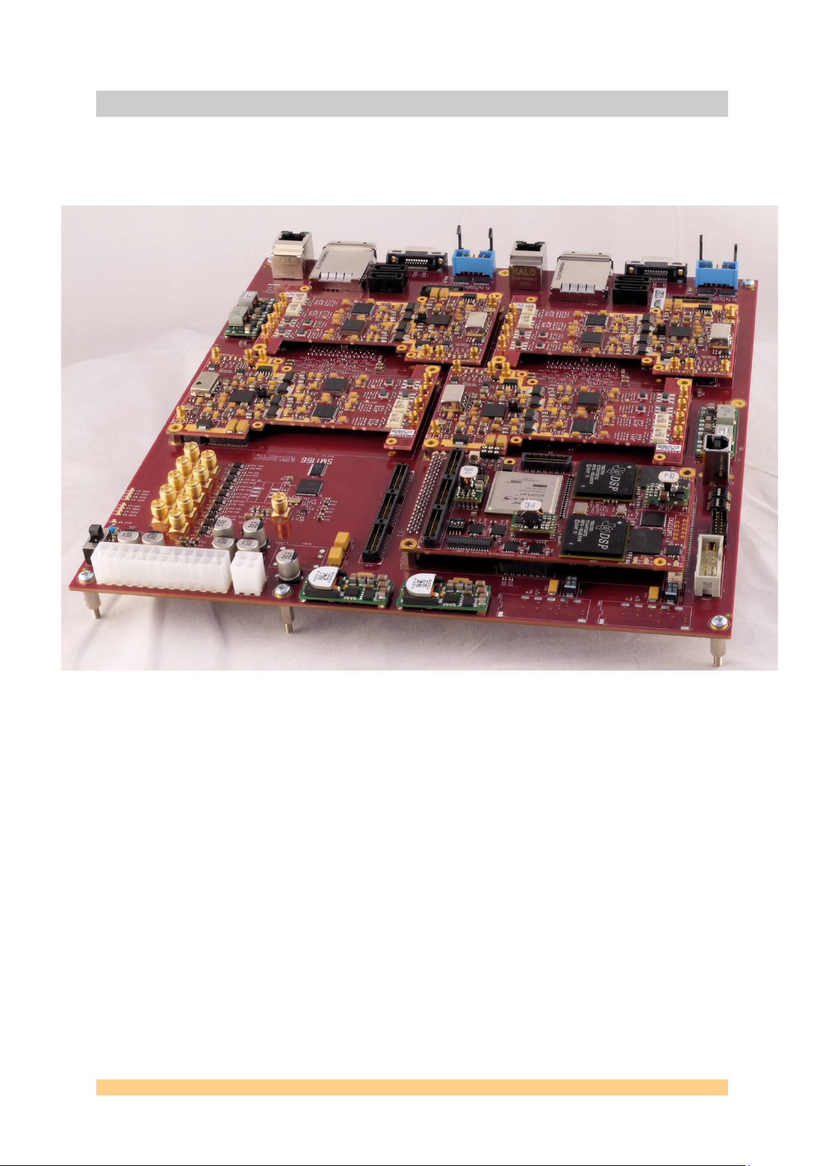
System Photograph
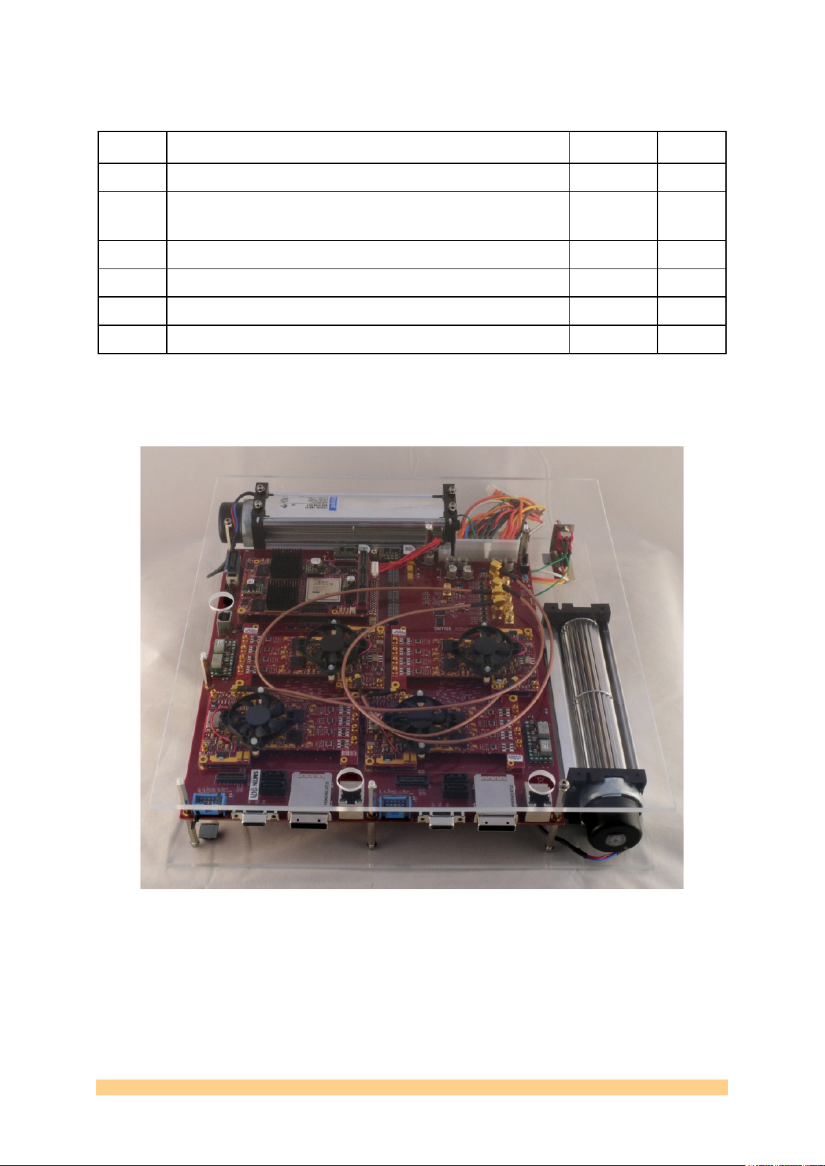
A typical system showing the SMT166 FPGA carrier board, four SMT943 quad ADCs, and an
SMT372T dual DSP TIM.
Product Specification SMT166 Page 7 of 44 Last Edited: 17/06/2014 16:12:00
Page 8
4
Functional Description
4.1
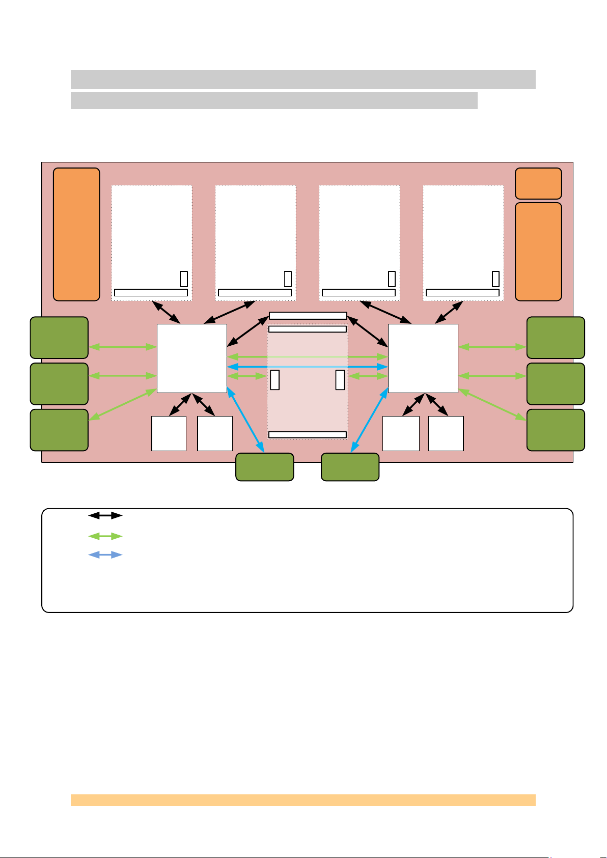
Block Diagram
SMT166
–
SLB Carrier Board
SLB Bus
Rocket IOs
Parallel Bus
An SLB cable can be used to link the SLB on the Master module to the SLB on the SMT
166 while using RSLs.
PCIe cable connectors can be used as a link to a host PC. 4 and 1-
lane cables are available as well as Host Interface Board to communicate to a
PC
.
FPGA_0
Virtex
6
LX
130
T-
LX
365T
SX315
T
-SX
475T
PSU
Section
DDR3
Memory
Bank 2
SLB
Mezzanine 0
SLB
SLB
Mezzanine 1
SLB
SLB
Mezzanine 2
SLB
SLB
Mezzanine 3
SLB
FPGA
_1
Virtex 6
LX130T-LX365T
SX315T-SX475T
DDR3
Memory
Bank
3
DDR3
Memory
Bank 0
DDR3
Memory
Bank 1
Full
SLB
i
Full SLB
j
Full
SLB
l
Full SLB
k
RSL x2
m
RSL x
2
n
Half SLB
n
Half SLB
m
RSL x4
o
i
Channels x2
PCIe
Cable
x4
x4
l
Master
Module
SLB Connector
R
S
L
R
S
L
PCIe
Cable
x
4
x
4
j
PCIe
Cable
x1
x
1
i
PCIe
Cable
x1
x1
k
USB+
CPLD
+Flash
To configure
Virtex6
FPGAs and
access
Master
Module Flash
Clock
Synthesiser
Synchroniser
Top TIM Connector
Bottom TIM Connector
Dual
SATA3.0
x
2
q
Dual
SATA3
.0
x2
p
1Gigabit
Ethernet
1
Gigabit
Ethernet
Figure 1 - SMT166 Block Diagram.
Below is shown the block diagram of the SMT166 board:
Product Specification SMT166 Page 8 of 44 Last Edited: 17/06/2014 16:12:00
Page 9
The tables below detail the SLB, RSL and Channel links:
SLB Links
i
j
k
l
m
n
RSL Links
i
lane express
j
lane express
k
lane express
l
lane express
m
n
o
Channel Links
i
bit bus (unidirectional), a clock, a
Two channels are between the FPGA0 and
Full SLB between FPGA0 and SLB site 0.
Full SLB between FPGA0 and SLB site 1.
Full SLB between FPGA1 and SLB site 2.
Full SLB between FPGA1 and SLB site 3.
Half SLB between FPGA0 and extra SLB connector.
Half SLB between FPGA1 and extra SLB connector.
Gen1 x1 express link between FPGA0 and 1connector. Also carries a reference clock and a reset.
Gen1 x4 express link between FPGA0 and 4connector. Also carries a reference clock and a reset.
Gen1 x1 express link between FPGA1 and 1connector. Also carries a reference clock and a reset.
Gen1 x4 express link between FPGA1 and 4connector. Also carries a reference clock and a reset.
x2 RSL link between FPGA0 and Master module.
x2 RSL link between FPGA1 and Master module.
x4 RSL link between FPGA0 and FPGA1.
One channel is defined as a 32write and a ready signal.
FPGA1.
Product Specification SMT166 Page 9 of 44 Last Edited: 17/06/2014 16:12:00
Page 10

4.2
Module Description
4.2.1
Connectors available on the board
4.2.1.1 SLB connectors and cables
The mounting posts and securing bolts for the SLBs and TIM are at 3.3V NOT GND.
SLB sites can receive SLB mezzanine modules. Connections are made via power and
data SLB connectors (Samtec connectors).
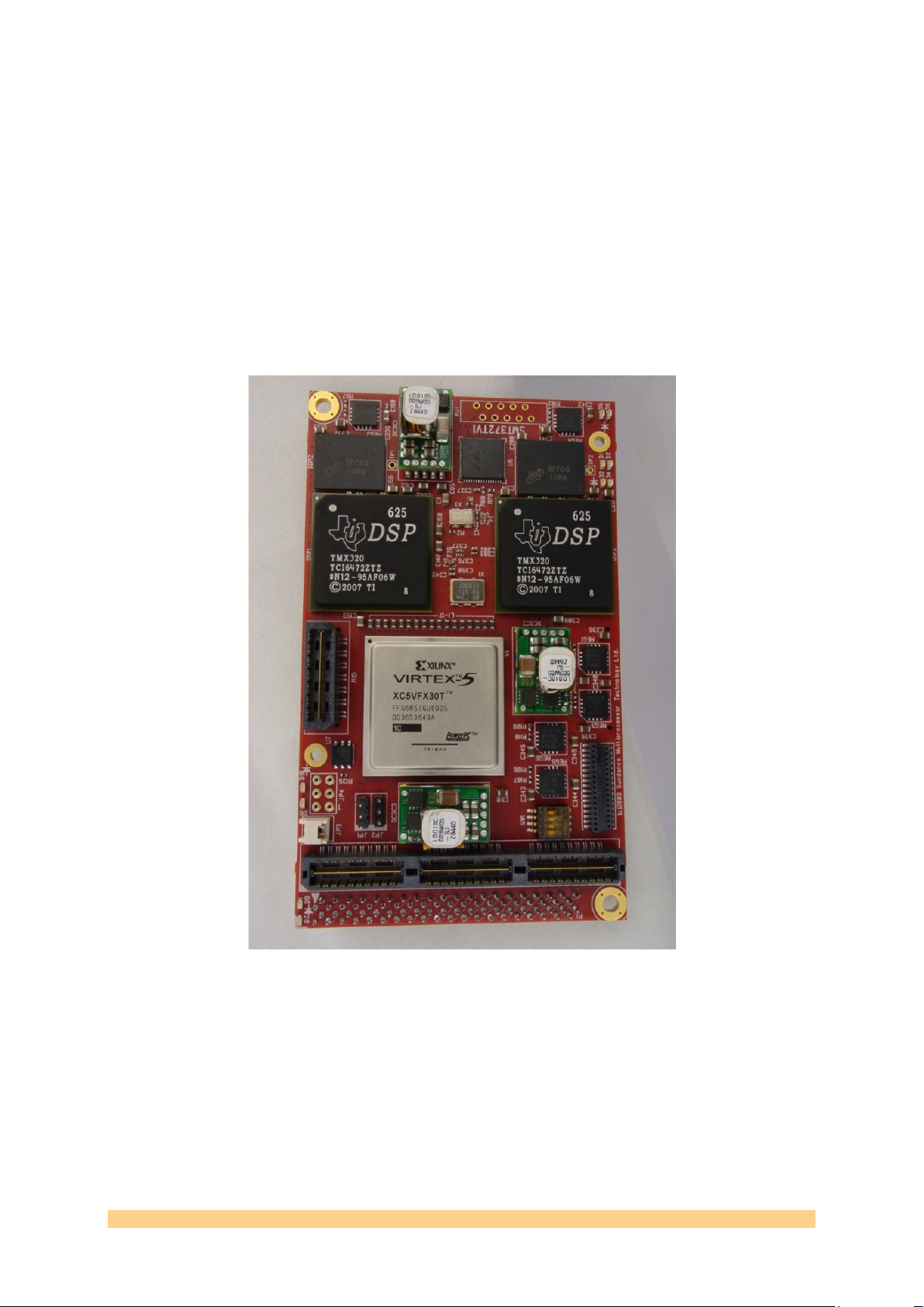
Shown below is an example SLB module. This is the SMT909 composite video input
module.
A fifth SLB data connector is available (not coupled with a power connector). Half of
the IOs are connected to the first FPGA and the second half to the second FPGA.
They can be used as general purpose IOs or be connected to the Master Module by
using an SLB cable.
Product Specification SMT166 Page 10 of 44 Last Edited: 17/06/2014 16:12:00
Page 11
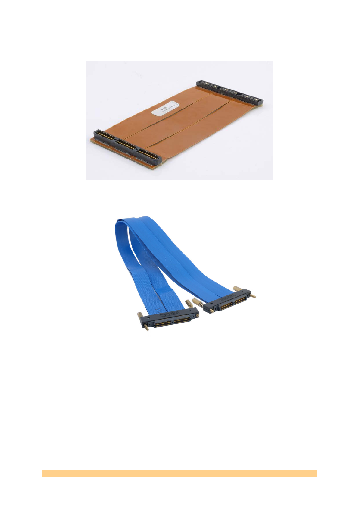
Two types of cable are available: flexiPCB type and blue ribbon cable type (shown
Figure 2 - SLB cable - FlexiPCB.
Figure 3 - SLB cable - Blue ribbon cable.
below).
Product Specification SMT166 Page 11 of 44 Last Edited: 17/06/2014 16:12:00
Page 12
4.2.1.2 TIM Site
A TIM site (Texas Instruments Module) is provided adjacent to the fifth SLB
connector. The positioning of these two allows a simple 1-1 cable connection from
th
the 5
SLB connector directly to the SLB connector on the TIM (where available).
Other connections from the TIM site are a ComPort connection to the USB interface,
RSL connections to both Virtex 6 FPGAs, and a JTAG connection allowing for
debugging using Code Composer Studio.
An example TIM is shown below. This is the SMT372T which has twin 6-core DSP
devices.
Product Specification SMT166 Page 12 of 44 Last Edited: 17/06/2014 16:12:00
Page 13
4.2.1.3 External clocks
4.2.1.4 PCI Express
Figure 4 - PCIe cables.
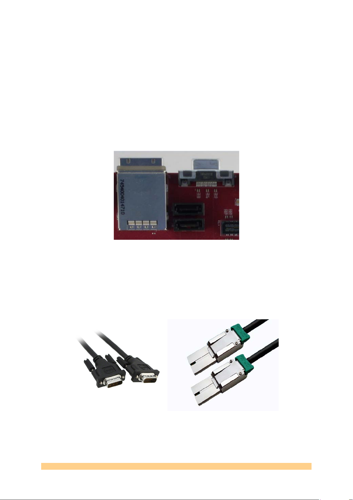
One External clock and one reference are fed to the board via MMCX connectors
(Huber-Suhner). They can be used to synchronise the on-board optional clock
circuitry to an external system clock domain.
PCI Express (x1 and x4) connectors are horizontal connectors (female) and
manufactured by Molex. Connections between 2 boards or between one board and a
host can be implemented using a male-male PCI Molex cable.
FPGAs populated on the SMT166 features two PCI Express blocks, which means that
both express interfaces can be used simultaneously.
The SMT166 will receive a Gen1 PCI Express core (Endpoint with Link speed of
2.5Gbits/s and user clock of 125MHz) but has the capabilities of receiving a Gen2
version of the core (Endpoint with Link speed of 5GBits/s and user clock of
250MHz).
Typical cable examples are shown here:
The 4-lane Express core can be implemented using PCIE_X0Y1.
Product Specification SMT166 Page 13 of 44 Last Edited: 17/06/2014 16:12:00
Page 14
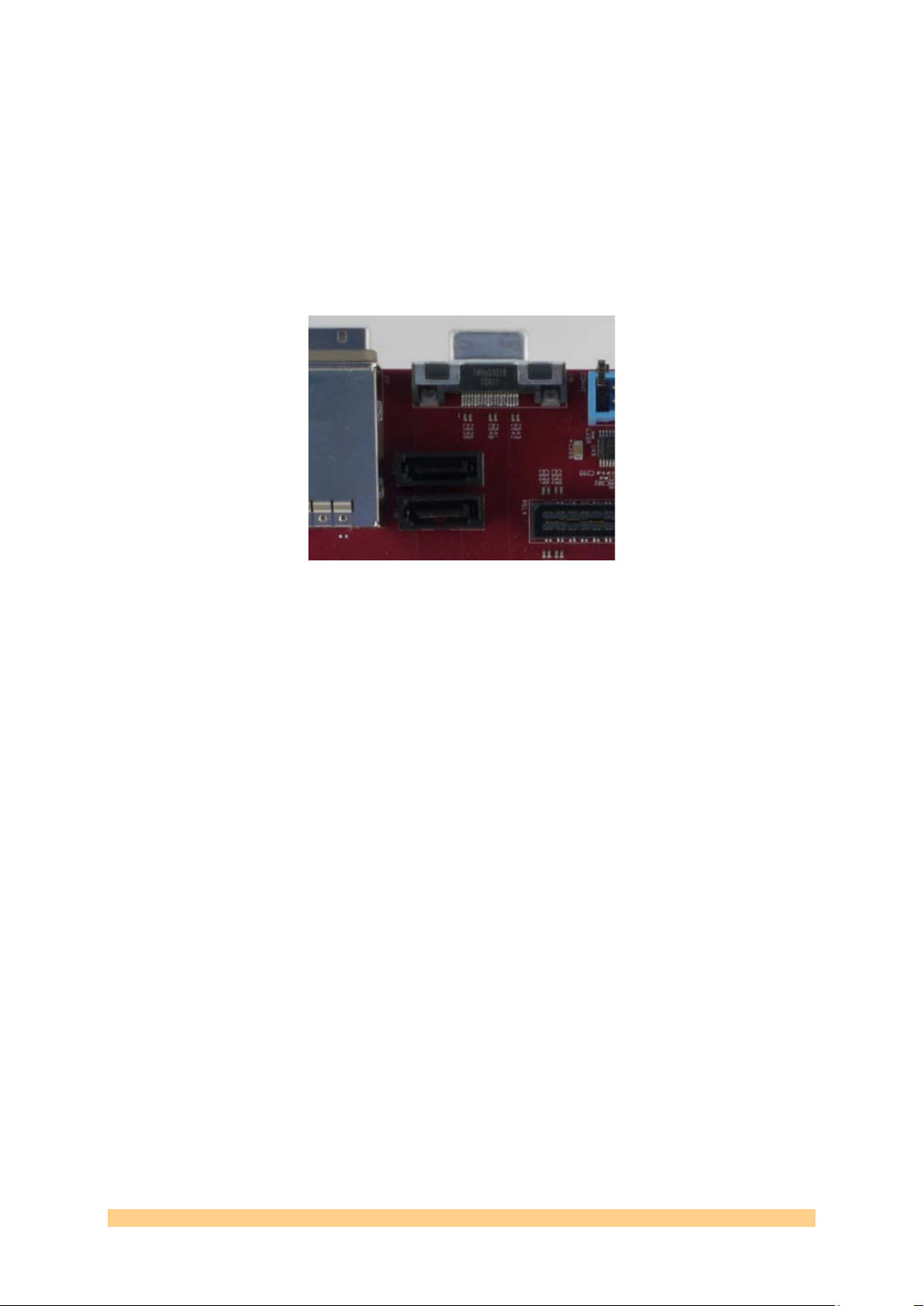
4.2.1.5 SATA 3.0
4.2.1.6 Ethernet
4.2.1.7 RS232 headers
This 10-pin header is NOT directly compatible with a standard PC COM port.
Two SATA3.0 connectors are available per FPGA.Virtex-6 Rocket IOs have got the
ability to be configured as 3Gbit/s or 6Gbit/s SATA links.
Virtex6 rocket IOs a connected in direct, which means that the FPGA acts as a host
and can write or read to/from a connected hard disk.
Links between 2 boards would require cross-over SATA cables.
Optionally, the SMT166 can receive a 1-gigabit Ethernet connector. Xilinx has made
available a 1-gigabit Ethernet core that can be implemented in a Virtex6 and using a
TEMAC block. A purchased license might be required in order to get full capabilities
of the core.
The RS232 will have simple 2mm header. A custom made cable is required for
connection to a host machine as each header contains 4 transmit and 4 receive
signals.
Product Specification SMT166 Page 14 of 44 Last Edited: 17/06/2014 16:12:00
Page 15

4.2.1.8 Power supply
Figure 5 - ATX Power connectors.
The 4-pin socket adjacent to the 24-pin ATX connector (if fitted) should only be
used to power fans and other peripherals. It should not be used for connection to
an ATX 12V power source.
The board can be powered using just the 24-pin ATX connector. Alternatively, the
whole board can be powered using just the +12V input pins on the secondary 4-pin
connector and/or the +12V pins on the 24-pin connector. This is a build-time
option.
This is the only power supply to the board. All other power rails going to all 5 sites
as well as all the components mentioned in this document are derived from the
+12V rail.
Product Specification SMT166 Page 15 of 44 Last Edited: 17/06/2014 16:12:00
Page 16

4.2.2
FPGAs
4.2.2.1 FPGA Power supplies
FPGA
Quiescent
Vccint
(amps)
Quiescent
Vccaux
(amps)
LX130T
LX195T
LX240T
LX365T
SX315T
SX475T
Figure 6 - FPGA power requirement.
Virtex6 FPGAs offer good features for this design such as high-performance logic, a
great number of IOs per package, the capability of driving some DDR3 memory, PCI
Express endpoints, GTX transceivers for serial connectivity, LVDS IOs, built-in
memory blocks, internal clock managers and integrated TEMACs.
The SMT166 features two Virtex6 FPGAs in an FF1156 package that can be LX130T,
LX195T, LX240T, LX365T, SX315T or SX475T. All parts are footprint compatible.
FPGAs have got their internal core powered at 1.0 Volt (Vccint). IOs will be powered
under 3.3, 2.5 or 1.5 Volts (Vcco). Below are shown the quiescent currents for each
part.
1.6 0.08
2.0 0.12
2.4 0.14
3.0 0.19
3.5 0.20
5.2 0.28
We can estimate that each FPGA core (Vccint) could require up to 16Amps. The
auxiliary (Vccaux) rail is likely to take up to 2 Amps.
DDR3 IOs can be powered by from the DDR3 main supply and only driving outputs
are drawing current.
A 20-amp power module for each FPGA Core voltage should be sufficient to cover
all needs.
There are 3 speed grades available, -1, -2 and -3 (fastest). The SX475T is not
available in the -3 speed grade (as of Nov 2011).
Product Specification SMT166 Page 16 of 44 Last Edited: 17/06/2014 16:12:00
Page 17

4.2.2.2 FPGA Clock structure
4.2.2.3 FPGA Configuration
FPGA
Bitstream size
Virtex6 LX130T
Virtex6 LX195T
Virtex6 LX240T
Virtex6 LX365T
Virtex6 SX315T
Virtex6 SX475T
Figure 7 - FPGA Bitstream sizes.
SLB connectors show 4 LVDS clock lines (that’s 2 per SLB data bank). Xilinx Global
clock buffers can’t be used as there are simple not enough in the chip. Virtex6
FPGAs offer an alternative via the Regional Clock buffers. All clock lines coming
from the SLB connector are mapped to a Clock Capable pin, which allows connection
to BUFRs (Multi-Regional clock buffers). Each SLB has been assigned an FPGA pinout
made out of consecutive IO banks, which means that any SLB clock can be used to
latch in/out data lines anywhere from/to anywhere on the connector
Similarly, both parallel channels between the FPGAs have their clocks mapped on
multi-regional clock buffers.
Only the on-board clock is connected to Global Clock Buffer pads on the FPGAs.
System clocks required:
- 100-MHz general purpose clock (can be used for registers, RS232, etc),
- 200-MHz for the TEMAC interface (Coregen),
- 300-MHz for DDR3 idelay controller (DDR3 interface - Coregen),
- 400-MHz DDR3 clock (effectively clocks the DDR3 memory – defines the read
and write throughputs).
Alternatively, the clock coming out of one of the PCI Express cores can be used to
clock other interfaces and ensure a synchronisation in frequency and avoiding
crossing clock domains.
Both FPGAs and CPLD can be programmed through the JTAG chain via a Xilinx
programming cable. FPGA configuration being volatile, the operation has to be done
again after each power off. The location of the Xilinx JTAG header is shown in
section 10.
Bitstreams can be stored into Flash Memory accessible from a host PC/unit via a
USB2.0 connection.
The SMT166 can be populated with FPGA ranging from the LX130T up to the
LX395T (all based on the same physical package).
Below is a table gathering sizes of bitstreams for each FPGA
43.8 Mbits
61.6 Mbits
73.9 Mbits
96.1Mbits
104.5Mbits
Product Specification SMT166 Page 17 of 44 Last Edited: 17/06/2014 16:12:00
156.7Mbits
Page 18

The onboard flash used can contain up to 4 bitstreams for a 512 Mbit flash and up
SMT166 – Configuration
FPGA_0
Virtex 6
LX130T-LX395T
FPGA_1
Virtex 6
LX130T-LX395T
Flash
USB2.0
CPLD
Mode selection
made via
switches
Config
.
Port
Configuration Port
Comport
3
Master Module
JTAG
Figure 8 - Configuration Block Diagram.
to 8 for a 1Gbit flash, which is divided into equal 128Mbit regions. As standard a
512Mbit device is fitted. This is sufficient for two bitstreams for any size FPGA.
The SMT6002 software takes care about generating the correct offset/address while
writing bitstreams. The first bitstream should be stored at address 0x0 in the flash
and the second at address 0x200,0000, in order for the biggest/first bitstream to fit
without overlapping on the second bitstream.
Below is a block diagram showing the connections between FPGAs, CPLD and Flash:
Product Specification SMT166 Page 18 of 44 Last Edited: 17/06/2014 16:12:00
Page 19

4.2.3
DIP Switch Settings / FPGA Configuration
SW3
SW2
Function
When the board is powered up or the reset button pressed, the CPLD performs the
process of configuring the FPGAs. There are several options available as decided by
the DIP switch settings. These switches are located as shown here:
The following table shows the settings available:
1 2 3 4 1 2 3 4
On Off Off Off On On Off Off SMT166 flash programming
Off Off Off Off On On Off Off TIM flash programming
Off Off Off Off On On On On Normal operation
The first setting (SMT166 flash programming) is used when the flash is required to
be programmed with FPGA bitstreams using Sundance’s SMT6002 flash
programming software package.
The second setting (TIM flash programming) allows the SMT6002 package to be able
to program the flash on the attached TIM (if present. See TIM user guide for details).
Product Specification SMT166 Page 19 of 44 Last Edited: 17/06/2014 16:12:00
Page 20

The last setting (Normal operation) allows the CPLD to configure the FPGAs from
bitstreams stored in flash.
Product Specification SMT166 Page 20 of 44 Last Edited: 17/06/2014 16:12:00
Page 21

4.2.4
DDR3 Memory
The SMT166 has got four independent DDR3 memory banks. Each Virtex6 FPGA is
responsible for providing access to two banks. Memory chips used are
manufactured by Micron and can be clocked at up to 666MHz (DDR3-1333). In a
more reasonable approach, a 400MHz memory clock will allow storing 3.2Gbytes/s
and per bank. For power consumption reasons, the clock frequency is brought
down.
-1 speed grade FPGA will only allow the DDR3 interfaces to work at 400MHz. Fitting
a -2 and -3 FPGA will give access to the full speed of 533MHz. The limitation here is
the FPGA.
Each memory bank is 32-bit wide and made out of 2 memory chips (MT41J64M16xx15E – 2Gbit part) and can store up to 256 Mbytes of data. Memory chips are
powered under 1.5 Volts (Vdd and Vddq) and can take up to 430mA each. The board
counts in total 16 chips, giving a total of nearly 7Amps.
This image shows the Virtex-6 FPGA and its two associated DDR3 memory banks
(two devices per bank).
DDR3 memory also requires a reference voltage (half of the supply voltage,
Vrefdq=0.75 Volt). The current required for the reference level is negligible
compared to the supply voltage but must coming from a sink/source regulator.
14mA per chip gives a total of 224mA.
The FPGAs will use their internal reference voltage, derived from the FPGA bank
power supply (Vcco). Active terminations are also used on the FPGA (DCI) and can
be cascaded from one bank to another (Xilinx User Constraint File).
To cover the need of all DDR3 banks and the FPGA IOs, a 16-amp power module is
used.
Product Specification SMT166 Page 21 of 44 Last Edited: 17/06/2014 16:12:00
Page 22

4.2.5
On-board reset
4.2.6
Clock circuitry (optional)
A push button is dedicated to reset the board, and clear and reload the FPGA
configuration. It is coupled with a reset chip in order to avoid multiple resets.
The reset signal only goes to the CPLD. The CPLD then propagates the reset signal to
the FPGAs and other peripherals such as the USB circuitry.
The button is located as shown below – bottom left.
The optional clock circuitry is built around a CDCE72010 from Texas Instrument. It
is a clock synchroniser, jitter cleaner and clock distributor.
When coupled with a VCXO, it can be locked to a reference signal and generate
synchronised in phase and frequency outputs, which can then be used on SLB
mezzanine modules present on the SMT166.
The clock chip requires programming through its serial interface port. Serial lines
are connected to the first FPGA.
The clock circuitry is physically isolated from the rest of the board in order to
reduce potential electrical disturbances.
Product Specification SMT166 Page 22 of 44 Last Edited: 17/06/2014 16:12:00
Page 23

4.2.7
General purpose IOs
4.2.8
RS232
Signal
Pin #
Pin #
Signal
4.2.9
USB
4.2.10 Ethernet
The extra SLB connector present on the SMT166 can be used as general purpose IOs.
SLB signals can be 2.5 or 3.3 Volts. This selection is made via jumpers.
Other general purpose IOs can be added by the way of the Master Module site. For
instance an SMT372T placed on the site could have its SLB also dedicated for such
use.
Two RS232 connections are available on the SMT166. There is one for each FPGA.
The pin-out is shown here:
RX0 1 6 TX0
RX1 2 7 TX1
RX2 3 8 TX2
RX3 4 9 TX3
GND 5 10 GND
The FPGA pin numbers can be matched with the above signal names.
The physical layout of the connector is the same as shown above. It is not
compatible with a standard PC 9-pin D-sub.
A USB interface is available to the CPLD for communication to and from a host. This
is to be used for read and write operation in the flash.
Virtex6 FPGA features built-in TEMAC blocks. There are 4 per FPGA. One will be
dedicated to communicate to an external PHY. This 1-gigabit Ethernet can be used to
connect to a remote host to receive or send commands and/or collect or send data
for storage as an example.
Note that some license might need to be acquired prior to implementing the core
provided by Xilinx.
Product Specification SMT166 Page 23 of 44 Last Edited: 17/06/2014 16:12:00
Page 24

4.2.11 SATA3.0
4.2.12 RSLs to Master module
4.2.13 Inter-FPGA RSL links
4.2.14 Inter-FPGA channels
Xilinx FPGAs such as the Virtex6 have got Rocket IOs that can be configured as
3Gbit/s SATA links (URL:SATA HOST IP
order to implement a full SATA3.0 link.
). A license for a full core will be required in
Two RSL lanes are available between each Virtex6 FPGA and one RSL connector on
the Master Module. RSL can sustain transfers at 200Mbytes/s per lane.
Communication between FPGAs can be made via RSLs. Four are available between
FPGAs. Standard Sundance RSLs can achieve in excess of 300Mbytes/s per lane.
Virtex6 technology allows even faster rates so a transfer rate of 600Mbytes/s per
lane could be achieved.
Lanes are crossed-over on the PCB in order to have two identical firmware able to
exchange data via RSLs.
A Channel is known as a parallel bus for transferring data. Being a parallel bus (as
opposed to serial) avoids un-deterministic latency due to FIFO and encoding,
generally used in serial transfer cores.
Sundance channels are not tied to a specific clock rate. Recently channels have been
successfully used at 250MHz, in DDR mode, meaning that transfer rate of up to
2Gbytes/s per channel can be achieved.
Two channels are implemented between the FPGAs.
Product Specification SMT166 Page 24 of 44 Last Edited: 17/06/2014 16:12:00
Page 25

4.2.15 LEDs
Eight LEDs are connected to the Virtex 6 FPGAs. They are located as shown here:
The top 4 are connected to FPGA0 and the bottom 4 to FPGA1.
The FPGA pins used to control these LEDs are given in section 11.
Product Specification SMT166 Page 25 of 44 Last Edited: 17/06/2014 16:12:00
Page 26

4.3
Cooling of the board
Figure 9 - Crossflow blower.
Elements on the board such as the memory, power supplies, CPLD should not
require any specific cooling solutions. When it comes to the FPGAs, by the amount
of current it can draw and the logic they can implement, they will require a cooling
solution.
Xilinx ISE software can be of great to evaluate the size of the heat sink or fan. It
indeed incorporates a power estimator that can be run from an existing FPGA
design. This operation will take place at a later stage and also to validate the FPGA
pinout.
In the mean time, we could think of a solution based on crossflow blowers. A couple
could be used instead of metal stand-off (pillars) to rest the board and blowing
towards the FPGA, which could also receive a high-efficiency heat sink (fins).
It is recommended that the supplied enclosure (if purchased) be used for
development. This includes two crossflow blowers which are required to keep the
operating temperatures of the Virtex 6 FPGAs within their operational ranges.
Product Specification SMT166 Page 26 of 44 Last Edited: 17/06/2014 16:12:00
Page 27

4.4
Data Flow Block Diagram
SMT166
– SLB Carrier Board
FPGA
_
0
Virtex 6
LX130T-LX365T
SX315T-SX475T
PSU
Section
DDR
3
Memory
Bank 2
4Gbytes/s
SLB
Mezzanine
0
SMT941
SLB
SLB
Mezzanine 1
SMT941
SLB
SLB
Mezzanine
2
SMT941
SLB
SLB
Mezzanine
3
SMT941
SLB
FPGA
_
1
Virtex
6
LX130T-
LX365
T
SX315
T-SX475
T
DDR
3
Memory
Bank
3
4Gbytes/
s
DDR
3
Memory
Bank 0
4
Gbytes/s
DDR3
Memory
Bank
1
4Gbytes/s
2 Gbytes/s
2
Gbytes
/
s
2 Gbytes/s
2
Gbytes
/
s
400
Mbytes
/s
400
Mbytes/s
800
Mbytes
/s
2
x 2Gbytes
/s
PCIe
Cable
x
4
800
Mbytes
/
s
Master
Module
SLB Connector
R
S
L
R
S
L
PCIe
Cable
x
4
800
Mbytes
/s
PCIe
Cable
x
1
200
Mbytes/
s
PCIe
Cable
x
1
200 Mbytes/s
USB
+
CPLD
+
Flash
To configure
Virtex6
FPGAs and
access
Master
Module Flash
Clock
Synthesiser
Synchroniser
Top TIM Connector
Bottom TIM Connector
Dual
SATA
3.0
500
Mbytes
/s
Dual
SATA
3.0
500
Mbytes
/
s
Figure 10 - Data Flow Diagram.
Below is shown the block diagram of the board on a data flow point of view and also
showing some of the maximum transfer speed achievable:
The example shown in the above data flow block diagram has been elaborated with
four SMT941s in mind (one of the fastest SLB mezzanine modules within Sundance’s
range with a 2Gbytes/s output rate). SLB data flow can remain ‘local’ and be
processed or stored by the FPGA they are connected to, or be rerouted to the other
FPGA without a slowing down in speed (using channels).
Once stored and processed, data can be transferred at a slower rate to a host.
Product Specification SMT166 Page 27 of 44 Last Edited: 17/06/2014 16:12:00
Page 28

4.5
SLB IO voltages
Virtex6 FPGAs don’t allow 3.3 Volts on the IO pins, only 2.5 Volts.
SLB mezzanine Module
IO Voltage required
IO converter board
required
SMT350
SMT381
No
SMT384
SMT390
SMT391
No
SMT399-190
SMT901
SMT911
SMT903
SMT909
No
SMT916
No
SMT939
No
SMT941
No
SMT942
No
SMT943
No
SMT950
SMT959
No
Figure 11 - SLB Selection
green
Sundance SLB mezzanine modules show different signalling voltages. Control and
data signals can be either 2.5 Volts or 3.3 Volts. So far, Sundance SLB base modules
allow the IO voltage selection.
2.5-V SLB mezzanine modules can be used/plugged directly on the SMT166 carrier
board. When it comes to the 3.3-V SLB mezzanines, an IO converter board has to be
purchased from Sundance. The table below shows the voltages of all SLB mezzanine
modules produced by Sundance:
3.3 Volts Yes
2.5 Volts
3.3 Volts Yes
3.3 Volts Yes
2.5 Volts
3.3 Volts Yes
3.3 Volts Yes
3.3 Volts Yes
3.3 Volts Yes
2.5 Volts
2.5 Volts
2.5 Volts
2.5 Volts
2.5 Volts
2.5 Volts
3.3 Volts Yes
2.5 Volts
Modules highlighted in
without any voltage converter board required.
Product Specification SMT166 Page 28 of 44 Last Edited: 17/06/2014 16:12:00
above are directly compatible with the SMT166
Page 29

5
Verification, Review and Validation Procedures
6
Safety
7
EMC
8
Timing Diagrams
To be carried out in accordance with the Sundance Quality Procedures (ISO9001).
See: http://www.sundance.com/web/files/static.asp?pagename=quality
This module presents no hazard to the user when in normal use.
This module is designed to operate from within an enclosed host system, which is
build to provide EMC shielding. Operation within the EU EMC guidelines is not
guaranteed unless it is installed within an adequate enclosure.
This module is protected from damage by fast voltage transients originating from
outside the host system which may be introduced through the output cables.
Short circuiting any output to ground does not cause the host PC system to lock up
or reboot.
TBA
Product Specification SMT166 Page 29 of 44 Last Edited: 17/06/2014 16:12:00
Page 30

9
Circuit Description / Diagrams
9.1
Clock circuitry:
The circuits below are of the main elements within the design. Full schematics can
be made available upon request and to selected partners.
Product Specification SMT166 Page 30 of 44 Last Edited: 17/06/2014 16:12:00
Page 31

9.2
CPLD and FPGA configuration:
9.3
DDR3 Memory:
Product Specification SMT166 Page 31 of 44 Last Edited: 17/06/2014 16:12:00
Page 32

9.4
RS232:
9.5
RSL:
Product Specification SMT166 Page 32 of 44 Last Edited: 17/06/2014 16:12:00
Page 33

9.6
SLB:
9.7
SLB Aux Site:
Product Specification SMT166 Page 33 of 44 Last Edited: 17/06/2014 16:12:00
Page 34

9.8
TIM Site:
9.9
USB:
Product Specification SMT166 Page 34 of 44 Last Edited: 17/06/2014 16:12:00
Page 35

9.10
Inter-FPGA Channels:
Product Specification SMT166 Page 35 of 44 Last Edited: 17/06/2014 16:12:00
Page 36

10
Layout
Figure 12 - PCB Layout.
The layout shown below provides the locations of the major components of the
board (exact positions are subject to change). Red pads mean that the component is
placed on the top layer and blue on the bottom layer.
The board size is 266 x 250mm.
Product Specification SMT166 Page 36 of 44 Last Edited: 17/06/2014 16:12:00
Page 37

11
Pinout
Interface
Signal / Bus
FPGA Pin #
CS:J17 RAS:L14 CAS:B16 WE:F16 CKE:E16
Interface
Signal / Bus
FPGA Pin #
AP16 AJ16 AJ17 AM15 AN15 AF16 AG16 AL14
AL10 AG11 AG10 AJ10 AH10 AC12 AD11 AP12
AN12 AE14 AF14 AN13 AM13 AK13 AL13 AH13
CS:AJ19 RAS:AD16 CAS:AC17 WE:AH18
CKE:AN17 ODT:AP17 CKP:AC15 CKN:AD15
AD14/AC14 AL11/AM11 AG12/AH12
Interface
Signal / Bus
FPGA Pin #
DDR3 Bank A Addr[0:14] M18 J19 K19 B17 C17 L18 L19 G17 H17 K17 K18
All I/O are 1.5V with internal Vref. DCI cascade Master:35 Slave:36
D17 E18 E17 F18
Data[0:31] J16 A15 B15 G15 F15 H15 J15 D15 G13 H14 G11
F11 A13 A14 G12 H13 E14 H10 G10 K14 J14 M13
M11 C12 J12 A11 B11 J11 J10 D12 E12 K13
BA[0:2] L15 H18 M17
Control
ODT:D16 CKP:K16 CKN:L16 RESET:G16
DM[0:3] C15 F14 H12 K12
DQSP/N[0:3] M16/M15 D14/C14 B12/B13 E13/F13
DDR3 Bank B Addr[0:14]
AL15 AH15 AJ15 AJ14 AK14 AF15 A?G15
Data[0:31] AE13 AE12 AJ11 AK11 AK12 AJ12 AF11 AE11
AH19 AM17 AM16 AD17 AE17 AE18 AF18 AL16
BA[0:2] AE16 AG17 AP15
Control
RESET:AG18
DM[0:3] AM10 AM12 AH14 AK16
DQSP/N[0:3]
AK18/AK17
All I/O are 1.5V with internal Vref. DCI cascade Master:33 Slave:32
Flash D[0:7] AF24 AF25 W24 V24 H24 H25 P24 R24
Product Specification SMT166 Page 37 of 44 Last Edited: 17/06/2014 16:12:00
Page 38

Interface
Signal / Bus
FPGA Pin #
SLB0 DAIP/N[0:7]
C20/D20 G21/G22 J20/J21 E22/E23 F19/F20
A23/A24 B23/C23 B21/B22 A20/A21 H19/H20
C32/B32 E32/E33 A33/B33 C33/B34 D34/C34
J26/J27 F30/G30 G31/H30 K28/J29 F31/E31
B27 D24 C28 C29 F25 G27 C27 E24 B28 D29
SerNum:C25 PSEN0:D27 PSEN1:E27 MODE0:B26
DBIP/N[0:7]
DAQP/N[0:7]
DBQP/N[0:7]
CKOUTIP/N B20/C19
CKOUTQP/N F21/G20
RSLCLKP/N K26/K27
SYSCLKP/N F33/G33
DooRIP/N L20/L21
DooRQP/N L25/L26
ExtTrigIP/N C22/D22
ExtTrigQP/N J31/J32
SIGNAL[0:11] G26
D21/E21 H22/J22 K21/K22
E19/D19 A18/A19 B18/C18
E34/F34 H34/H33 K33/J34
J30/K29 D31/D32 G32/H32
G25
CNTRL[0:8] E26 B25 F26 A25 H27 A28 F28 G28 A29
SMB CLK:D25 DATA:D26 ALERT:C24
Misc
DooR is Data out of Range.
Two independent channels I and Q.
MODE1:A26
Product Specification SMT166 Page 38 of 44 Last Edited: 17/06/2014 16:12:00
Page 39

Interface
Signal / Bus
FPGA Pin #
SLB1 DAIP/N[0:7]
AL30/AM31 AN32/AM32 AL31/AK31 AJ29/AJ30
AP32/AP33 AM33/AL33 AK33/AK32 AJ31/AJ32
AN33/AN34 AL34/AK34 AJ34/AH34
AM18/AL18 AP19/AN18 AN19/AN20
AL28 AN28 AH25 AN27 AK27 AH23 AK28 AM28
AG25 AP30 AG26 AP31 AK26 AL26 AJ24 AJ26
SerNum:AH27 PSEN0:AL29 PSEN1:AK29
DBIP/N[0:7]
DAQP/N[0:7] AE21/AD21 AG22/AH22 AK22/AJ22 AC20/AD20
DBQP/N[0:7]
CKOUTIP/N AG27/AG28
CKOUTQP/N AF30/AG30
RSLCLKP/N AP20/AP21
SYSCLKP/N AK19/AL19
DooRIP/N AE27/AD27
DooRQP/N AG20/AG21
ExtTrigIP/N AD25/AD26
AF26/AE26 AH29/AH30 AF28/AF29 AE28/AE29
AH33/AH32
AF19/AE19 AJ20/AH20 AC19/AD19 AK21/AJ21
AM20/AL20 AF20/AF21 AM21/AL21 AM23/AL23
AM22/AN22
ExtTrigQP/N AP22/AN23
SIGNAL[0:11]
CNTRL[0:8]
SMB CLK:AM30 DATA:AN30 ALERT:AH28
Misc
DooR is Data out of Range.
Two independent channels I and Q.
AJ25 AM27 AJ27 AH24
AM26
MODE0:AN29 MODE1:AP29
Product Specification SMT166 Page 39 of 44 Last Edited: 17/06/2014 16:12:00
Page 40

Interface
Signal / Bus
FPGA Pin #
Half SLB DAP/N[0:7]
AA34/AA33 AD34/AC34 AC33/AB33 AA25/Y26
AA30/AA31 AB30/AB31 AE31/AD31
AA28/AA29 AD29/AC29 AB28/AC28
AD22 AC22 AC24 AC23 AE22 AE23 AB23 AA23
The Half SLB interface uses the Q data bus section for FPGA1 and the I section for
Interface
Signal / Bus
FPGA Pin #
M31 L31 N25 M25 K32 K31 M26 M27 P31 P30
Interface
Signal / Bus
FPGA Pin #
DBP/N[0:7]
CKOUTP/N AD30/AC30
CLKP/N AE33/AF33
DooRP/N AG31/AF31
ExtTrigP/N AB25/AC25
CNTRL[0:14]
FPGA2.
Channel 0 Data[0:31]
AE34/AF34 AB32/AC32 AD32/AE32 AG33/AG32
AB27/AC27 AA26/AB26
AG23 AF23 AA24 Y24 G23 H23 N24
N27 P27 L33 M32 L28 M28 P25 P26 R28 R27 R31
R32 R26 T26 K34 L34 M30 N30 N34 P34 P29 R29
Clock N28
Write N29
CE M33
Ready N33
Channel 1 Data[0:31] U25 T25 T28 T29 R33 R34 T30 T31 T33 T34 U26
U27 U33 U32 U28 V29 V32 V33 Y32 Y31 Y33 Y34
W29 Y29 W31 W32 Y28 Y27 W25 V25 W27 W26
Clock V30
Write W30
CE W34
Ready V34
Product Specification SMT166 Page 40 of 44 Last Edited: 17/06/2014 16:12:00
Page 41

Interface
Signal / Bus
FPGA Pin #
Ethernet TxD[0:3] E8 E9 B8 C8
Interface
Signal / Bus
FPGA Pin #
Interface
Signal / Bus
FPGA Pin #
Interface
Signal / Bus
FPGA Pin #
RxD[0:3] AD10 AC9 AK8 AL8
TXCLK K9
TXCTRL L9
RXCLK AH9
RXCTRL AJ9
MDC AD9
MDIO AE9
RESET A9
COMA A8
RS232 TX[0:3] AF9 AF10 AG8 AH8
RX[0:3] AN9 AP9 AN10 AP10
SYS CLOCK CLKP/N L23/M22
100MHz
LED LED[0:3] N23 F23 F24 L24
Product Specification SMT166 Page 41 of 44 Last Edited: 17/06/2014 16:12:00
Page 42

Interface
Signal / Bus
FPGA Pin #
PCIe 1-lane GTX GTXE1_X0Y7
Interface
Signal / Bus
FPGA Pin #
Reset F10
PCIe 4-lane GTX[0:3] GTXE1_X0Y15 Y14 Y13 Y12
Reset F9
Product Specification SMT166 Page 42 of 44 Last Edited: 17/06/2014 16:12:00
Page 43

12
Board Options
SMT166-ATX
SMT166-ATX-CLOCK
SMT166-12V
SMT166-12V-CLOCK
13
Physical Properties
Four options will be available:
-
circuitry is populated on the board.
-
optional clock circuitry is populated.
-
populated on the board.
-
circuitry is populated.
: The board is powered using an ATX power supply. No clock
: The board is powered using an ATX power supply. The
: The board using a single 12V source. No clock circuitry is
: The board using a single 12V source. The optional clock
Dimensions 250mm x 266mm
Weight 500g with no modules
Supply Current
Idle.
With no modules.
MTBF
+12V 700mA
+5V 1.25A
+3.3V 130mA
-5V 0
-12V 0
Product Specification SMT166 Page 43 of 44 Last Edited: 17/06/2014 16:12:00
Page 44

14
Safety
15
EMC
This module presents no hazard to the user when in normal use.
This module is designed to operate from within an enclosed host system, which is
build to provide EMC shielding. Operation within the EU EMC guidelines is not
guaranteed unless it is installed within an adequate host system.
This module is protected from damage by fast voltage transients originating from
outside the host system which may be introduced through the output cables.
Short circuiting any output to ground does not cause the host PC system to lock up
or reboot.
Product Specification SMT166 Page 44 of 44 Last Edited: 17/06/2014 16:12:00
 Loading...