

Page 1

USER GUIDE
FOR
P
P
Parallel Application from Rapid Simulation
All rights reserved. No part of this document may be reproduced, translated,
stored in a retrieval system, or transmitted, in any form or by any means,
electronic, mechanical, photocopying, recording or otherwise, without prior
A
A
Copyright © Sundance
written permission of the owner.
Note:
R
R
S
S
If this copy is no longer in use, return to sender.
Page 2
APPROVAL PAGE
Name Signature Date
Sundance Digital Signal Processing, Inc.
4790 Caughlin Parkway 233, Reno, NV 89519-0907, U.S.A.
email: sales@sundancedsp.com
Tel: +1 (775) 827-3103 www.sundancedsp.com
Page 3
DOCUMENT HISTORY
Date Changes Made Issue Initials
Versions to accompany PARS releases < 10.2 MA, SM
29-Jul-2008 Edits during testing of PARS 10.2 6.0 NN
In Progress Rewrite for PARS 11 11-WIP BV
Sundance Digital Signal Processing, Inc.
4790 Caughlin Parkway 233, Reno, NV 89519-0907, U.S.A.
email: sales@sundancedsp.com
Tel: +1 (775) 827-3103 www.sundancedsp.com
Page 4

LIST OF ABBREVIATIONS
Abbreviation Explanation
CP Communications Port
DSP Digital Signal Processor
FPGA Field Programmable Gate Array
NA Not Applicable
PC Personal Computer
PCB Printed Circuit Board
PCI Peripheral Component Interconnect
PMC PCI Mezzanine Card
PrPMC Processor PMC
RF Radio Frequency
RSL RocketIO Serial Link
SDB Sundance Digital Bus
SDRAM Synchronous Dynamic Random Access Memory
SHB Sundance High-speed Bus
TBD To Be Determined
TI Texas Instruments
XMC Switched Mezzanine Card
Sundance Digital Signal Processing, Inc.
4790 Caughlin Parkway 233, Reno, NV 89519-0907, U.S.A.
email: sales@sundancedsp.com
Tel: +1 (775) 827-3103 www.sundancedsp.com
Page 5

TABLE OF CONTENTS
1. PREFACE......................................................................................................................................................... 11
1.1. INTENDED AUDIENCE ................................................................................................................................11
1.2. RELATED DOCUMENTATION ......................................................................................................................11
1.3. TRADEMARKS ...................................................................................................................................... 11
2. INTRODUCTION TO PARS.......................................................................................................................... 12
2.1. OVERVIEW............................................................................................................................................. 12
2.1.1. What is PARS?..................................................................................................................................... 12
2.1.2. Features............................................................................................................................................... 13
2.1.3. Benefits ................................................................................................................................................13
2.2. REQUIREMENTS ................................................................................................................................... 13
2.3. DEVELOPMENT FLOW ........................................................................................................................14
2.4. WALKTHRU................................................................................................................................................ 16
3. MODEL DEVELOPMENT ............................................................................................................................ 34
3.1. OVERVIEW................................................................................................................................................ 34
3.1.1. How PARS works with a model ...........................................................................................................34
3.2. PREPARING FOR CODE GENERATION ..........................................................................................................35
3.2.1. Solver Configuration ...........................................................................................................................36
3.2.2. Hardware Implementation...................................................................................................................37
3.2.3. Summary .............................................................................................................................................. 37
3.3. HARDWARE PROFILE SELECTION ...............................................................................................................38
3.4. PARTITIONING ........................................................................................................................................... 39
3.4.1. Connections between subsystems ........................................................................................................39
3.4.2. Connections between processors .........................................................................................................39
3.4.3. Data Types for Connections ................................................................................................................ 42
3.5. ALLOCATING PROCESSOR RESOURCES ...................................................................................................... 43
3.6. PRE-BUILT TASKS ..................................................................................................................................... 44
3.6.1. DSP PB Tasks......................................................................................................................................44
3.6.2. FPGA PB Tasks ................................................................................................................................... 44
3.6.3. SCOM PB Tasks ..................................................................................................................................44
3.7. HOST TESTBENCH STRATEGY ....................................................................................................................44
3.8. GENERATING APPLICATIONS ...................................................................................................................... 44
3.8.1. Pre-Compiled Libraries.......................................................................................................................44
3.8.2. FPGA Processors in Designs .............................................................................................................. 44
3.9. RUNNING THE TEST BENCH........................................................................................................................ 45
3.10. RESTRICTIONS ........................................................................................................................................... 45
3.11. COMMON ISSUES........................................................................................................................................45
3.11.1. Loop Deadlock................................................................................................................................45
3.11.2. Out-of-order Deadlock ................................................................................................................... 45
3.11.3. Rate Deadlock................................................................................................................................. 45
4. PARS COMPONENT REFERENCE ............................................................................................................46
4.1. PARS CONTROL PANEL .............................................................................................................................. 46
4.1.1. Overview..............................................................................................................................................46
4.1.2. File Menu ............................................................................................................................................46
4.1.3. PARS Menu.......................................................................................................................................... 46
4.1.4. Tool Menu............................................................................................................................................ 46
4.1.5. Help Menu ...........................................................................................................................................46
4.2. DSP TASKS............................................................................................................................................... 46
Sundance Digital Signal Processing, Inc.
4790 Caughlin Parkway 233, Reno, NV 89519-0907, U.S.A.
email: sales@sundancedsp.com
Tel: +1 (775) 827-3103 www.sundancedsp.com
Page 6

4.2.1. Overview..............................................................................................................................................46
4.2.2. Mask Options.......................................................................................................................................46
4.2.3. GRT vs. ERT ........................................................................................................................................ 47
4.3. FPGA TASKS............................................................................................................................................ 47
4.3.1. Overview..............................................................................................................................................47
4.3.2. Mask Options.......................................................................................................................................47
4.3.3. Clock Domain Considerations............................................................................................................. 47
4.3.4. HDLCoder vs. Xilinx System Generator .............................................................................................. 47
4.4. PARS DIAMOND LIBRARY........................................................................................................................47
4.4.1. Overview..............................................................................................................................................47
4.4.2. Diamond Blockset................................................................................................................................ 47
4.4.3. Device Driver Tasks ............................................................................................................................47
4.4.4. DSP Tasks............................................................................................................................................ 48
4.4.5. FPGA Tasks.........................................................................................................................................48
4.4.6. SCOM Tasks ........................................................................................................................................ 49
4.5. DSP PRE-BUILT TASKS ............................................................................................................................49
4.5.1. Overview..............................................................................................................................................49
4.5.2. Usage................................................................................................................................................... 49
4.5.3. Template of a DSP PB Task ................................................................................................................ 49
4.5.4. CPBT Operation for DSP Tasks .......................................................................................................... 49
4.5.5. Bind Input Block .................................................................................................................................. 49
4.5.6. Bind Output Block ............................................................................................................................... 49
4.5.7. Examples .............................................................................................................................................50
4.6. FPGA PRE-BUILT TASKS ......................................................................................................................50
4.6.1. Overview..............................................................................................................................................50
4.6.2. Usage................................................................................................................................................... 50
4.6.3. Template of an FPGA PB Task............................................................................................................ 50
4.6.4. CPBT Operation for FPGA Tasks ....................................................................................................... 50
4.6.5. Examples .............................................................................................................................................50
4.7. SCOM WRAPPER TASKS...........................................................................................................................50
4.7.1. Overview..............................................................................................................................................50
4.7.2. Usage................................................................................................................................................... 50
4.7.3. Hierarchy of SCOM Task Wrappers.................................................................................................... 50
4.7.4. SCOM Task Table................................................................................................................................50
4.7.5. Deriving New Variants ........................................................................................................................ 50
4.7.6. Examples .............................................................................................................................................50
4.8. HARDWARE DESCRIPTION FILE ................................................................................................................. 50
4.8.1. Overview..............................................................................................................................................50
4.8.2. Sections (.m file based input)...............................................................................................................50
4.8.3. Model Based Input (.mdl file) .............................................................................................................. 51
5. PARS GENERATED CODE .......................................................................................................................... 52
5.1. PARS HIERARCHY.................................................................................................................................... 52
5.2. DSP TASKS ...............................................................................................................................................52
5.2.1. Structure ..............................................................................................................................................52
5.2.2. Files (Production)................................................................................................................................ 52
5.2.3. Variants ............................................................................................................................................... 52
5.3. FPGA TASKS ............................................................................................................................................ 52
5.3.1. Structure ..............................................................................................................................................52
5.3.2. Common Files...................................................................................................................................... 52
5.3.3. Scalar vs. Vector Inputs....................................................................................................................... 52
5.3.4. Files .....................................................................................................................................................52
5.4. PRE-BUILT TASKS ................................................................................................................................... 53
Sundance Digital Signal Processing, Inc.
4790 Caughlin Parkway 233, Reno, NV 89519-0907, U.S.A.
email: sales@sundancedsp.com
Tel: +1 (775) 827-3103 www.sundancedsp.com
Page 7

5.4.1. Overview..............................................................................................................................................53
5.4.2. Files .....................................................................................................................................................53
5.5. PARS CONFIGURATION FILE.....................................................................................................................53
5.5.1. Overview..............................................................................................................................................53
5.5.2. Diamond Configuration Block............................................................................................................. 53
5.5.3. Sections................................................................................................................................................53
5.6. PARS APPLICATION .............................................................................................................................54
5.6.1. General Behavior ................................................................................................................................ 54
5.6.2. Boot Progression ................................................................................................................................. 54
6. HARDWARE ................................................................................................................................................... 55
6.1. PARS TARGET HARDWARE ...................................................................................................................... 55
6.1.1. Types....................................................................................................................................................55
6.1.2. Pre-Condition Requirements ...............................................................................................................55
6.1.3. Sundance Hardware ............................................................................................................................ 55
6.1.4. VMetro Hardware................................................................................................................................ 55
6.1.5. 3rd Party Board Support ..................................................................................................................... 55
7. ADVANCED FEATURES............................................................................................................................... 56
7.1. TASK CONTROL/STATUS INTERFACE......................................................................................................... 56
7.1.1. Overview..............................................................................................................................................56
7.1.2. AB105 Protocol Module ......................................................................................................................56
7.1.3. Task IDs...............................................................................................................................................56
7.1.4. Taskstate Protocol ............................................................................................................................... 56
7.1.5. Operation under HIL ...........................................................................................................................56
7.1.6. Operation in Standalone (embedded) Systems ....................................................................................56
7.2. PROFILING INTERFACE............................................................................................................................... 56
7.2.1. Overview..............................................................................................................................................56
7.2.2. PARS-Profile Module .......................................................................................................................... 56
7.2.3. Profile Report ...................................................................................................................................... 56
7.2.4. Operation under HIL ...........................................................................................................................56
7.2.5. Operation in Standalone (embedded) Systems ....................................................................................56
7.3. DEBUGGING (LOG) INTERFACE ................................................................................................................ 56
7.3.1. Overview..............................................................................................................................................56
7.3.2. Logging System Pre-Built Tasks ..........................................................................................................56
7.3.3. Tracking Task Dataflow ......................................................................................................................56
7.3.4. DSP PB Tasks......................................................................................................................................56
7.3.5. Log Report Format .............................................................................................................................. 56
7.4. DEBUGGING (JTAG EMULATORS).............................................................................................................56
7.4.1. Overview..............................................................................................................................................56
7.4.2. app2coff ............................................................................................................................................... 57
7.4.3. TI CCS Operation................................................................................................................................57
7.5. REBUILDING OUTSIDE OF PARS................................................................................................................ 57
7.5.1. Application Build Script ......................................................................................................................57
7.5.2. Changing Debugging Level................................................................................................................. 57
8. DEMOS AND EXAMPLES ............................................................................................................................ 58
8.1. ADDONE INTEGER................................................................................................................................... 58
8.1.1. Description ..........................................................................................................................................58
8.1.2. DSP Target .......................................................................................................................................... 58
8.1.3. FPGA Target .......................................................................................................................................58
8.1.4. Profiling Output...................................................................................................................................58
8.2. FILTER BANK ............................................................................................................................................58
Sundance Digital Signal Processing, Inc.
4790 Caughlin Parkway 233, Reno, NV 89519-0907, U.S.A.
email: sales@sundancedsp.com
Tel: +1 (775) 827-3103 www.sundancedsp.com
Page 8

8.2.1. Description ..........................................................................................................................................58
8.2.2. DSP Target .......................................................................................................................................... 60
8.2.3. FPGA Target .......................................................................................................................................60
8.2.4. Profiling Output...................................................................................................................................60
8.3. LEAST MEAN SQUARE ERROR ................................................................................................................... 60
8.3.1. Description ..........................................................................................................................................60
8.3.2. DSP Target .......................................................................................................................................... 60
8.3.3. FPGA Target .......................................................................................................................................60
8.3.4. Profiling Output...................................................................................................................................60
8.4. ACOUSTIC NOISE CANCELLATION.............................................................................................................. 60
8.4.1. Description ..........................................................................................................................................60
8.4.2. DSP Target .......................................................................................................................................... 60
8.4.3. FPGA Target (?)..................................................................................................................................60
8.4.4. Profile Output...................................................................................................................................... 60
8.5. FEEDBACK CONTROL SYSTEM (GM) ......................................................................................................... 60
8.5.1. Description ..........................................................................................................................................61
8.5.2. DSP Target .......................................................................................................................................... 61
8.5.3. FPGA Target .......................................................................................................................................61
8.5.4. Profiling Output...................................................................................................................................61
8.6. AEROSPACE GUIDANCE ............................................................................................................................61
8.6.1. Description ..........................................................................................................................................61
8.6.2. DSP Target .......................................................................................................................................... 61
8.6.3. Profiling Output...................................................................................................................................61
9. INSTALLATION ............................................................................................................................................. 62
9.1. RESTRICTIONS ........................................................................................................................................... 62
9.2. INSTALLED HIERARCHY ............................................................................................................................ 62
9.3. STEP-BY-STEP WALKTHRU ....................................................................................................................... 62
9.4. VERIFYING THE INSTALLATION.................................................................................................................. 62
10. ADDONS...................................................................................................................................................... 63
10.1. OVERVIEW ................................................................................................................................................ 63
10.2. SMT6045 (UNIVERSAL TARGET SERVICES)..............................................................................................63
10.2.1. Overview.........................................................................................................................................63
10.2.2. Features.......................................................................................................................................... 63
10.2.3. Installed Hierarchy......................................................................................................................... 63
10.2.4. Pre-Built Task Descriptions............................................................................................................63
10.2.5. DSP Interface Descriptions ............................................................................................................ 63
10.2.6. HOST Interface Descriptions..........................................................................................................63
10.2.7. FPGA Modules Descriptions ..........................................................................................................63
10.3. MODULES.................................................................................................................................................. 63
10.3.1. Overview.........................................................................................................................................63
10.3.2. Features.......................................................................................................................................... 63
10.3.3. Installed Hierarchy......................................................................................................................... 63
10.3.4. Pre-Built Task Descriptions............................................................................................................63
10.3.5. DSP Interface Descriptions ............................................................................................................ 63
10.3.6. HOST Interface Descriptions..........................................................................................................63
10.3.7. FPGA Modules Descriptions ..........................................................................................................64
10.4. SCOM (SUNDANCE COMMUNICATION INTERFACE) ..................................................................................64
10.4.1. Overview.........................................................................................................................................64
10.4.2. Features.......................................................................................................................................... 64
10.4.3. Installed Hierarchy......................................................................................................................... 64
10.4.4. Nomenclature.................................................................................................................................. 64
Sundance Digital Signal Processing, Inc.
4790 Caughlin Parkway 233, Reno, NV 89519-0907, U.S.A.
email: sales@sundancedsp.com
Tel: +1 (775) 827-3103 www.sundancedsp.com
Page 9

10.4.5. Pre-Defined Wrapper Interface ......................................................................................................64
10.4.6. Derivation of N-port Wrappers.......................................................................................................64
11. KNOWLEDGE BASE ................................................................................................................................ 65
11.1. DESCRIPTION............................................................................................................................................. 65
11.2. ENTRIES..................................................................................................................................................... 65
12. REFERENCES AND LINKS .....................................................................................................................66
13. LICENSING AND INTELLECTUAL PROPERTY RIGHTS ...............................................................67
14. INDEX.......................................................................................................................................................... 70
TABLE OF FIGURES and TABLES
Figure 1 - PARS Bird's Eye View.............................................................................................................................. 12
Figure 2 - PARS development cycle.......................................................................................................................... 15
Figure 3 - Invoking PARS.......................................................................................................................................... 16
Figure 4 - PARS Control Panel.................................................................................................................................. 16
Figure 5 - Invoking PARSOptions ............................................................................................................................. 17
Figure 6 - The PARSOptions dialog .......................................................................................................................... 17
Figure 7 - Select Hardware Profile............................................................................................................................. 18
Figure 8 - Select DSP task creation method............................................................................................................... 18
Figure 9 - Opening a model in PARS.........................................................................................................................19
Figure 10 - Select model file to open ......................................................................................................................... 19
Figure 11 - AddOne starting model............................................................................................................................ 20
Figure 12 - Workspace created when opening model in PARS................................................................................. 20
Figure 13 - Select blocks for grouping....................................................................................................................... 21
Figure 14 - Create a subsystem from the grouped blocks.......................................................................................... 21
Figure 15 - Subsystem created ................................................................................................................................... 22
Figure 16 - Select everything else.............................................................................................................................. 22
Figure 17 - Subsystem 2 created, but unsightly ......................................................................................................... 23
Figure 18 - Rearranged and renamed ......................................................................................................................... 23
Figure 19 - Select subsystem and create DSP Task ................................................................................................... 24
Figure 20 - Select subsystem and create HOST task .................................................................................................25
Figure 21 - AddOne model fully assigned ................................................................................................................. 25
Figure 22 - Add task mask parameters (DSP Task)................................................................................................... 26
Figure 23 - HOST task "look under mask" ................................................................................................................ 26
Figure 24 - AddOne model running (in simulation) ..................................................................................................27
Sundance Digital Signal Processing, Inc.
4790 Caughlin Parkway 233, Reno, NV 89519-0907, U.S.A.
email: sales@sundancedsp.com
Tel: +1 (775) 827-3103 www.sundancedsp.com
Page 10

Figure 25 - Generate application................................................................................................................................ 27
Figure 26 - PARS working......................................................................................................................................... 28
Figure 27 - PARS finished, testbench generated ....................................................................................................... 28
Figure 28 – Link-layer interface selection ................................................................................................................. 29
Figure 29 - AddOne model running on hardware ...................................................................................................... 29
Figure 30 - Select target with FPGA.......................................................................................................................... 30
Figure 31 - Select "HDL Coder" FPGA task creation mode...................................................................................... 30
Figure 32 - Re-assign DSP task to FPGA task........................................................................................................... 31
Figure 33 - AddOne model on FPGA task................................................................................................................. 31
Figure 34 - Simulate, then generate the re-targeted application ................................................................................ 32
Figure 35 - PARS Generates FPGA-based application.............................................................................................. 32
Figure 36 - FPGA model execution on hardware (note the error) ............................................................................. 33
Figure 37 - FPGA Execution with pipeline delay (correct) ....................................................................................... 33
Figure 38 - PARS workflow and automation............................................................................................................. 34
Figure 39 - Simulink model Solver parameters..........................................................................................................36
Figure 40 - Simulink model Hardware Implementation parameters.......................................................................... 37
Figure 41 - Selecting a hardware profile.................................................................................................................... 38
Figure 42 - Processors and wires in a hardware system............................................................................................. 40
Figure 43 - How routing is implemented between processors................................................................................... 41
Figure 44 - Setting data types on Input/Output ports................................................................................................. 42
Figure 45 - Shortcut buttons on PARS control panel................................................................................................. 43
Figure 46 - General DSP task parameters panel ........................................................................................................43
Figure 47 - Filter Bank original model....................................................................................................................... 59
Figure 48 - PARS versions as seen by Matlab........................................................................................................... 62
Table 1 - Matrix of PARS features vs. tools required................................................................................................ 14
Table 2 - Model Parameters for Code Generation ..................................................................................................... 37
Table 3 - Allowable connection data types in PARS................................................................................................. 42
Sundance Digital Signal Processing, Inc.
4790 Caughlin Parkway 233, Reno, NV 89519-0907, U.S.A.
email: sales@sundancedsp.com
Tel: +1 (775) 827-3103 www.sundancedsp.com
Page 11

Revision 11-wip-7
Page 11 of 70
1. PREFACE
This manual is a reference for generating distributed-memory multiprocessing
applications from Simulink® models.
1.1. INTENDED AUDIENCE
Before you begin, you should be familiar with developing and managing simulation models in
Simulink®. The software toolkit presented in this document will help an experienced Simulink®
architect to realize their model on special purpose digital signal processing hardware.
It will be extremely beneficial if experience with embedded digital signal processing algorithms and
tools from the Texas Instruments family of processors is available as well. For designs targeting fieldprogrammable gate array (FPGA) technology, experience with implementation of designs in very high
level hardware description language (VHDL) and tools from the Xilinx family of FPGAs will be
beneficial.
It is not necessary for the Simulink® architect to have these skills directly, but individuals should be on
hand with these skills to assist the architect with optimization options, design trade-offs and analysis of
performance results.
1.2. RELATED DOCUMENTATION
http://www.3l.com/user-guides/3l-diamond-for-sundance
http://www.3l.com/how-it-works
http://www.mathworks.com/products/rtw/
http://www.mathworks.com/products/rtwembedded/
http://www.mathworks.com/products/slhdlcoder/
http://focus.ti.com/docs/toolsw/folders/print/ccstudio.html
http://www.xilinx.com/ise/logic_design_prod/foundation.htm
http://www.xilinx.com/support/documentation/dt_sysgendsp_sysgen10-1.htm
1.3. TRADEMARKS
Simulink®, Real Time Workshop® (Embedded Coder™) and Simulink® HDL Coder™ are registered
trademarks of The MathWorks, Inc1.
PARS™ is a trademark of Sundance DSP, Inc.
VelociTI, ExpressDSP and Code Composer Studio are registered trademarks of Texas Instruments
Incorporated
XtremeDSP, Virtex and ISE are registered trademarks of Xilinx, Inc.
1
http://www.mathworks.com/company/aboutus/policies_st
atements/trademarks.html
Sundance Digital Signal Processing, Inc.
4790 Caughlin Parkway 233, Reno, NV 89519-0907, U.S.A.
email: sales@sundancedsp.com
Tel: +1 (775) 827-3103 www.sundancedsp.com
Page 12

Revision 11-wip-7
Page 12 of 70
2. INTRODUCTION TO PARS
2.1. OVERVIEW
This section introduces PARS, describes its operation, features and enumerates the
software requirements needed to use the product. A simplistic model is used to “walk thru” using
PARS.
2.1.1. What is PARS?
PARS stands for ‘Parallel Application from Rapid Simulation’ and is a toolkit for generating multip
rocessor applications from Simulink® models.
Figure 1 - PARS Bird's Eye View
The above diagram graphically illustrates how PARS enables Simulink® models to be deployed on
multi-DSP and multi-FPGA hardware.
Sundance Digital Signal Processing, Inc.
4790 Caughlin Parkway 233, Reno, NV 89519-0907, U.S.A.
email: sales@sundancedsp.com
Tel: +1 (775) 827-3103 www.sundancedsp.com
Page 13

Revision 11-wip-7
Page 13 of 70
By interfacing with several toolkits, development tool chains and a distributed memory
multiprocessing operating system, PARS is able to accomplish the incredible feat of
automating the process of realizing model-based designs into deployable firmware on
embedded hardware systems.
2.1.2. Features
• Target embedded systems consisting of TI DSP (C64xx, C67xx) and Xilinx FPGA
• Manages all inter-processor communication and synchronization
• Generates test benches for Hardware-In-The-Loop simulation
• Generates stand-alone (ROM-able) applications
2.1.3. Benefits
• Maintain the system specification in model-based design space
• Complete and seamless access to wealth of visualization and diagnostic tools in Simulink
• Machine generated software and firmware eliminates time-consuming implementation effort
2.2. REQUIREMENTS
PARS requires several products, toolkits and development environments. They are enumerated below.
The MathWorks software
1. Matlab R2007B or R2008A3
2. Simulink®
3. Real Time Workshop or Real Time Workshop Embedded Coder (preferred)
4. Simulink® HDL Coder™ (optional, if targeting FPGA and not using Sysgen, below)
5. Simulink® Fixed Point and Fixed Point Blockset (optional, if targeting FPGA)
6. Signal Processing Blockset (optional, but recommended)
Texas Instruments software
7. Code Composer Studio 3.3
Xilinx software (optional, if targeting any FPGAs)
8. ISE 10.1.03i (Service Pack 3, including all IP updates)
9. Xilinx System Generator 10.1.03 (optional, if not using Simulink® HDL Coder™, above)
3L software
10. Diamond/DSP and Diamond/FPGA v3.1.10
11. Diamond Service Update 7 (provided with PARS installation)
12. SDB Hotfix (provided with PARS installation)
2
These must be properly installed and configured prior to generating code. Additionally, any hardwarevendor drivers should also be installed prior to running test benches under hardware-in-the-loop. Any
2
All Mathworks toolboxes must be consistent upon the major release. For example, R2007B+, etc.
3
PARS is distributed based on a major release of Matlab, you must use the PARS installer appropriate for your release.
Sundance Digital Signal Processing, Inc.
4790 Caughlin Parkway 233, Reno, NV 89519-0907, U.S.A.
email: sales@sundancedsp.com
Tel: +1 (775) 827-3103 www.sundancedsp.com
Page 14

Revision 11-wip-7
Page 14 of 70
link-layer drivers in support of Diamond must be configured prior to attempting to run on
hardware. PARS provides an interface to link-layer drivers based on Diamond’s example
TIS project4.
PARS The MathWorks TI Xilinx Diamond/DSP Diamond/FPGA
DSP FPGA Simulink RTW RTW-EC HDLCoder CCS ISE Sysgen Single Multi Single Multi
Single None R R O N/A R N/A N/A R O N/A N/A
Single Single
Single Multi R R O O R R O R O N/A R
None Any Not Available in PARS 11
Multi None R R O N/A R N/A N/A N/A R N/A N/A
Multi Single
Multi Multi R R O O R R O N/A R N/A R
R R O O R R O R O R O
R R O O R R O N/A R R O
Table 1 - Matrix of PARS features vs. tools required
The table above summarizes the required tools with respect to the desired number of DSPs and FPGAs.
An ‘R’ indicates a required tool. ‘O’ indicates an optional tool. ‘N/A’ indicates the tool does not
apply.
2.3. DEVELOPMENT FLOW
Generally speaking, developing with PARS is very similar to developing in Simulink®. A ‘PARS’
model is a fully-featured Simulink® model, with one important caveat: Prior to initiating code
generation, all blocks on the top level model must be organized into subsystems which have been
assigned to a processor type using the PARS Control Panel.
Organizing blocks into subsystems does not alter their behaviour in any way, so the model remains true
to the original. Assigning a subsystem to a processor type using PARS, causes the subsystem to be
‘masked’ and provides a means to control attributes for that subsystem with respect to the type of
processor you have assigned.
4
See: %DIAMOND_ROOT%\server\examples\TIS for additional details.
Sundance Digital Signal Processing, Inc.
4790 Caughlin Parkway 233, Reno, NV 89519-0907, U.S.A.
email: sales@sundancedsp.com
Tel: +1 (775) 827-3103 www.sundancedsp.com
Page 15
Revision 11-wip-7
Page 15 of 70
Figure 2 - PARS development cycle
You can re-assign subsystems to other processors at any time to explore trade-offs with code execution
on multi-DSP systems. You can also re-assign subsystems to other processor types (such as from DSP
to FPGA) to explore architectural trade-offs in the implementation.
The resulting application can be re-distributed or embedded into FLASH for stand-alone use.
Sundance Digital Signal Processing, Inc.
4790 Caughlin Parkway 233, Reno, NV 89519-0907, U.S.A.
email: sales@sundancedsp.com
Tel: +1 (775) 827-3103 www.sundancedsp.com
Page 16

Revision 11-wip-7
Page 16 of 70
2.4. WALKTHRU
Here is a walk-through implementing a simple model with PARS.
Figure 3 - Invoking PARS
The first step is to start Matlab and invoke PARS.
Figure 4 - PARS Control Panel
The PARS control panel enables you to automate many of the steps needed to prepare a Simulink
model for code generation. It stays open on the desktop while you work in Matlab and Simulink.
Decide what your target hardware is going to be. PARS keeps a database of hardware targets that it can
use, and you can add additional ones or modify existing ones, as they are .m files. To pick a target
hardware, you invoke the ‘PARSOptions’ command.
Sundance Digital Signal Processing, Inc.
4790 Caughlin Parkway 233, Reno, NV 89519-0907, U.S.A.
email: sales@sundancedsp.com
Tel: +1 (775) 827-3103 www.sundancedsp.com
Page 17

Revision 11-wip-7
Page 17 of 70
Figure 5 - Invoking PARSOptions
Figure 6 - The PARSOptions dialog
The ‘PARSOptions’ dialog allows you to pick the target hardware profile, as well as control several
features of the code generation system. These are described in detail in the section ‘PARSOptions’,
below.
Sundance Digital Signal Processing, Inc.
4790 Caughlin Parkway 233, Reno, NV 89519-0907, U.S.A.
email: sales@sundancedsp.com
Tel: +1 (775) 827-3103 www.sundancedsp.com
Page 18

Revision 11-wip-7
Page 18 of 70
Figure 7 - Select Hardware Profile
For this part of the walkthrough, select a suitable DSP target and a suitable ‘DSP Task Creation’
method.
Figure 8 - Select DSP task creation method
Note that either RTW or RTW-EC must be available in order for PARS to create DSP tasks.
Sundance Digital Signal Processing, Inc.
4790 Caughlin Parkway 233, Reno, NV 89519-0907, U.S.A.
email: sales@sundancedsp.com
Tel: +1 (775) 827-3103 www.sundancedsp.com
Page 19

Revision 11-wip-7
Page 19 of 70
The next step is to use the PARS control panel to open an existing Simulink model that
you would like to run on the target hardware.
Figure 9 - Opening a model in PARS
Then browse to the location of the model. This walkthrough works with one of the demonstration
models provided by PARS.
Figure 10 - Select model file to open
At this point one of three things will happen: Normally, PARS will create a new folder and make a
copy of the original model, giving it a ‘_PARS’ suffix. If the folder already exists, PARS will analyze
the modification time of the model with the ‘_PARS’ suffix versus the original model. Then, it will
either use the ‘_PARS’ model (continuing the work-in-progress) or offer to back-it-up and start over.
For the walkthrough, the ‘normal’ case is most probable.
Sundance Digital Signal Processing, Inc.
4790 Caughlin Parkway 233, Reno, NV 89519-0907, U.S.A.
email: sales@sundancedsp.com
Tel: +1 (775) 827-3103 www.sundancedsp.com
Page 20

Revision 11-wip-7
Page 20 of 70
Figure 11 - AddOne starting model
This is the starting point for our work. Note the new working directory for this workspace.
Figure 12 - Workspace created when opening model in PARS
Next, we select groups of blocks that we intend to place onto the target hardware, and define
subsystems for them.
Sundance Digital Signal Processing, Inc.
4790 Caughlin Parkway 233, Reno, NV 89519-0907, U.S.A.
email: sales@sundancedsp.com
Tel: +1 (775) 827-3103 www.sundancedsp.com
Page 21

Revision 11-wip-7
Page 21 of 70
Figure 13 - Select blocks for grouping
Figure 14 - Create a subsystem from the grouped blocks
We now have a subsystem for the ‘add constant’ operation. This will be come an atomic unit of
execution in the embedded system.
Sundance Digital Signal Processing, Inc.
4790 Caughlin Parkway 233, Reno, NV 89519-0907, U.S.A.
email: sales@sundancedsp.com
Tel: +1 (775) 827-3103 www.sundancedsp.com
Page 22

Revision 11-wip-7
Page 22 of 70
Figure 15 - Subsystem created
Figure 16 - Select everything else
Next, we select the remainder of the blocks and create a model which consists of only subsystem
blocks at the top level. There must be one and only one HOST task present on a model in order to
generate code with (this version of) PARS. In this walkthrough, the task contains the counter and the
display blocks.
Sundance Digital Signal Processing, Inc.
4790 Caughlin Parkway 233, Reno, NV 89519-0907, U.S.A.
email: sales@sundancedsp.com
Tel: +1 (775) 827-3103 www.sundancedsp.com
Page 23

Revision 11-wip-7
Page 23 of 70
Figure 17 - Subsystem 2 created, but unsightly
Figure 18 - Rearranged and renamed
After the blocks are re-arranged and cleaned up, we are ready to begin assigning resources for the
subsystems. At this point, nothing has changed in the original model, it has just been reorganized into
subsystems.
The next steps are to assign all the subsystems to processor types.
Sundance Digital Signal Processing, Inc.
4790 Caughlin Parkway 233, Reno, NV 89519-0907, U.S.A.
email: sales@sundancedsp.com
Tel: +1 (775) 827-3103 www.sundancedsp.com
Page 24

Revision 11-wip-7
Page 24 of 70
Figure 19 - Select subsystem and create DSP Task
This figure shows the process of assigning a subsystem to a processor type. In the figure above, we
select the ‘Add’ subsystem, then use the PARS control panel to ‘Create DSP task’ for this subsystem.
This act masks the ‘Add’ subsystem, and enables PARS to attach several attributes needed to facilitate
code generation for the subsystem.
In the same way, the next two slides show how the ‘Host’ subsystem is assigned as the host task by
using the PARS control panel to ‘Create Host task’.
If a subsystem has been assigned, double-clicking it brings up the mask parameters which allow
manipulation of the attributes that PARS stores for each subsystem. See Figure 22, below for the
attributes that are available for the DSP task. Notably, the ‘Target Processor’ field is shown which
allows you to control the kind of DSP (fixed/floating point) you intend the subsystem to execute on.
The ‘Automatic’ is the most versatile, in which the processor type is obtained from the hardware
description, based on the assignment.
A masked subsystem must use ‘Look under mask’ in order to see the underlying blocks comprising it.
Do this for the ‘Host’ subsystem in preparation for simulation and code generation. See Figure 23,
below.
Sundance Digital Signal Processing, Inc.
4790 Caughlin Parkway 233, Reno, NV 89519-0907, U.S.A.
email: sales@sundancedsp.com
Tel: +1 (775) 827-3103 www.sundancedsp.com
Page 25

Revision 11-wip-7
Page 25 of 70
Figure 20 - Select subsystem and create HOST task
Figure 21 - AddOne model fully assigned
Sundance Digital Signal Processing, Inc.
4790 Caughlin Parkway 233, Reno, NV 89519-0907, U.S.A.
email: sales@sundancedsp.com
Tel: +1 (775) 827-3103 www.sundancedsp.com
Page 26

Revision 11-wip-7
Page 26 of 70
Figure 22 - Add task mask parameters (DSP Task)
Figure 23 - HOST task "look under mask"
Sundance Digital Signal Processing, Inc.
4790 Caughlin Parkway 233, Reno, NV 89519-0907, U.S.A.
email: sales@sundancedsp.com
Tel: +1 (775) 827-3103 www.sundancedsp.com
Page 27

Revision 11-wip-7
Page 27 of 70
Figure 24 - AddOne model running (in simulation)
Now, looking at the ‘Host’ subsystem, begin the simulation. Although PARS has added some
attributes to the subsystems in preparation for code generation, the model remains a valid Simulink
model.
Begin the code generation process by stopping the simulation and invoking the ‘Generate Application’
method from the PARS control panel.
Figure 25 - Generate application
PARS begins to work and when the process is complete, will create a testbench that is configured to
load the embedded application onto the target and execute a hardware-in-the-loop simulation.
Sundance Digital Signal Processing, Inc.
4790 Caughlin Parkway 233, Reno, NV 89519-0907, U.S.A.
email: sales@sundancedsp.com
Tel: +1 (775) 827-3103 www.sundancedsp.com
Page 28

Revision 11-wip-7
Page 28 of 70
Figure 26 - PARS working
Figure 27 - PARS finished, testbench generated
Sundance Digital Signal Processing, Inc.
4790 Caughlin Parkway 233, Reno, NV 89519-0907, U.S.A.
email: sales@sundancedsp.com
Tel: +1 (775) 827-3103 www.sundancedsp.com
Page 29

Revision 11-wip-7
Page 29 of 70
Figure 28 – Link-layer interface selection
When the testbench is executed, the ‘DSPLink’ block will be invoked which interfaces to the PARSsupplied link interface driver ’DSPLink.dll’. This driver is based on 3L/Diamond’s HOST
interface specification. You may use any hardware that is supported by Diamond5.
In this instance, in this example, we are communicating with an embedded system over a USB link
supported by the SMT60486 driver package.
Figure 29 - AddOne model running on hardware
The ‘AddOne’ model is now running hardware-in-the-loop.
5
Hardware vendors supporting 3L/Diamond supply link-layer drivers with their board support (BSP) packages.
6
See: http://www.sundance.com/web/files/productpage.asp?ST
RFilter=SMT6048
Sundance Digital Signal Processing, Inc.
4790 Caughlin Parkway 233, Reno, NV 89519-0907, U.S.A.
email: sales@sundancedsp.com
Tel: +1 (775) 827-3103 www.sundancedsp.com
Page 30

Revision 11-wip-7
Page 30 of 70
In this next section, we convert this model to target an FPGA instead of a DSP. Begin by
closing the model, and invoke ‘PARSOptions’ to change hardware. For this example, we
select ‘HDL Coder’ as the ‘FPGA Task Creation’ type.
Figure 30 - Select target with FPGA
Figure 31 - Select "HDL Coder" FPGA task creation mode
Sundance Digital Signal Processing, Inc.
4790 Caughlin Parkway 233, Reno, NV 89519-0907, U.S.A.
email: sales@sundancedsp.com
Tel: +1 (775) 827-3103 www.sundancedsp.com
Page 31

Revision 11-wip-7
Page 31 of 70
Open the model again and change the ‘Add’ task to FPGA task via ‘Create FPGA task’.
Figure 32 - Re-assign DSP task to FPGA task
Figure 33 - AddOne model on FPGA task
Sundance Digital Signal Processing, Inc.
4790 Caughlin Parkway 233, Reno, NV 89519-0907, U.S.A.
email: sales@sundancedsp.com
Tel: +1 (775) 827-3103 www.sundancedsp.com
Page 32

Revision 11-wip-7
Page 32 of 70
Figure 34 - Simulate, then generate the re-targeted application
Figure 35 - PARS Generates FPGA-based application
Sundance Digital Signal Processing, Inc.
4790 Caughlin Parkway 233, Reno, NV 89519-0907, U.S.A.
email: sales@sundancedsp.com
Tel: +1 (775) 827-3103 www.sundancedsp.com
Page 33

Revision 11-wip-7
Page 33 of 70
Now that the application has completed, we can execute it as before.
Figure 36 - FPGA model execution on hardware (note the error)
Notice that the FPGA-based implementation has a difference. This is due to a pipeline stage that exists
in the FPGA implementation. Effectively, the FPGA output is delayed by one simulation step.
Figure 37 - FPGA Execution with pipeline delay (correct)
Adding this delay in the testbench shows that the model is behaving in an appropriate manner.
In summary, this walkthrough has shown how to use PARS to take a Simulink model and execute it on
hardware in a very straightforward manner. It has also shown how easy it is to re-target designs from
DSP to FPGA and explore trade-offs in the implementation space.
Sundance Digital Signal Processing, Inc.
4790 Caughlin Parkway 233, Reno, NV 89519-0907, U.S.A.
email: sales@sundancedsp.com
Tel: +1 (775) 827-3103 www.sundancedsp.com
Page 34

Revision 11-wip-7
Page 34 of 70
3. MODEL DEVELOPMENT
3.1. OVERVIEW
This section describes some details to guide you in developing models with PARS.
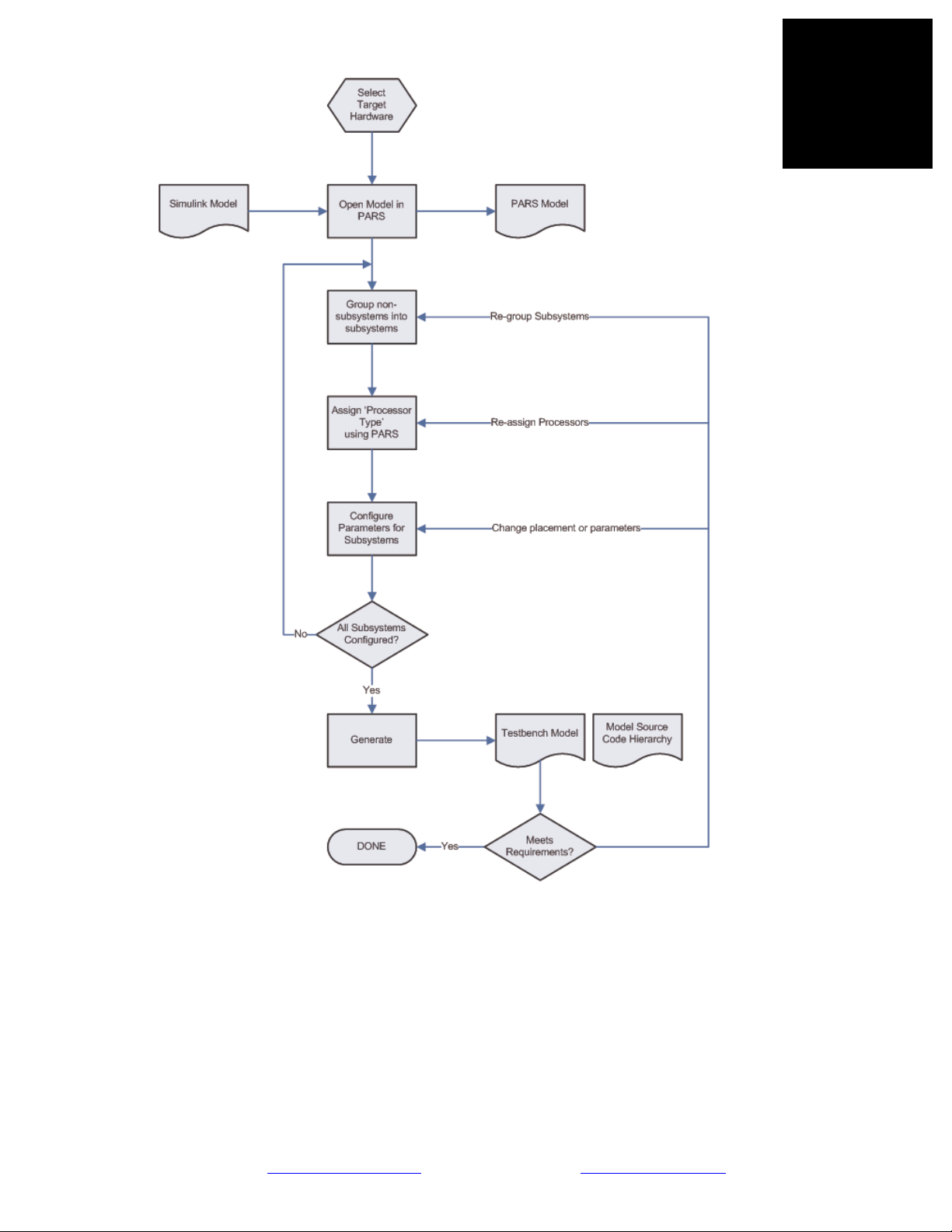
3.1.1. How PARS works with a model
PARS is a software system that automates many of the steps needed to actualize a Simulink model onto
embedded system hardware. In doing so, PARS invokes internal functions in Matlab, references
needed toolboxes, interprets and generates intermediate Simulink models and invokes external code
generation tools.
Figure 38 - PARS workflow and automation
The diagram above shows not only the process that PARS uses to generate a finished embedded
application, but also the points at which PARS provides automation.
Sundance Digital Signal Processing, Inc.
4790 Caughlin Parkway 233, Reno, NV 89519-0907, U.S.A.
email: sales@sundancedsp.com
Tel: +1 (775) 827-3103 www.sundancedsp.com
Page 35

Revision 11-wip-7
Page 35 of 70
Using PARS causes changes to the model in order to manage its metadata; these changes
are non-reversible, so PARS always works with a copy of the original model. The PARS
model is derived from the original model as follows:
Given a Simulink model: <model_name>.mdl, the PARS model will be:
<model_name>_PARS\<model_name>_PARS.mdl
For example, if your Simulink model is ‘C:\test\thing.mdl’, the PARS model will be
‘C:\test\thing_PARS\thing_PARS.mdl’
You only need to open the original Simulink model, PARS will create the working space for the PARS
model, perform the needed copy and preparation of the model. When you open a Simulink model,
PARS analyzes the corresponding PARS model and takes one of the following actions:
• If the PARS model does not exist, PARS creates it by taking a copy of the original model and
then silently opens the copy.
• If the PARS model exists and has a modification date later than that of the original model, the
PARS model will be opened silently.
• Otherwise, PARS will warn you that the models are inconsistent and offer to create a backup of
the PARS model; then it derives the working model by making a copy of the original model. No
changes will be made and nothing will be opened if you decline the offer.
Backups are made according to the following procedure:
1. A new sub-folder called ‘model_backup’ will be created if necessary.
2. The existing PARS model will be moved to this folder and renamed by adding a suffix of an
underscore and the PARS model's modification date and time.
Note that PARS does not attempt to detect/prevent you from modifying the .mdl files directly, but
please be aware that inconsistencies in state can be introduced so the practice is discouraged.
3.2. PREPARING FOR CODE GENERATION
Before attempting to generate any code with PARS, it is important to ensure that the target model will
be realizable in an embedded system. In order to do this, several configuration properties of the
simulation model should be set and the model verified in simulation.
Most notably, any system must be discrete. No continuous states are possible, as the underlying
computation fabric for the (known) embedded systems are based on synchronous logic operations.
Simulink provides a function to discretize a continuous model with the function ‘sldiscmdl’. An
example that uses this function is provided in the PARS demonstration applications.
Sundance Digital Signal Processing, Inc.
4790 Caughlin Parkway 233, Reno, NV 89519-0907, U.S.A.
email: sales@sundancedsp.com
Tel: +1 (775) 827-3103 www.sundancedsp.com
Page 36

Revision 11-wip-7
Page 36 of 70
3.2.1. Solver Configuration
When PARS generates code for the embedded model (for DSP targets), it uses ‘Fixed
Step, Discrete’ parameters. Therefore, it is recommended that the same settings be used
when simulating the model prior to code generation.
Figure 39 - Simulink model Solver parameters
It is also important to set the model’s stop time to ‘Inf’ before generating code. Some models will
generate different code for a non-infinite stop time; this is typically not what you want from an
autonomous embedded system.
It is also recommended to set the ‘Periodic Sample Time Constraint’ to ‘sample time independent’,
since that is precisely the kind of code that will be generated, but this is not always possible for all the
blocks that may exist in an arbitrary model.
Sundance Digital Signal Processing, Inc.
4790 Caughlin Parkway 233, Reno, NV 89519-0907, U.S.A.
email: sales@sundancedsp.com
Tel: +1 (775) 827-3103 www.sundancedsp.com
Page 37

Revision 11-wip-7
Page 37 of 70
3.2.2. Hardware Implementation
The hardware implementation parameters are straightforward. The embedded systems
that PARS can currently target are based on DSP from Texas Instruments.
Figure 40 - Simulink model Hardware Implementation parameters
Select ‘Texas Instruments’ and ‘C6000’ for device vendor and type. Select byte ordering according to
your vendor hardware instructions. Note that you can leave ‘Emulation Hardware’ set to ‘None”.
3.2.3. Summary
Group Parameter Value Notes
Solver ‘SolverType’ ‘Fixed-step’
Solver ‘Solver’ ‘FixedStepDiscrete’
Solver ‘StopTime’ ‘Inf’ Recommended prior to generation
Solver ‘SampleTimeConstraint’ ‘STIndependent’ Optional
Solver ‘SolverMode’ ‘SingleTasking’ Ignored if ‘SampleTimeConstraint’ =‘STIndependent’
Hardware ‘TargetHWDeviceType’ ‘Texas Instruments->C6000’
Table 2 - Model Parameters for Code Generation
Table 2, above, summarizes the options used by PARS when generating code. They are recommended
values to configure your PARS model so that simulation can best approximate the embedded
environment.
Sundance Digital Signal Processing, Inc.
4790 Caughlin Parkway 233, Reno, NV 89519-0907, U.S.A.
email: sales@sundancedsp.com
Tel: +1 (775) 827-3103 www.sundancedsp.com
Page 38

Revision 11-wip-7
Page 38 of 70
3.3. HARDWARE PROFILE SELECTION
Prior to opening a model in PARS, you need to select the target hardware profile that will
be used for the model development, allocation and generation. This enables PARS to
populate the fields for the DSP and FPGA task masks in order for you to be able to select
the processor name from the drop-down box in each of the masked subsystem.
You can do this from the PARS Control Panel via the ‘Tool’ Menu (Tool->PARS Options), or by
calling ‘PARSOptions’ in the Matlab command prompt.
Figure 41 - Selecting a hardware profile
In the PARSOptions panel, the ‘Hardware Profile’ is a drop-down box that lists the currently installed
hardware profiles you may choose from. Pick one and press ‘Accept’. This profile will remain in
effect until you change it again.
NOTE: When a PARS model is open, the ‘Tool’ menu option is grayed-out to discourage you from
changing options during an active development session. You should not change PARS options while
working with a model.
Please see Sec. 4.8. Hardware Description File, below, for additional details on adding your own
hardware profiles to your PARS installation.
Sundance Digital Signal Processing, Inc.
4790 Caughlin Parkway 233, Reno, NV 89519-0907, U.S.A.
email: sales@sundancedsp.com
Tel: +1 (775) 827-3103 www.sundancedsp.com
Page 39

Revision 11-wip-7
Page 39 of 70
3.4. PARTITIONING
One of the caveats of working with PARS is that all blocks within a model be contained
in subsystems prior to code generation. Each subsystem will become an atomic unit of
execution in the embedded system.
It is important to assign all top-level objects to a subsystem. PARS does not interpret non-subsystems
in the PARS model, not even documentation objects. Typically, the documentation objects would be
placed in the ‘HOST’ subsystem, and would therefore translate to the testbench.
The goal of partitioning a model is to group tasks that might schedule independently of other
operations. For DSP applications, this means tasks which may execute on different processors, or
which may execute at different times/rates on the same processor. For FPGA applications this means
logic that can execute concurrently. The more subsystem partitions your model has, the greater
opportunity for parallelism and concurrency. The trade-off, of course, is that connections between
subsystems take a finite amount of time. This is typically not covered by simulation, unless it is
modelled by a transmission delay block.
Strictly speaking, a model is partitioned into subsystems irrespective of the underlying hardware. The
subsystems group logically related operations together. In PARS, grouping subsystems does require
some consideration of the underlying hardware communication mechanisms primarily to deal with
limited connection resources and dataflow I/O performance.
When a model is partitioned, subsystems connect to other subsystems through input and output ports.
These connections define the exchange of (numeric) data between the logic/operations implemented in
the (atomic) subsystem.
3.4.1. Connections between subsystems
Connections between subsystems on the same processor are fast. On an FPGA they are implemented
by wires connecting the output and input stages together, often with a few cycles propagation delay.
On a DSP, they are implemented by operating-system defined libraries which currently involve a buffer
copy from the output buffer to the input buffer of the peer.
You can have an unlimited number of connections between subsystems on the same processor.
3.4.2. Connections between processors
Connections between subsystems on different processors are subject to the type of link interface that
exists between them. A hardware system topology describes processors and the ‘wires’ linking them.
Each ‘wire’ declares a link interface between the two processors in a point-to-point manner. See Figure
42, below.
Hardware manufacturers provide details on pin-mappings, software drivers and/or firmware IP to
implement their link interfaces. As long as you can connect the processors using supported devices,
PARS can create applications of any complexity and any intermixture of hardware types.
Sundance Digital Signal Processing, Inc.
4790 Caughlin Parkway 233, Reno, NV 89519-0907, U.S.A.
email: sales@sundancedsp.com
Tel: +1 (775) 827-3103 www.sundancedsp.com
Page 40

Revision 11-wip-7
Page 40 of 70
The hardware topology file names both the processor and the wires connecting them.
These names may be referenced in the model to ensure that the connections between the
subsystems are established over the desired wires7.
Figure 42 - Processors and wires in a hardware system8
In the diagram, processor P2 has one link, processors P1 and P5 have two links, P4 has three links and
P3 has 4 links. The number of declared links has bearing on the flexibility afforded to the architect
when assigning subsystems to processors.
PARS ensures that all the necessary software/firmware on every processor is included in the generated
application to implement the communications that are defined by the connections described. Although
there are currently two ‘types’ of processor: DSP and FPGA, they are treated the same with respect to
declarations of wires connecting them.
Between DSPs, a special type of link termed ‘virtual’ is possible. Connections between any DSP
subsystems can be established to any other DSP subsystem. This has the effect of minimizing the need
to consider the physical system when describing a model.
7
This suggests that a naming convention be followed to allow models to reference different topologies easily
8
Courtesy of 3L/Diamond v3.1.10 User Guide, pg. 27
Sundance Digital Signal Processing, Inc.
4790 Caughlin Parkway 233, Reno, NV 89519-0907, U.S.A.
email: sales@sundancedsp.com
Tel: +1 (775) 827-3103 www.sundancedsp.com
Page 41

Revision 11-wip-7
Page 41 of 70
Figure 43 - How routing is implemented between processors9
Figure 43, above, details three ways that subsystems communicate. Subsystem A and B communicate
via internal (fast) links on the same processor. Subsystem A and C communicate by using one of the
physical ‘wires’ between Processor X and Y. Subsystem B and D communicate using the ‘virtual
channel’ connection feature. PARS ensures that when the application is generated, the code necessary
to support this connection is loaded on to all the processors participating in establishing the connection;
in this case Processors X, Y and Z.
Unfortunately, this ‘virtual’ connection does not (currently) translate to the FPGA. Connections
between DSP and FPGA subsystems must be made with respect to the number and type of physical
links declared in the hardware system topology only. So for FPGA partitioning, the architect is advised
to group as much functionality onto the same FPGA as possible to minimize the number of connections
into and out of the FPGA-type processor.
9
Courtesy of 3L/Diamond v3.1.10 User Guide, pg. 33
Sundance Digital Signal Processing, Inc.
4790 Caughlin Parkway 233, Reno, NV 89519-0907, U.S.A.
email: sales@sundancedsp.com
Tel: +1 (775) 827-3103 www.sundancedsp.com
Page 42

Revision 11-wip-7
Page 42 of 70
For FPGA-to-FPGA connections, PARS includes an interface called ‘SCom’ which
allows for aggregating N:N connections over a single wire. This has the effect of
relaxing the restriction when making models that spread out onto multiple FPGA
subsystems. To use these, just use the SCom blocks provided in the ‘PARS Diamond
Blockset’. Please see sections “3.6.3. SCOM PB Tasks” and “4.4.6. SCOM Tasks”,
below for specific details.
3.4.3. Data Types for Connections
Another aspect of PARS that needs consideration when partitioning is the fact that PARS (currently)
can only interpret as relatively limited set of data types for connections.
Simulink Type Element size (bytes) Notes
‘double’ 8
‘single’ 4
‘int8’ 1 Must be vectorized into groups of 4, or complex groups of 2
‘uint8’ 1 Must be vectorized into groups of 4, or complex groups of 2
‘int16’ 2 Must be vectorized into groups of 2, or complex
‘uint16’ 2 Must be vectorized into groups of 2, or complex
‘int32’ 4
‘uint32’ 4
Table 3 - Allowable connection data types in PARS
Keep in mind that there is no restriction with data types used within a subsystem apart from those
imposed by RTW, RTW-EC (for DSP targets) and HDLCoder or Sysgen (for FPGA targets).
Figure 44 - Setting data types on Input/Output ports
Typically, one can set the output or input port data type to a specific type to ensure that the type is
appropriate for any given subsystem.
Sundance Digital Signal Processing, Inc.
4790 Caughlin Parkway 233, Reno, NV 89519-0907, U.S.A.
email: sales@sundancedsp.com
Tel: +1 (775) 827-3103 www.sundancedsp.com
Page 43

Revision 11-wip-7
Page 43 of 70
These restrictions are due to the fact that PARS needs to compute the total size of a data
communication that occurs at each simulation time step. So far, reliable computations
have only been possible when using the native C data types described in Table 3, above.
In order to transport arbitrary Simulink data types from subsystem to subsystem, it is
necessary to convert to a ‘standard’ elemental data type before the output port of a subsystem. On the
receiving subsystem, the signal is converted back to the ‘actual’ data type after the input port.
3.5. ALLOCATING PROCESSOR RESOURCES
Once a design is partitioned into subsystems, they may be assigned to processor types. This is
accomplished by selecting the subsystem and choosing ‘PARS->Create XXX Task’ from the dropdown menus of the PARS control panel. Alternatively, PARS provides friendly buttons to do this as
well.
Figure 45 - Shortcut buttons on PARS control panel
When a subsystem is assigned to a processor type, its outline changes color according to the processor
type it has been assigned. DSP is a shade of green, while FPGA is a shade of blue. This provides a
sual cue to understand the model partitioning at a glance.
vi
Figure 46 - General DSP task parameters panel
Once a processor type is assigned, double-clicking the subsystem now brings up a PARS-defined mask
that allows attributes assigned to the subsystem to be modified.
Sundance Digital Signal Processing, Inc.
4790 Caughlin Parkway 233, Reno, NV 89519-0907, U.S.A.
email: sales@sundancedsp.com
Tel: +1 (775) 827-3103 www.sundancedsp.com
Page 44

Revision 11-wip-7
Page 44 of 70
The specific controls available on this panel are described in detail in sections 4.2.2. and
4.3.2. below, for DSP and FPGA subsystems respectively. On the panel, the ‘Place task
on’ parameter gives a drop-down list box with each of the processors listed of the
allocated type.
For example, suppose a hardware topology contains two DSP processors and one FPGA. Then, each
DSP task would have the name of the DSP processors in the list, but not the FPGA processors. The
same for the FPGA task parameter panel, which would have only one FPGA choice listed.
If your active hardware topology does not have any of a particular kind of processor, then the menu
option and the button are disabled.
3.6. PRE-BUILT TASKS
3.6.1. DSP PB Tasks
3.6.2. FPGA PB Tasks
3.6.3. SCOM PB Tasks
3.7. HOST TESTBENCH STRATEGY
3.8. GENERATING APPLICATIONS
3.8.1. Pre-Compiled Libraries
3.8.2. FPGA Processors in Designs
When targeting FPGA processors in designs, it is important to avoid naming the subsystem with
keywords that are used in the VHDL language. For example, one should not use a subsystem name
‘Generate’, as that will create conflict with the VHDL parser.
Sundance Digital Signal Processing, Inc.
4790 Caughlin Parkway 233, Reno, NV 89519-0907, U.S.A.
email: sales@sundancedsp.com
Tel: +1 (775) 827-3103 www.sundancedsp.com
Page 45

3.9. RUNNING THE TEST BENCH
3.10. RESTRICTIONS
3.11. COMMON ISSUES
3.11.1. Loop Deadlock
Detecting
Solution
3.11.2. Out-of-order Deadlock
Detecting
Solution
3.11.3. Rate Deadlock
Revision 11-wip-7
Page 45 of 70
Detecting
Solution
Sundance Digital Signal Processing, Inc.
4790 Caughlin Parkway 233, Reno, NV 89519-0907, U.S.A.
email: sales@sundancedsp.com
Tel: +1 (775) 827-3103 www.sundancedsp.com
Page 46

Revision 11-wip-7
Page 46 of 70
4. PARS COMPONENT REFERENCE
4.1. PARS CONTROL PANEL
4.1.1. Overview
4.1.2. File Menu
4.1.3. PARS Menu
Create DSP Task
Create FPGA Task
Create HOST Task
Generate Application
4.1.4. Tool Menu
PARSOptions
Hardware Profile Selection
FPGA Task Creation Selection
Target Type Selection
Code Generation Type Selection
PARS Local Path Field
Model Properties Switch
Verify Optimization Switch
Check Model
4.1.5. Help Menu
User Guide
About
4.2. DSP TASKS
4.2.1. Overview
4.2.2. Mask Options
email: sales@sundancedsp.com
Sundance Digital Signal Processing, Inc.
4790 Caughlin Parkway 233, Reno, NV 89519-0907, U.S.A.
Tel: +1 (775) 827-3103 www.sundancedsp.com
Page 47

Task Placement Selection
Target Processor Selection
Task Memory Size Field
Task Parameters Field
4.2.3. GRT vs. ERT
Examples
4.3. FPGA TASKS
4.3.1. Overview
4.3.2. Mask Options
Task Placement Selection
Revision 11-wip-7
Page 47 of 70
Clock Source Field
4.3.3. Clock Domain Considerations
4.3.4. HDLCoder vs. Xilinx System Generator
Examples
4.4. PARS DIAMOND LIBRARY
4.4.1. Overview
4.4.2. Diamond Blockset
Diamond Configuration Block
DSPLink Block
memblock Block
Bind Input Block
Bind Output Block
Task Input Block
Task Output Block
4.4.3. Device Driver Tasks
Sundance Digital Signal Processing, Inc.
4790 Caughlin Parkway 233, Reno, NV 89519-0907, U.S.A.
email: sales@sundancedsp.com
Tel: +1 (775) 827-3103 www.sundancedsp.com
Page 48

Connect From Block
Connect To Block
4.4.4. DSP Tasks
ab105_bridge
ddr2_cmd_to_5x32
DelayBlock
reframe
SMT317
Config317
Data317
Revision 11-wip-7
Page 48 of 70
SMT319
Config319
Config319_ParsCallBack.m
SMT350
ControlCdm7005
Config350
SMT364
Config364
Config364_ParsCallBack.m
SMT377
Config377
4.4.5. FPGA Tasks
fifo4K_32
strorage
SMT350
Sundance Digital Signal Processing, Inc.
4790 Caughlin Parkway 233, Reno, NV 89519-0907, U.S.A.
email: sales@sundancedsp.com
Tel: +1 (775) 827-3103 www.sundancedsp.com
Page 49

SMT350_ADC
SMT350_ADCCM
SMT350_CDM7005
SMT350_DAC
SMT350_DacClk1_CM
SMT350_DDS
SMT351T
smt351t_pb_1G_ddr2_a
smt351t_pb_1G_ddr2_b
SMT377
Revision 11-wip-7
Page 49 of 70
SMT377_DAC
4.4.6. SCOM Tasks
SCOM_Rx1
SCOM_Rx2
SCOM_Rx6
SCOM_Tx1
SCOM_Tx2
SCOM_Tx6
4.5. DSP PRE-BUILT TASKS
4.5.1. Overview
4.5.2. Usage
4.5.3. Template of a DSP PB Task
4.5.4. CPBT Operation for DSP Tasks
4.5.5. Bind Input Block
4.5.6. Bind Output Block
Sundance Digital Signal Processing, Inc.
4790 Caughlin Parkway 233, Reno, NV 89519-0907, U.S.A.
email: sales@sundancedsp.com
Tel: +1 (775) 827-3103 www.sundancedsp.com
Page 50

Revision 11-wip-7
Page 50 of 70
4.5.7. Examples
4.6. FPGA PRE-BUILT TASKS
4.6.1. Overview
4.6.2. Usage
4.6.3. Template of an FPGA PB Task
4.6.4. CPBT Operation for FPGA Tasks
4.6.5. Examples
4.7. SCOM WRAPPER TASKS
4.7.1. Overview
4.7.2. Usage
4.7.3. Hierarchy of SCOM Task Wrappers
Folder Organization
4.7.4. SCOM Task Table
4.7.5. Deriving New Variants
SCOM Block
SCOM BSP
4.7.6. Examples
4.8. HARDWARE DESCRIPTION FILE
4.8.1. Overview
4.8.2. Sections (.m file based input)
Descriptive Header
Processor Declarations
Name
PROCTYPE
Command
Sundance Digital Signal Processing, Inc.
4790 Caughlin Parkway 233, Reno, NV 89519-0907, U.S.A.
email: sales@sundancedsp.com
Tel: +1 (775) 827-3103 www.sundancedsp.com
Page 51

Type
ClockFreq
DSP Type Fields
Optimization Type
FPGA Type Fields
FPGAType
Wire Declarations
Name
StartProcessorName
StartProcessorPort
Revision 11-wip-7
Page 51 of 70
EndProcessorName
EndProcessorPort
Command
Footer
4.8.3. Model Based Input (.mdl file)
Sundance Digital Signal Processing, Inc.
4790 Caughlin Parkway 233, Reno, NV 89519-0907, U.S.A.
email: sales@sundancedsp.com
Tel: +1 (775) 827-3103 www.sundancedsp.com
Page 52

5. PARS GENERATED CODE
5.1. PARS HIERARCHY
5.2. DSP TASKS
5.2.1. Structure
5.2.2. Files (Production)
_task_main.c
_task_main.h
_task.c
_task.h
makefile
Revision 11-wip-7
Page 52 of 70
5.2.3. Variants
Profiling
Debugging
5.3. FPGA TASKS
5.3.1. Structure
5.3.2. Common Files
ab105(_pkg).vhd
pars_memblk_cmdcore.vhd
pars_memblk_pkg.vhd
pars_memblk_resolve.vhd
pars_memblk_taskstate.vhd
pars_profile(_pkg).vhd
task_interface_pkg.vhd
5.3.3. Scalar vs. Vector Inputs
5.3.4. Files
Sundance Digital Signal Processing, Inc.
4790 Caughlin Parkway 233, Reno, NV 89519-0907, U.S.A.
email: sales@sundancedsp.com
Tel: +1 (775) 827-3103 www.sundancedsp.com
Page 53

_task.fcd
_task(_pkg).vhd
5.4. PRE-BUILT TASKS
5.4.1. Overview
5.4.2. Files
ab105_bridge.tsk
ab105_proxy.tsk
chan2mux.tsk
link2link.tsk
log2chan.tsk
Revision 11-wip-7
Page 53 of 70
Multiplex.tsk
mux2chan.tsk
silo2switch.tsk
5.5. PARS CONFIGURATION FILE
5.5.1. Overview
5.5.2. Diamond Configuration Block
5.5.3. Sections
PROCTYPE Declarations (Diamond Config)
Processor Declarations (Hardware Description)
Wire Declarations (Hardware Description)
Tasks (Model)
Control/Status Daisy Chain (Model)
Bindings (Model)
HOST Multiplexer (Model)
Footer (Diamond Config)
4790 Caughlin Parkway 233, Reno, NV 89519-0907, U.S.A.
email: sales@sundancedsp.com
Sundance Digital Signal Processing, Inc.
Tel: +1 (775) 827-3103 www.sundancedsp.com
Page 54

5.6. PARS APPLICATION
5.6.1. General Behavior
5.6.2. Boot Progression
Revision 11-wip-7
Page 54 of 70
Sundance Digital Signal Processing, Inc.
4790 Caughlin Parkway 233, Reno, NV 89519-0907, U.S.A.
email: sales@sundancedsp.com
Tel: +1 (775) 827-3103 www.sundancedsp.com
Page 55

6. HARDWARE
6.1. PARS TARGET HARDWARE
6.1.1. Types
6.1.2. Pre-Condition Requirements
6.1.3. Sundance Hardware
Modules
Carriers
Link-Layer Drivers
6.1.4. VMetro Hardware
PMC-FPGA03F
Revision 11-wip-7
Page 55 of 70
6.1.5. 3rd Party Board Support
Bootloader Requirement
Template
Link-Layer Driver Model
Template
template_hal.h
template_hal.cpp
makefile
Sundance Digital Signal Processing, Inc.
4790 Caughlin Parkway 233, Reno, NV 89519-0907, U.S.A.
email: sales@sundancedsp.com
Tel: +1 (775) 827-3103 www.sundancedsp.com
Page 56

Revision 11-wip-7
Page 56 of 70
7. ADVANCED FEATURES
7.1. TASK CONTROL/STATUS INTERFACE
7.1.1. Overview
7.1.2. AB105 Protocol Module
7.1.3. Task IDs
7.1.4. Taskstate Protocol
7.1.5. Operation under HIL
7.1.6. Operation in Standalone (embedded) Systems
7.2. PROFILING INTERFACE
7.2.1. Overview
7.2.2. PARS-Profile Module
7.2.3. Profile Report
7.2.4. Operation under HIL
7.2.5. Operation in Standalone (embedded) Systems
7.3. DEBUGGING (LOG) INTERFACE
7.3.1. Overview
7.3.2. Logging System Pre-Built Tasks
log2chan.tsk
silo2switch.tsk
link2link.tsk
7.3.3. Tracking Task Dataflow
7.3.4. DSP PB Tasks
7.3.5. Log Report Format
7.4. DEBUGGING (JTAG EMULATORS)
7.4.1. Overview
Sundance Digital Signal Processing, Inc.
4790 Caughlin Parkway 233, Reno, NV 89519-0907, U.S.A.
email: sales@sundancedsp.com
Tel: +1 (775) 827-3103 www.sundancedsp.com
Page 57

Revision 11-wip-7
Page 57 of 70
7.4.2. app2coff
7.4.3. TI CCS Operation
7.5. REBUILDING OUTSIDE OF PARS
7.5.1. Application Build Script
7.5.2. Changing Debugging Level
Sundance Digital Signal Processing, Inc.
4790 Caughlin Parkway 233, Reno, NV 89519-0907, U.S.A.
email: sales@sundancedsp.com
Tel: +1 (775) 827-3103 www.sundancedsp.com
Page 58

8. DEMOS AND EXAMPLES
8.1. ADDONE INTEGER
8.1.1. Description
8.1.2. DSP Target
8.1.3. FPGA Target
Sysgen
HDLCoder
8.1.4. Profiling Output
8.2. FILTER BANK
8.2.1. Description
Revision 11-wip-7
Page 58 of 70
The filter bank demo consists of three filters working in parallel to manipulate the frequency response
of a signal in real time. The model contains several blocks and subsystems to make a good
demonstration on partitioning and processor selection.
Sundance Digital Signal Processing, Inc.
4790 Caughlin Parkway 233, Reno, NV 89519-0907, U.S.A.
email: sales@sundancedsp.com
Tel: +1 (775) 827-3103 www.sundancedsp.com
Page 59

Revision 11-wip-7
Page 59 of 70
Figure 47 - Filter Bank original model
In this model, a file containing audio data is read continuously, distributed to three selectable gain
blocks, filtered, summed and re-rendered onto audio hardware. To add some interactivity in the
demonstration, the gain blocks can be manipulated in real time during test bench simulation.
Sundance Digital Signal Processing, Inc.
4790 Caughlin Parkway 233, Reno, NV 89519-0907, U.S.A.
email: sales@sundancedsp.com
Tel: +1 (775) 827-3103 www.sundancedsp.com
Page 60

Revision 11-wip-7
8.2.2. DSP Target
One Task
Five Task
Eight Task
8.2.3. FPGA Target
Sysgen
HDLCoder
8.2.4. Profiling Output
8.3. LEAST MEAN SQUARE ERROR
8.3.1. Description
Page 60 of 70
8.3.2. DSP Target
One DSP
Two DSP
8.3.3. FPGA Target
Sysgen
HDLCoder
8.3.4. Profiling Output
8.4. ACOUSTIC NOISE CANCELLATION
8.4.1. Description
8.4.2. DSP Target
One DSP
Two DSP
8.4.3. FPGA Target (?)
8.4.4. Profile Output
8.5. FEEDBACK CONTROL SYSTEM (GM)
Sundance Digital Signal Processing, Inc.
4790 Caughlin Parkway 233, Reno, NV 89519-0907, U.S.A.
email: sales@sundancedsp.com
Tel: +1 (775) 827-3103 www.sundancedsp.com
Page 61

8.5.1. Description
8.5.2. DSP Target
8.5.3. FPGA Target
8.5.4. Profiling Output
8.6. AEROSPACE GUIDANCE
8.6.1. Description
Required Toolboxes
8.6.2. DSP Target
8.6.3. Profiling Output
Revision 11-wip-7
Page 61 of 70
Sundance Digital Signal Processing, Inc.
4790 Caughlin Parkway 233, Reno, NV 89519-0907, U.S.A.
email: sales@sundancedsp.com
Tel: +1 (775) 827-3103 www.sundancedsp.com
Page 62

Revision 11-wip-7
Page 62 of 70
9. INSTALLATION
9.1. RESTRICTIONS
9.2. INSTALLED HIERARCHY
9.3. STEP-BY-STEP WALKTHRU
9.4. VERIFYING THE INSTALLATION
The PARS installation can be verified by using the ver command in the Matlab console. It is important
to ensure that the version numbers are consistent.
>> ver
------------------------------------------------------------------------------------MATLAB Version 7.5.0.342 (R2007b)
MATLAB License Number: xxxxxxx
Operating System: Microsoft Windows XP Version 5.1 (Build 2600: Service Pack 3)
Java VM Version: Java 1.6.0 with Sun Microsystems Inc. Java HotSpot(TM) Client VM mixed mode
------------------------------------------------------------------------------------MATLAB Version 7.5 (R2007b)
Simulink Version 7.0.1 (R2007b+) <<
F
ixed-Point Toolbox Version 2.1.1 (R2007b+) <<
PARS Version 11.0.0 (R2007b+)
PARS AddOns Version 11.0.0 (R2007b+)
PARS Diamond (TI DSP C6000) Version 11.0.0 (R2007b+)
PARS Diamond ERT target (TI DSP C6000) Version 11.0.0 (R2007b+)
PARS Diamond FPGA (HDL Coder) Version 11.0.0 (R2007b+)
PARS Diamond FPGA (Xilinx Sysgen) Version 11.0.0 (R2007b+)
PARS Diamond GRT target (TI DSP C6000) Version 11.0.0 (R2007b+)
Real-Time Workshop Version 7.0.1 (R2007b+) <<
Real-Time Workshop Embedded Coder Version 5.0.1 (R2007b+) <<
ignal Processing Blockset Version 6.6 (R2007b)
S
Signal Processing Toolbox Version 6.8 (R2007b)
Simulink Fixed Point Version 5.5.1 (R2007b+)
Xilinx System Generator Version 10.1.3 build 1386
Figure 48 - PARS versions as seen by Matlab
If these version numbers are inconsistent, please contact your reseller or license administrator.
<<< the table above must be updated once PARS 11 is released >>>
Sundance Digital Signal Processing, Inc.
4790 Caughlin Parkway 233, Reno, NV 89519-0907, U.S.A.
email: sales@sundancedsp.com
Tel: +1 (775) 827-3103 www.sundancedsp.com
Page 63

Revision 11-wip-7
Page 63 of 70
10. ADDONS
10.1. OVERVIEW
10.2. SMT6045 (UNIVERSAL TARGET SERVICES)
10.2.1. Overview
10.2.2. Features
10.2.3. Installed Hierarchy
10.2.4. Pre-Built Task Descriptions
<<<each task has description page>>>
10.2.5. DSP Interface Descriptions
<<<each function callable by DSP has description page>>>
10.2.6. HOST Interface Descriptions
<<<each function callable by HOST code has description page>>>
10.2.7. FPGA Modules Descriptions
General Concepts
Parametric Diamond Wrappers
<<<each wrapper has description page>>>
10.3. MODULES
10.3.1. Overview
10.3.2. Features
10.3.3. Installed Hierarchy
10.3.4. Pre-Built Task Descriptions
<<<each task has description page>>>
10.3.5. DSP Interface Descriptions
<<<each function callable by DSP has description page>>>
10.3.6. HOST Interface Descriptions
Sundance Digital Signal Processing, Inc.
4790 Caughlin Parkway 233, Reno, NV 89519-0907, U.S.A.
email: sales@sundancedsp.com
Tel: +1 (775) 827-3103 www.sundancedsp.com
Page 64

Revision 11-wip-7
Page 64 of 70
<<<each function callable by HOST code has description page>>>
10.3.7. FPGA Modules Descriptions
General Concepts
<<<each wrapper has description page>>>
10.4. SCOM (SUNDANCE COMMUNICATION INTERFACE)
10.4.1. Overview
10.4.2. Features
10.4.3. Installed Hierarchy
10.4.4. Nomenclature
10.4.5. Pre-Defined Wrapper Interface
1-port
2-port
6-port
10.4.6. Derivation of N-port Wrappers
Sundance Digital Signal Processing, Inc.
4790 Caughlin Parkway 233, Reno, NV 89519-0907, U.S.A.
email: sales@sundancedsp.com
Tel: +1 (775) 827-3103 www.sundancedsp.com
Page 65

Revision 11-wip-7
Page 65 of 70
11. KNOWLEDGE BASE
11.1. DESCRIPTION
11.2. ENTRIES
<<<to be organized into categories after all items are written>>>
Sundance Digital Signal Processing, Inc.
4790 Caughlin Parkway 233, Reno, NV 89519-0907, U.S.A.
email: sales@sundancedsp.com
Tel: +1 (775) 827-3103 www.sundancedsp.com
Page 66

12. REFERENCES AND LINKS
Revision 11-wip-7
Page 66 of 70
Sundance Digital Signal Processing, Inc.
4790 Caughlin Parkway 233, Reno, NV 89519-0907, U.S.A.
email: sales@sundancedsp.com
Tel: +1 (775) 827-3103 www.sundancedsp.com
Page 67

Revision 11-wip-7
Page 67 of 70
13. LICENSING AND INTELLECTUAL PROPERTY RIGHTS
END-USER LICENSE AGREEMENT for
PARS
Parallel Application
Rapid Simulation
S
undance Digital Signal Processing Inc.
Referred to hereafter as (SDSP)
: This END-USER LICENSE AGREEMENT
(Or "AGREEMENT") is a Legal Agreement between you (either an individual or entity) and SDSP.
The "LICENSED MATERIALS" subject to this Agreement include the enclosed software programs and
documentation and any "on-line" or electronic documentation associated with the software programs. The
"LICENSED MATERIALS" (collectively referred to as the "SOFTWARE") may include certain SDSP
proprietary software programs that. By installing, copying or otherwise using the "LICENSED
MATERIALS", you agree to abide by the following provisions.
You assume responsibility for the selection of the SOFTWARE to achieve your intended results, and for
the installation, use and results obtained from the SOFTWARE.
1. SOFTWARE LICENSE - The Licensed Materials are protected by copyright laws, internationa
copyright treaties, and trade secret laws, as well as other intellectual property laws and treaties. The
Licensed Materials are licensed, not sold to you, and can only be used in accordance with the terms of
this Agreement. SDSP retains title and ownership of the Licensed Materials, including all intellectual
property rights.
l
a) Restrictions - This license is for a single-user host computer. You may not install the Licensed
Materials on a network server or otherwise use the Licensed Materials on more than one host
computer at the same time. Additionally, if this package contains multiple versions of the Licensed
Materials, you may only use one version of the Licensed Materials on a single host computer. You
may either make one copy of the Licensed Materials for archival purposes or copy the Licensed
Sundance Digital Signal Processing, Inc.
4790 Caughlin Parkway 233, Reno, NV 89519-0907, U.S.A.
email: sales@sundancedsp.com
Tel: +1 (775) 827-3103 www.sundancedsp.com
Page 68

Revision 11-wip-7
Page 68 of 70
Materials to another medium and keep the original Licensed Materials for archival
purposes. Other than as expressly set forth in Section 1(b) below, you may not
otherwise copy or reproduce the Licensed Materials. In no event may you use two
copies or versions of the Licensed Materials on more than one host computer at the
same time.
b) Copy, modify, and merge - You may copy the SOFTWARE into any machine-readable or printed
f
orm for backup purposes in support of your use of the SOFTWARE on the single-user machine.
You may not modify the SOFTWARE. You may merge it into another program for your use on the
single-user machine. Any portion of this SOFTWARE merged into another program will continue
to be subject to the terms and conditions of this Agreement. You must reproduce and include the
copyright notice (s) on any copy, modification, or portion merged into another program. The
license entitles the user to 20 runtime licenses. To obtain additional runtime licenses please contact
SDSP.
c) Termination - This license is effective until terminated. Without prejudice to any other rig
hts,
SDSP may terminate your right to use the Licensed Materials and any applications generated using
the Licensed Materials under this Agreement if you fail to comply with the terms of this
Agreement. In such event, you must destroy all copies of the SOFTWARE and all of its
component parts.
2. INTELLECTUAL PROPERTY RIGHTS. The Licensed Materials contain copyrighted material, trade
secrets and other proprietary information. In order to protect the Licensed Materials, and except as
specifically permitted by statute, you may not decompile, reverse engineer, disassemble or otherwise
translate the object code versions of the software programs included in the Licensed Materials to
human-perceivable form. If you are a corporation you agree you will use your best efforts to prevent
your employees and contractors from decompiling, reverse engineering, disassembling, modifying or
translating the Licensed Materials. In no event may you alter, remove or destroy any copyright notice
included in the Licensed Materials. SDSP reserves all rights not specifically granted under this
Agreement.
3. APPLICABILITY. This license only applies to the version of the SOFTWARE for which it was
ssued. It does not automatically entitle the licensee to software advancements and functionality to be
i
offered in future versions of the software. The licensee can obtain future versions of the SOFTWARE
by prior agreement with SDSP.
4. LIMITATIONS. SDSP MAKES NO WARRANTY OF ANY KIND, EITHER EXPRESSED OR
IMPLIED, INCLUDING, BUT NOT LIMITED TO, THE IMPLIED WARRANTIES OF
MERCHANTABILITY AND FITNESS FOR A PARTICULAR PURPOSE. THE ENTIRE RISK AS
TO THE QUALITY AND PERFORMANCE OF THE SOFTWARE IS WITH YOU. SHOULD THE
SOFTWARE PROVE DEFECTIVE, YOU (NOT SDSP) ASSUME THE ENTIRE COST OF ALL
NECESSARY SERVICING, REPAIR, OR CORRECTION.
Sundance Digital Signal Processing, Inc.
4790 Caughlin Parkway 233, Reno, NV 89519-0907, U.S.A.
email: sales@sundancedsp.com
Tel: +1 (775) 827-3103 www.sundancedsp.com
Page 69

Revision 11-wip-7
Page 69 of 70
5. I
N NO EVENT WILL SDSP BE LIABLE TO YOU FOR ANY DAMAGES,
INCLUDING ANY LOST PROFITS, LOSS OF BUSINESS INFORMATION,
BUSINESS INTERRUPTION, LOST SAVINGS OR OTHER INCIDENTAL OR
CONSEQUENTIAL DAMAGES ARISING OUT OF THE USE OR INABILITY TO USE SUCH
SOFTWARE, EVEN IF SDSP HAS BEEN ADVISED OF THE POSSIBILITY OF SUCH
DAMAGES, OR FOR ANY CLAIM BY ANY OTHER PARTY.
OU ACKNOWLEDGE THAT YOU HAVE READ THIS AGREEMENT, UNDERSTAND IT,
6. Y
AND AGREE TO BE BOUND BY ITS TERMS AND CONDITIONS. YOU FURTHER AGREE
THAT IT IS THE COMPLETE AND EXCLUSIVE STATEMENT OF THE AGREEMENT
BETWEEN YOU AND SDSP WHICH SUPERSEDES ANY PROPOSAL OR PRIOR
AGREEMENT, ORAL OR WRITTEN, AND ANY OTHER COMMUNICATIONS BETWEEN US
RELATING TO THE SUBJECT MATTER OF THIS AGREEMENT.
7. EXPORT CONTROL. The re-export of United States origin software and documentation is subject to
the Export Administration Act of 1969 as amended. Compliance with such regulations is your
responsibility.
8. U.S. GOVERNMENT RESTRICTED RIGHTS. This computer software and documentation are
provided with RESTRICTED RIGHTS. Use, duplication, or disclosure by the Government is subject
to restrictions as set forth in subparagraph (c)(1)(ii) of the Rights in Technical Data and Computer
Software clause at DFARS 252.227-7013 (Oct. 1988) or if provided under a contract or subcontract
with NASA or a civilian agency of the Government, to the restrictions set forth is such contract or
subcontract.
9. Should you have any questions concerning this Agreement, or if you desire to contact SDSP for any
reason, please contact SDSP.
Copyright (C) 1999-2009, Sundance Digital Signal Processing Inc.
Sundance Digital Signal Processing, Inc.
4790 Caughlin Parkway 233, Reno, NV 89519-0907, U.S.A.
email: sales@sundancedsp.com
Tel: +1 (775) 827-3103 www.sundancedsp.com
Page 70

14. INDEX
Revision 11-wip-7
Page 70 of 70
Sundance Digital Signal Processing, Inc.
4790 Caughlin Parkway 233, Reno, NV 89519-0907, U.S.A.
email: sales@sundancedsp.com
Tel: +1 (775) 827-3103 www.sundancedsp.com
 Loading...