

Page 1

FC203B - Power Spectrum
Interleaver
FPGA Module
User’s Guide
Copyright © Sundance Digital Signal Pro cessing Inc.
All rights reserved. No part of this document may be reproduced, translated,
stored in a retrieval system, or transmitted, in any form or by any means,
electronic, mechanical, photocopying, recording or otherwise, without prior
written permission of the owner.
If this copy is no longer in use, return to sender.
Note:
Page 2
Page 2 of 2
Revision 0.5
AUTHORS
Name Signature Date
F. Huettig 6-Apr-07
DOCUMENT HISTORY
Date Initials Revision Description of Change
19-Feb-07 FH 0.0 Initial Release for Internal Review
2-Apr-07 FH 0.1 Changed definition of SPAN, removed FDMA_IN
port and need for FC203C.
5-Apr-07 FH 0.2 Fixed table 3, added C>1 requirement
6-Apr-07 FH 0.3 Added “Known Issues”
8-Apr-07 FH 0.5 Added resource utilization
Sundance Digital Signal Processing Inc.
4790 Caughlin Parkway 233, Reno, NV 89519-0907, U.S.A.
Tel: +1 (775) 827-3103, Fax: +1 (775) 827-3664, email: sales@sundancedsp.com
www.sundancedsp.com
Page 3

Page 3 of 3
Revision 0.5
Table of Contents
1. GENERAL DESCRIPTION...................................................................................................4
2. I/O DESCRIPTION.................................................................................................................5
3. KNOWN ISSUES...................................................................................................................8
4. PRESENTATION...................................................................................................................8
5. USAGE....................................................................................................................................9
6. VERIFICATION...................................................................................................................11
7. DELIVERABLES.................................................................................................................12
8. LICENSING AND PROPERTY RIGHTS...........................................................................12
9. ORDERING INFORMATION.............................................................................................12
Table of Figures
Figure 1 – FC203B Component Diagram.......................................................................................4
Sundance Digital Signal Processing Inc.
4790 Caughlin Parkway 233, Reno, NV 89519-0907, U.S.A.
Tel: +1 (775) 827-3103, Fax: +1 (775) 827-3664, email: sales@sundancedsp.com
www.sundancedsp.com
Page 4
Page 4 of 4
Revision 0.5
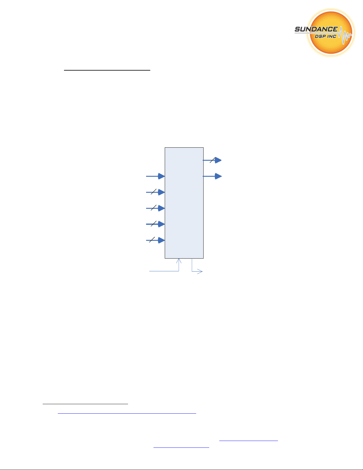
1. GENERAL DESCRIPTION
This sub-component implements the time slot assembly of the FC203 component group. The
FC203A provides raw spectral information from groups of channels; the FC203B component
exists to merge the data from multiple channels into one time-multiplexed spectral information
stream.
In order for it to be used within a Diamond/FPGA system, the I/O interfaces are ‘standardized’ to
the model described by Diamond1.
FC203B
FDMA_OUT
32
FDMA_CM_IN
F0_IN
64
F1_IN
64
F2_IN
64
F3_IN
64
FDMA_CM_OUT
CTRL_IN
Figure 1 – FC203B Component Diagram
1
See: http://www.3l.com/Diamond/Documentation/Diamond.pdf (Chapter 28, “FPGA Tasks”)
STATUS_OUT
Sundance Digital Signal Processing Inc.
4790 Caughlin Parkway 233, Reno, NV 89519-0907, U.S.A.
Tel: +1 (775) 827-3103, Fax: +1 (775) 827-3664, email: sales@sundancedsp.com
www.sundancedsp.com
Page 5

Page 5 of 5
Revision 0.5
2. I/O DESCRIPTION
The FC203B component presents as a pure-FPGA ‘task’, and implements the following
interface:
Port Name Channel Valid
Direction Description
Width
FMDA_CM_IN 0 20 Input Encodes the number of frequency bins and
channels implemented in FDMA_IN
F0_IN..F3_IN 1..4 64 Input In-Phase/Quadrature components,
frequency domain data, two channels per
link
CTRL_IN 5 32 Input Control Word
FDMA_OUT 0 32 Output Frequency domain multiple access
(highway output)
FDMA_CM_OUT 1 20 Output Encodes the number of frequency bins and
channels implemented in FDMA_OUT
STATUS_OUT 2 32 Output Pass-through control/status
Table 1 –FC203B Interfaces
Additional port descriptions are provided below:
FDMA_CM_IN
This port drives the current configuration of the FDMA_OUT port, as described below. Bits
0...12 represent the number of frequency bins, M (up to 4096) while bits 16...19 represent the
number of channels that are interleaved, C. A ‘C’ value of zero will create 16 channels in the
FDMA_highway, although this module is only capable of filling up to 8. This port is suitable for
connecting to any FDMA_CM_OUT port.
Signal Bits Mode Description
M 12..lsb R/W Number of samples per frame
RESERVED 15..13 R/W Pass-through (reserved)
C 19..16 R/W Number of active channels
RESERVED 31..20 R/W Pass-through (reserved)
Table 2 – Format of FDMA_CM_IN control word
NOTE: To simplify the FPGA logic, the control word is assumed to be static while the module is
enabled. Changes to M or C while any ENABLE bit is set will result in unpredictable output.
NOTE: C=1 is currently not supported.
Sundance Digital Signal Processing Inc.
4790 Caughlin Parkway 233, Reno, NV 89519-0907, U.S.A.
Tel: +1 (775) 827-3103, Fax: +1 (775) 827-3664, email: sales@sundancedsp.com
www.sundancedsp.com
Page 6

Page 6 of 6
Revision 0.5
F0_IN .. F3_IN
These are dual-channel partitioned frequency data ports. Data values are groups of 64-bit values
in bursts of SPAN qwords. The 64-bit values consist of the in-phase and quadrature components
(16-bit two’s complement as described in the FC108 User Manual) of two channels. This port is
suitable for connecting to the Fx_OUT ports of the FC203A subcomponent.
Bit 15..0 I0(0) I0(1) … I0(SPAN – 1)
Bit 31..16 Q0(0) Q0(1) … Q0(SPAN – 1)
Bit 47..32 I1(0) I1(1) … I1(SPAN – 1)
Bit 63..48 Q1(0) Q1(1) … Q1(SPAN – 1)
Table 3 – Stream Format of Fx_IN Port, low-frequency channel, LOW_FREQ = 0
NOTE: The FC203B module has 1024 samples worth of internal buffering on each of the 4
inputs (a sample includes one in-phase and one quadrature value). The system design must
insure that this is sufficient to handle the worst-case combination of lag between any pair of
channels, PLUS the worst-case latency of the FDMA_OUT output sink. A FIFO at the
FDMA_OUT port may help with output latency, but FIFOs will not help between the FC203A
and FC203B because the inputs to FC203B are “always ready.”
CTRL_IN
Control miscellaneous parameters and features of the FC203B subcomponent. The port accepts
data one 32-bit word at a time. The bit definitions are compatible with the definition used in the
FC203A module.
Signal Bits Mode Description
RESERVED 15..lsb R/W Pass-through (reserved)
SPAN 25..16 R/W Select number of active frequency bins
RESERVED 27..26 R/W Pass-through (reserved)
ENABLE msb..28 R/W Channel-pair enable
Table 4 - FC203B Control Word
The FC203B module ignores some of the bits; they exist to enable the configuration of multiple
modules (including FC203A) in a daisy-chain fashion. SPAN determines the number of
frequency bins that are present in the inbound Fx_IN streams. SPAN must be less than or equal
to M (from FDMA_CM_IN). ENABLE determines how many of the Fx_IN streams are to be
packaged on the FDMA_OUT sequence. Each bit in the ENABLE control word allows the
corresponding Fx_IN stream to be inserted into the output. Enables occur according to the
following pattern:
Sundance Digital Signal Processing Inc.
4790 Caughlin Parkway 233, Reno, NV 89519-0907, U.S.A.
Tel: +1 (775) 827-3103, Fax: +1 (775) 827-3664, email: sales@sundancedsp.com
www.sundancedsp.com
Page 7

Page 7 of 7
Revision 0.5
Enable = xxx1b F0_IN inserted at channels 0 & 1
Enable = xx1xb F1_IN inserted at channel s 2 & 3
Enable = x1xxb F2_IN inserted at channel s 4 & 5
Enable = 1xxxb F3_IN inserted at channels 6 & 7
Table 5 – Enable Configuration
For channels which are not enabled (corresponding bit is clear) and which are within the current
value of C from FDMA_CM_IN, the data placed on FDMA_OUT will be set to zero.
NOTE: To simplify the FPGA logic, the control word is assumed to be static while the module is
enabled. Changes to SPAN while any ENABLE bit is set will result in unpredictable output.
FDMA_OUT
This is a multi-channel frequency domain highway. Data values are groups of C 32-bit values
inside M micro-frames. The 32-bit values consist of the in-phase and quadrature components
(16-bit twos-complement as described in the FC108 User Manual) of one channel packed into a
32-bit word. The micro-frame represents one frequency bin of C channels, while the frame
represents M frequency bins as configured by port FDMA_CM_IN. This port is suitable for
connecting to any FDMA_IN port.
Word Bits 31..16 Bits 15..0
0 AQ(0) AI(0)
1 BQ(0) BI(0)
2 CQ(0) CI(0)
3 AQ(1) AI(1)
4 BQ(1) BI(1)
5 CQ(1) CI(1)
… … …
3M-3 AQ(M-1) AI(M-1)
3M-2 BQ(M-1) BI(M-1)
3M-1 CQ(M-1) CI(M-1)
Table 6 - FDMA Data Organization, C=3
When any of the ENABLE bits are set, this module will generate data as soon as a full microframe’s worth of input has been received on all active input channels, and obeys the ‘Ready’
signal from the downstream module.
FDMA_CM_OUT
This port describes the current configuration of the FDMA_OUT port. See the description for
FDMA_CM_IN, above. It is suitable for connection to any FDMA_CM_IN port.
Sundance Digital Signal Processing Inc.
4790 Caughlin Parkway 233, Reno, NV 89519-0907, U.S.A.
Tel: +1 (775) 827-3103, Fax: +1 (775) 827-3664, email: sales@sundancedsp.com
www.sundancedsp.com
Page 8

Page 8 of 8
Revision 0.5
STATUS_OUT
The module control/status word is driven on this channel; in this case all bits are passed
unchanged. Each input word on CTRL_IN generates a corresponding word output on
STATUS_OUT. This port is suitable for connecting to a HOST port for the purpose of system
state feedback or to another FC203B or FC203A sub-component for daisy-chained configuration.
3. KNOWN ISSUES
At the time this is being written, there are two known limitations:
C = 1
If the FDMA Highway is configured for a single output channel then the internal pipeline does
not have enough cycles to work properly. If only a single channel is needed, it is necessary to set
C=2 and ignore the other channel.
If ENABLE has ‘1’s in higher bit positions than any ‘0’s
If the ENABLE control register is e.g. “1001” then as stated above only channels 7, 6, 1, and 0
will be enabled for output to the FDMA Highway output. This is in agreement with the original
spec., but for efficient use of the FDMA Highway bandwidth this may not be what is desired. In
this example, C must be at least 8 to allow all four enabled channels to be represented on the
highway, while channels 2-5 will be filled with zeros.
4. PRESENTATION
The firmware module is instantiated in a Diamond/FPGA configuration file as follows:
FC203B\
+---analysis\ Implementation Analysis
+---fc203b\ Task Source Code
+---memory\ CoreGen Memory modules
+---specifications\ Documentation
\---test\ Verification Test Benches
Users of the FC203B firmware module will reference the Diamond .fcd file (top level) from the
fc203b\ above.
Sundance Digital Signal Processing Inc.
4790 Caughlin Parkway 233, Reno, NV 89519-0907, U.S.A.
Tel: +1 (775) 827-3103, Fax: +1 (775) 827-3664, email: sales@sundancedsp.com
www.sundancedsp.com
Page 9

Page 9 of 9
Revision 0.5
5. USAGE
The firmware module is instantiated in a Diamond/FPGA configuration file as follows:
! declare tasks
!
task chop0 ins=5 outs=3 file=”..\fc203a\fc203a.fcd”
task chop1 ins=5 outs=3 file=”..\fc203a\fc203a.fcd”
task intlv0 ins=6 outs=3 file="..\fc203b\fc203b.fcd"
!
! place tasks on FPGA
!
place chop0 <fpga>
place chop1 <fpga>
place intlv0 <fpga>
!
! connect configuration & status, CTRL_IN
connect ? <user_cfg>[m] intlv0[5]
connect ? intlv[2] chop0[4]
connect ? chop0[2] chop1[4]
connect ? chop1[2] <user_stat>[a]
! FDMA_CM_IN
connect ? <user_cfg>[n] intlv0[0]
connect ? intlv0[1] <user_stat>[b]
!
! connect dataflow
!
connect ? <user_0>[w] chop0[0]
connect ? <user_0>[x] chop0[1]
connect ? <user_0>[y] chop0[2]
connect ? <user_0>[z] chop0[3]
connect ? <user_1>[w] chop1[0]
connect ? <user_1>[x] chop1[1]
connect ? <user_1>[y] chop1[2]
connect ? <user_1>[z] chop1[3]
connect ? chop0[0] intlv0[1]
connect ? chop0[1] intlv0[2]
connect ? chop1[0] intlv0[3]
connect ? chop1[1] intlv0[4]
connect ? intlv0[0] <user_2>[a]
Sundance Digital Signal Processing Inc.
4790 Caughlin Parkway 233, Reno, NV 89519-0907, U.S.A.
Tel: +1 (775) 827-3103, Fax: +1 (775) 827-3664, email: sales@sundancedsp.com
www.sundancedsp.com
Page 10

Page 10 of 10
Revision 0.5
Where <user_0> and <user_1> are four-channel data sources, <user_2> is a data-sink
task, and <user_stat> is a status-sink task. <user_cfg> is a connection which supplies
the two 32-bit configuration control words for fc203a/b.
In some cases, it is useful to provide some amount of elastic buffering before or after the
FC203B task in order to help close timing in the FPGA design. This can be accomplished as
follows:
! declare tasks
!
task fifo1 ins=1 outs=1 file="..\fifo\fifo8.fcd"
task intlv0 ins=6 outs=3 file="..\fc203b\fc203b.fcd"
task fifo2 ins=1 outs=1 file="..\fifo\fifo8.fcd"
!
! place tasks on FPGA
!
place fifo1 <fpga>
place intlv0 <fpga>
place fifo2 <fpga>
!
! connect dataflow
!
connect C1 <user_1>[x] fifo1[0]
connect ? fifo1[0] intlv[1]
! …repeat for other inputs…
connect C2 <user_cfg>[y] intlv[6]
connect ? intlv0[0] fifo2[0]
connect C3 fifo2[0] <user_2>[z]
Note: When implementing on some FPGA devices, a slower clock may be needed.
In order to close timing on some (slow) FPGA device/speed grades, the task may need to run
under a slower clock. To do this, use Diamond's facility to generate a custom clock, and provide
this clock to each FC203B instance.
See the 3L/Diamond User Guide v3.1.3 pg. 306 for additional details.
For example:
! Use a slower clock for the UUT
!
clock slow processor=<fpga> source=DEFAULT output=50MHz
!
! place tasks on FPGA
Sundance Digital Signal Processing Inc.
4790 Caughlin Parkway 233, Reno, NV 89519-0907, U.S.A.
Tel: +1 (775) 827-3103, Fax: +1 (775) 827-3664, email: sales@sundancedsp.com
www.sundancedsp.com
Page 11

Page 11 of 11
Revision 0.5
!
place intlv0 <fpga> clock=slow
6. VERIFICATION
The firmware module will be supported by two types of test benches. In all cases, compilation is
performed using gmake (distributed with CCS3.0 or greater)2.
Unit Test Benches
A C- Reference Model is implemented as a Diamond/DSP Task. This model is not yet
implemented as of this revision.
Resource and Performance Analysis Benches
A mechanism to obtain the resource utilization of the FC203B core is provided. The basic
principle is to generate a “baseline” implementation of the target FPGA that contains a ‘stub’.
The ‘stub’ has all the same inputs and outputs, but is a trivial implementation of the FPGA task.
This “baseline” is compared to a real instantiation of the FC203B module. The stub FPGA task
is provided as ‘FC203B\FC203B_base.fcd’.
Comparing the two MAP report files and subtracting the Slices, BRAM and MPY in use
provides an accurate real-word estimate of the resources used by the FC203B module.
Finally, Diamond application configuration files are provided which enable the FC203B module
to be instantiated into a supported single (stand-alone) FPGA board. By connecting the dataflow
inputs of the FC203B to SDB resources, and the CTRL_IN to the default Comport (CP3,
typically) resource, a hardware reference is created which can be added to any system and
operated at line rate.
The configuration files and makefile for accomplishing these are provided in the analysis\
folder.
The results in table 4 are estimates only, based on very lightly-loaded FPGA configurations.
Some trade-off between slice usage and speed is possible depending on synthesis and fitting
options. Exceeding F
may cause logic errors and unexpected results, which can be
MAX
exceedingly hard to debug. It is the system designer’s responsibility to avoid this condition.
2
Only gmake has the necessary syntax to effectively implement the build system. Contact Sundance DSP for
assistance if your installation lacks CCS.
Sundance Digital Signal Processing Inc.
4790 Caughlin Parkway 233, Reno, NV 89519-0907, U.S.A.
Tel: +1 (775) 827-3103, Fax: +1 (775) 827-3664, email: sales@sundancedsp.com
www.sundancedsp.com
Page 12

Page 12 of 12
Revision 0.5
MODULE FPGA Slices BRAM MPY F
SMT348-10 XC4VSX55-10 353 8 0 194
SMT365-8-1 XC2V1000-4 326 8 0 137
SMT368-10 XC4VSX35-10 353 8 0 194
SMT368-12 XC4VSX35-12 320 8 0 244
SMT398-8000 XC2V8000-4 326 8 0 137
SMT398-VP70 XC2VP70-6 313 8 0 158
SMT417 XC2VP50-5 312 8 0 150
Table 7 –FC203B Performance Estimates and Resource Utilization
(MHz) Notes
MAX
7. DELIVERABLES
FC203B is a complete Diamond/FPGA firmware module that includes:
• Firmware source (.vhd) files
• Diamond/FPGA integration support (.fcd, _pkg.vhd) and example implementations
• VHDL Module-level testbench for both FC203A and FC203B working together
• C Simulation harness [NOTE: Not available in Release 0.1]
• Matlab analysis tools [NOTE: Not available in Release 0.1]
• User Guide
8. LICENSING AND PROPERTY RIGHTS
Sundance DSP retains copyright and licensing rights, and distributes the FC203B firmware
module under non-disclosure agreement only. Special arrangements are made on a case-by-case
basis.
All customers need to purchase support contracts from Sundance DSP in order to be able to
obtain updates and technical support for the FC203B firmware module.
For support, please register on http://support.sundancedsp.com
and post all questions on the
forum. You can also contact any of Sundance offices, around the world, by telephone or email.
For details, please see the Sundance web site at http://www.sundancedsp.com
9. ORDERING INFORMATION
The FC203B component may be ordered separately, or bundled with any Sundance DSP package
containing multiple components. Contact Sundance DSP for specific details.
Sundance Digital Signal Processing Inc.
4790 Caughlin Parkway 233, Reno, NV 89519-0907, U.S.A.
Tel: +1 (775) 827-3103, Fax: +1 (775) 827-3664, email: sales@sundancedsp.com
www.sundancedsp.com
 Loading...