

Page 1

FC202 FPGA Core
User Guide
Note: This core was initially developed for satisfying a US Navy contract. Sundance would like
to acknowledge Navy’s help and support.
Copyright © Sundance
All rights reserved. No part of this document may be reproduced, translated,
stored in a retrieval system, or transmitted, in any form or by any means,
electronic, mechanical, photocopying, recording or otherwise, without prior
written permission of the owner.
Note:
If this copy is no longer in use, return to sender.
Sundance Digital Signal Processing Inc. Rev1.0
4790 Caughlin Parkway 233, Reno, NV 89519-0907, U.S.A.
Tel: +1 (775) 827-3103, Fax: +1 (775) 827-3664, email: sales@sundance.com
www.sundance.com
Page 2
AUTHORS
Name Signature Date
Stephen Malchi 30-Jan-07
Sundance Digital Signal Processing Inc. Rev1.0
4790 Caughlin Parkway 233, Reno, NV 89519-0907, U.S.A.
Tel: +1 (775) 827-3103, Fax: +1 (775) 827-3664, email: sales@sundance.com
www.sundance.com
Page 3

Document History
Date Initials Revision Description Of Change
30-Jan-07 SM 0.00 First Release rev1.0
Sundance Digital Signal Processing Inc. Rev1.0
4790 Caughlin Parkway 233, Reno, NV 89519-0907, U.S.A.
Tel: +1 (775) 827-3103, Fax: +1 (775) 827-3664, email: sales@sundance.com
www.sundance.com
Page 4

Table of Contents
Table of Figures...........................................................................................................................5
1. GENERAL DESCRIPTION ...................................................................................................6
2. FC202 QUADRATURE CONVERSION...............................................................................8
3. PRESENTATION.................................................................................................................13
4. USAGE..................................................................................................................................14
5. VERFICATION....................................................................................................................16
DSP Test Bench ....................................................................................................................16
FPGA Test Bench..................................................................................................................16
Integrity Test Bench..............................................................................................................18
6. RELEASE NOTES ...............................................................................................................20
7. DELIVERABLES .................................................................................................................20
8. LICENSING AND PROPERTY RIGHTS............................................................................20
Sundance Digital Signal Processing Inc. Rev1.0
4790 Caughlin Parkway 233, Reno, NV 89519-0907, U.S.A.
Tel: +1 (775) 827-3103, Fax: +1 (775) 827-3664, email: sales@sundance.com
www.sundance.com
Page 5

Table of Figures
Figure 1 – FC202 Component Diagram..........................................................................................6
Figure 2 - Typical System Integration Model.................................................................................11
Figure 3 - Hilbert Transform Magnitude and Phase Response........................................................12
Figure 4 - XY Plot of Hilbert Transform........................................................................................12
Figure 5 - In-Phase and Quadrature output generated by DSP model.............................................17
Figure 6 - In-Phase and Quadrature output generated by FPGA model ..........................................18
Figure 7 - Integrity Test Bench results ..........................................................................................19
Sundance Digital Signal Processing Inc. Rev1.0
4790 Caughlin Parkway 233, Reno, NV 89519-0907, U.S.A.
Tel: +1 (775) 827-3103, Fax: +1 (775) 827-3664, email: sales@sundance.com
www.sundance.com
Page 6
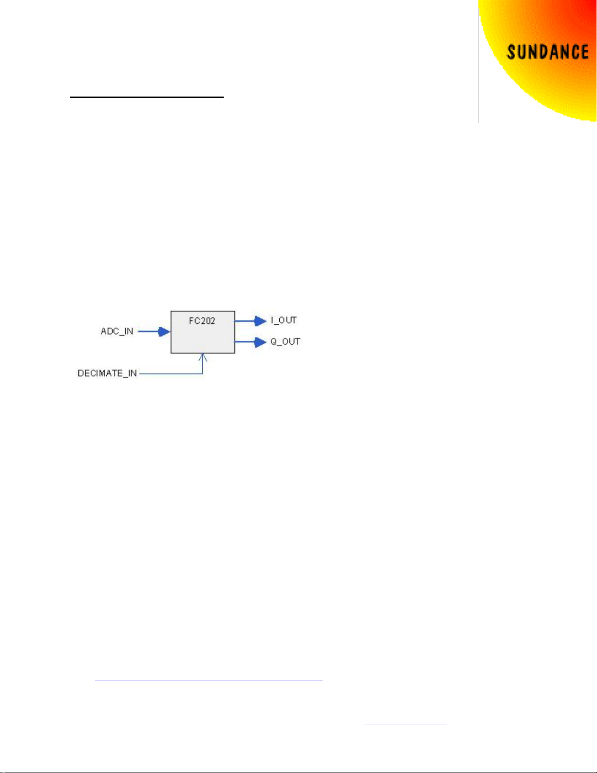
1. GENERAL DESCRIPTION
FC202 is an efficient implementation of a quadrature conversion algorithm as a 3L
Diamond FPGA task. In order for it to be used within a Diamond/FPGA system, the I/O
1
interfaces are ‘standardized’ to the model described by Diamond
.
Figure 1 – FC202 Component Diagram
1
See: http://www.3l.com/Diamond/Documentation/Diamond.pdf (Chapter 28, “FPGA Tasks”)
Sundance Digital Signal Processing Inc. Rev1.0
4790 Caughlin Parkway 233, Reno, NV 89519-0907, U.S.A.
Tel: +1 (775) 827-3103, Fax: +1 (775) 827-3664, email: sales@sundance.com
www.sundance.com
Page 7

FC202 firmware module is designed to convert a single sampled data channel into its
in-phase and quadrature components. This is useful as a pre-cursor for performing a
complex Fast Fourier Transform (FFT). This module is designed for flow-through
operation from FPGA initialization.
The module is useful for converting all types of analog data streams sampled by the Beam
Forming Reference Design hardware used by the Navy project but can equally be used in other
hardware and application scenarios. FC202 can interface and take its input from the FC201
FPGA task, which has been designed for input gain / offset correction. Details of FC201 can be
found at http://www.sundancedsp.com/edge/files/productpage.asp?STRFilter=FC201
Sundance Digital Signal Processing Inc. Rev1.0
4790 Caughlin Parkway 233, Reno, NV 89519-0907, U.S.A.
Tel: +1 (775) 827-3103, Fax: +1 (775) 827-3664, email: sales@sundance.com
www.sundance.com
Page 8

2. FC202 QUADRATURE CONVERSION
In order to interface to the FC108-D module for Polyphase filtering, a conversion from real to
quadrature representation is necessary. FC202 firmware module converts real signals to
analytic signals of In-phase and Quadrature (I & Q) components.
The method used is a linear phase conversion technique, based upon the (Parallel) Distributed
Arithmetic FIR Filter LogicCORE2. The basic approach is to approximate the Hilbert
Transform using an FIR filter3. Typically, when such methods are used, a decimate-by-2
operation can be performed without loss of spectral information. Thus, the data rate of the
outputs matches the data rate of the inputs.
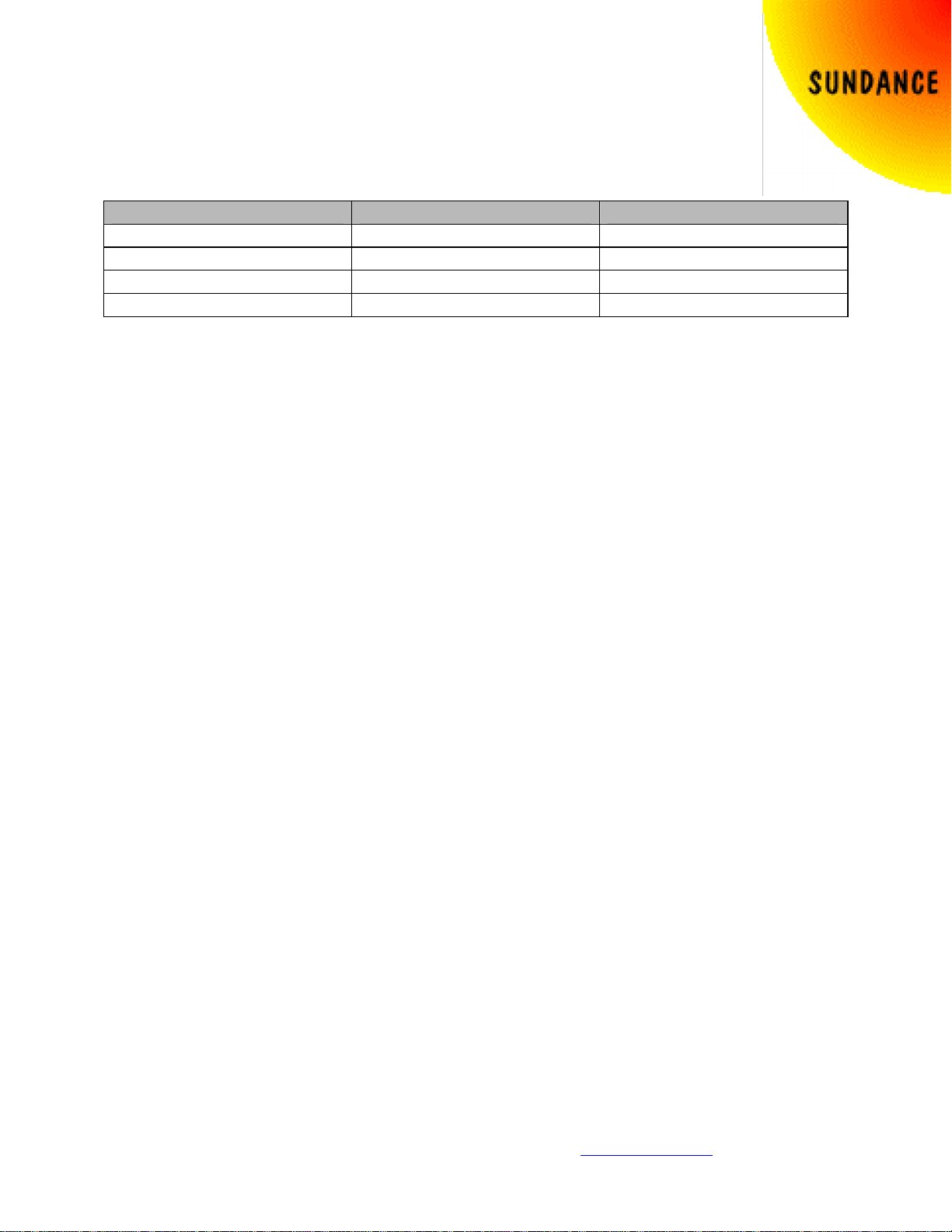
The frequency performance of the FC202 is as follows:
Sample Rate 102.4MHz
IF Center 21.4MHz
IF Bandwidth 22.5MHz
IF Span 10.15MHz –
33.65MHz
Passband (Gain=1) 5.12MHz – 46.08MHz
Table 1 - FC202 Frequency Response Characteristics
Hilbert Transform Magnitude and Phase response based on the above parameters is given in
figure 2 while figure 3 shows the XY plot of the Hilbert transform.
The FC202 component represents a pure-FPGA ‘task’, and implements the following interface:
Port Name Valid
Direction Implementation Description
Width
ADC_IN 16 Input FPGA Raw time domain data
DECIMATE_IN 1 Constant FPGA Enable decimation-by-two
I_OUT 16 Output FPGA In-Phase component, time
domain data
Q_OUT 16 Output FPGA Quadrature component, time
domain data
Table 2 - FC202 Interfaces
2
See: http://www.xilinx.com/ipcenter/catalog/logicore/docs/da_fir.pdf
3
Remez Exchange or Parks-McClellan Optimal Method
Sundance Digital Signal Processing Inc. Rev1.0
4790 Caughlin Parkway 233, Reno, NV 89519-0907, U.S.A.
Tel: +1 (775) 827-3103, Fax: +1 (775) 827-3664, email: sales@sundance.com
www.sundance.com
Page 9

Additional port descriptions are provided below:
ADC_IN
Data values are 16-bit extended twos-complement as described in the
SMT364 User Manual.
DECIMATE_IN
A bit that controls whether decimation-by-two will be performed to reduce the
data rate. (NOTE: it is anticipated that this bit will be a static-synthesis
configuration, in order to conserve FPGA resources, rather than a run-time
adjustable feature).
I_OUT
Data values are 16-bit extended twos-complement as described in the
SMT364 User Manual. This port is suitable for connecting to the FC108-D’s
I_IN port.
Q_OUT
Data values are 16-bit extended twos-complement as described in the
SMT364 User Manual. This port is suitable for connecting to the FC108-D’s
Q_IN port.
Sundance Digital Signal Processing Inc. Rev1.0
4790 Caughlin Parkway 233, Reno, NV 89519-0907, U.S.A.
Tel: +1 (775) 827-3103, Fax: +1 (775) 827-3664, email: sales@sundance.com
www.sundance.com
Page 10

Sundance Digital Signal Processing Inc. Rev1.0
4790 Caughlin Parkway 233, Reno, NV 89519-0907, U.S.A.
Tel: +1 (775) 827-3103, Fax: +1 (775) 827-3664, email: sales@sundance.com
www.sundance.com
Page 11

Figure 2 - Typical System Integration Model
Sundance Digital Signal Processing Inc. Rev1.0
4790 Caughlin Parkway 233, Reno, NV 89519-0907, U.S.A.
Tel: +1 (775) 827-3103, Fax: +1 (775) 827-3664, email: sales@sundance.com
www.sundance.com
Page 12

Figure 3 - Hilbert Transform Magnitude and Phase Response
Figure 4 - XY Plot of Hilbert Transform
Sundance Digital Signal Processing Inc. Rev1.0
4790 Caughlin Parkway 233, Reno, NV 89519-0907, U.S.A.
Tel: +1 (775) 827-3103, Fax: +1 (775) 827-3664, email: sales@sundance.com
www.sundance.com
Page 13

3. PRESENTATION
The firmware module is instantiated in a Diamond/FPGA configuration as follows:
FC202_ea1\
+---analysis\ Implematation Analysis
+---FC202\ Task Source Code
+---fifo\ Shared fifo tasks for test
+---simulink\ Simulink model Test Benches for FC202
+---simulation\ VHDL Test Benches
+---Specifications\ Documentation
+---test \ Verification Test Benches
Users of the FC202 firmware module will reference the Diamond .fcd file (top level) from the
FC202\ above.
Note: In the deliverable hierarchy in each folder a Reademe.txt is provided to briefly describe
the files included.
Sundance Digital Signal Processing Inc. Rev1.0
4790 Caughlin Parkway 233, Reno, NV 89519-0907, U.S.A.
Tel: +1 (775) 827-3103, Fax: +1 (775) 827-3664, email: sales@sundance.com
www.sundance.com
Page 14

4. USAGE
The firmware module is instantiated in a Diamond//FPGA configuration file as follows:
! declare tasks
!
task ogdl ins=1 outs=2 file”..\fc202\fc202.fcd”
!
! place tasks on FPGA
!
place ogdl <fpga>
!
!
!
Connect ? <user_1>[0] ogdl[0]
Connect ? ogdl[0] <user_2>[0]
Connect ? ogdl[1] <user_2>[1]
Where <user_1> is a data source and <user_2> is a data sink task.
In most cases, it is useful to provide some amount of elastic buffering before and after the
FC202 task in order to help close timings in the FPGA design. This can be accomplished as
follows:
! declare tasks
!
task fifo1 ins=1 outs=1 file”..\fifo\fifo.fcd”
task ogdl ins=1 outs=2 file”..\fc202\fc202.fcd”
task fifo2 ins=1 outs=1 file”..\fifo\fifo.fcd”
task fifo3 ins=1 outs=1 file”..\fifo\fifo.fcd”
!
! place tasks on FPGA
!
place fifo1 <fpga>
place ogdl <fpga>
place fifo2 <fpga>
place fifo3 <fpga>
!
!
!
Connect C1 <user_1>[0] fifo1[0]
Sundance Digital Signal Processing Inc. Rev1.0
4790 Caughlin Parkway 233, Reno, NV 89519-0907, U.S.A.
Tel: +1 (775) 827-3103, Fax: +1 (775) 827-3664, email: sales@sundance.com
www.sundance.com
Page 15

Connect ? fifo1[0] ogdl[0]
Connect ? ogdl[0] fifo2[0]
Connect C2 fifo2[0] <user_2>[0]
Connect ? ogdl[1] fifo3[0]
Connect C3 fifo3[1] <user_2>[1]
Sundance Digital Signal Processing Inc. Rev1.0
4790 Caughlin Parkway 233, Reno, NV 89519-0907, U.S.A.
Tel: +1 (775) 827-3103, Fax: +1 (775) 827-3664, email: sales@sundance.com
www.sundance.com
Page 16

5. VERFICATION
The firmware module is supported by PARS Test Benches targeted on a mixed DSP + FPGA
module SMT365_8_1, to validate the functionality of the core.
Note: The PARS based verification models generates Diamond configuration files and
applications files. These configuration files can also be used independently without PARS, to
generate Diamond applications. The test benches included under ..\fc202_ea1\test\ will reflect
this in the next release.
DSP Test Bench
A Simulink model of the FC202 core is implemented. The C reference model is generated
using PARS to target the SMT365_8_1 DSP. The Simulink model “fc202_dsp.mdl” is located
under:
..\fc202_ea1\simulink\fc202_dsp\
Note: Please refer to PARS user guide to generate the code to target DSP’s from Simulink
models.
The PARS generated test bench “Subsystem2_TestBench.mdl” is located under
..\fc202_ea1\simulink\fc202_dsp\fc202_dsp_PARS\
Executing the test bench will load the “fc202_dsp_pars.app” into the SMT365_8_1 DSP and
display a scope with the In-phase and Quadrature waveforms of the input samples. Figure 5
below shows the In-Phase and Quadrature waveforms generated by the test bench.
In order to change the Target DSP, a new hardware profile needs to be created in the file
“get_hi.m”. This file is located under PARS directory C:\SundanceDSP\PARS\PARS.
Please refer to PARS user guide for instructions on how to update the “get_hi.m” file.
FPGA Test Bench
A Simulink model “fc202_fpga.mdl” is generated using both Simulink blocks and FC202 core
block. The FC202 block is generated using the “CPBT” utility available under PARS.
The model “fc202_fpga.mdl” is located under
Sundance Digital Signal Processing Inc. Rev1.0
4790 Caughlin Parkway 233, Reno, NV 89519-0907, U.S.A.
Tel: +1 (775) 827-3103, Fax: +1 (775) 827-3664, email: sales@sundance.com
www.sundance.com
Page 17

..\fc202_ea1\simulink\fc202_fpga\
Figure 5 - In-Phase and Quadrature output generated by DSP model
The PARS generated test bench “Subsystem2_TestBench.mdl” can be found under
..\fc202_ea1\simulink\fc202_dsp\fc202_dsp_PARS\
Figure 6 below shows the results generated by the actual core executed on an FPGA.
The delay in the In-Phase signal is due to the hardware delay. This cannot be seen in the DSP
model above as the Hilbert transform component is implemented only for the Quadrature
output.
Sundance Digital Signal Processing Inc. Rev1.0
4790 Caughlin Parkway 233, Reno, NV 89519-0907, U.S.A.
Tel: +1 (775) 827-3103, Fax: +1 (775) 827-3664, email: sales@sundance.com
www.sundance.com
Page 18

Integrity Test Bench
The integrity test bench is basically a combination of both the DSP and FPGA test
bench included in a single model.
The model “fc202_integrity.mdl” is located under
..\fc202_ea1\simulink\fc202_integrity\
Figure 6 - In-Phase and Quadrature output generated by FPGA model
Executing the integrity test bench will generate the results shown in Figure 7.
Sundance Digital Signal Processing Inc. Rev1.0
4790 Caughlin Parkway 233, Reno, NV 89519-0907, U.S.A.
Tel: +1 (775) 827-3103, Fax: +1 (775) 827-3664, email: sales@sundance.com
www.sundance.com
Page 19

Figure 7 - Integrity Test Bench results
Sundance Digital Signal Processing Inc. Rev1.0
4790 Caughlin Parkway 233, Reno, NV 89519-0907, U.S.A.
Tel: +1 (775) 827-3103, Fax: +1 (775) 827-3664, email: sales@sundance.com
www.sundance.com
Page 20

6. RELEASE NOTES
1) Decimate by two function has not been implemented in the present release. Will be
implemented in the next release.
2) Test benches (fc202_mdl.app, fc202_unit.app, fc202_integrity.app) under
..\fc202_ea1\test\ are under development.
3) VHDL simulation of the FC202 core is not included in this release.
7. DELIVERABLES
FC202 is a complete Diamond/FPGA firmware module that includes:
• Firmware source (.vhd) files
• Diamond/FPGA integration support (.fcd, _pkg.vhd) and example implementation
• Simulation harness
• Matlab analysis tools
• User Guide
8. LICENSING AND PROPERTY RIGHTS
Sundance DSP retains copyright and licensing rights, and distributes the FC202 firmware
module under non-disclosure agreement only. Special arrangements are made on a case-bycase basis.
In order to obtain updates and technical support for the FC202 firmware module all customers
need to purchase an annual support contract from Sundance DSP.
For support please register on http://support.sundance.com
and post all questions on the forum.
You can also contact any of Sundance offices, around the world, by telephone or email. For
details please see Sundance web site at www.sundance.com
Sundance Digital Signal Processing Inc. Rev1.0
4790 Caughlin Parkway 233, Reno, NV 89519-0907, U.S.A.
Tel: +1 (775) 827-3103, Fax: +1 (775) 827-3664, email: sales@sundance.com
www.sundance.com
 Loading...