

Page 1

FC201 - General Offset/Gain/Delay Correction
FPGA Core
User’s Guide
Copyright © Sundance DSP Inc.
All rights reserved. No part of this document may be reproduced, translated,
stored in a retrieval system, or transmitted, in any form or by any means,
electronic, mechanical, photocopying, recording or otherwise, without prior
written permission of the owner.
Note:
If this copy is no longer in use, return to sender.
Page 2
Page 2 of 2
Revision 0.4
AUTHORS
Name Signature Date
B. Vacaliuc 19-May-07
DOCUMENT HISTORY
Date Initials Revision Description of Change
1-May-07 BV 0.1 Initial Release
Table of Contents
1. GENERAL DESCRIPTION...................................................................................................2
2. FEATURES ............................................................................Error! Bookmark not defined.
3. THEORY OF OPERATION ..................................................Error! Bookmark not defined.
4. I/O DESCRIPTION, BASIC MODULE................................Error! Bookmark not defined.
5. I/O DESCRIPTION, DIAMOND MODULE.........................Error! Bookmark not defined.
6. PRESENTATION...................................................................Error! Bookmark not defined.
7. USAGE ...................................................................................Error! Bookmark not defined.
8. VERIFICATION ....................................................................Error! Bookmark not defined.
9. DELIVERABLES...................................................................Error! Bookmark not defined.
10. LICENSING AND PROPERTY RIGHTS.............................Error! Bookmark not defined.
11. ORDERING INFORMATION...............................................Error! Bookmark not defined.
Table of Figures
Figure 1 - Component Diagram.......................................................................................................3
Figure 2 - Typical System Integration Model..................................................................................9
Sundance Digital Signal Processing Inc.
4790 Caughlin Parkway 233, Reno, NV 89519-0907, U.S.A.
Tel: +1 (775) 827-3103, Fax: +1 (775) 827 -3664, email: sales@sundancedsp.com
www.sundancedsp.com
Page 3
Page 3 of 3
Revision 0.4
1. GENERAL DESCRIPTION
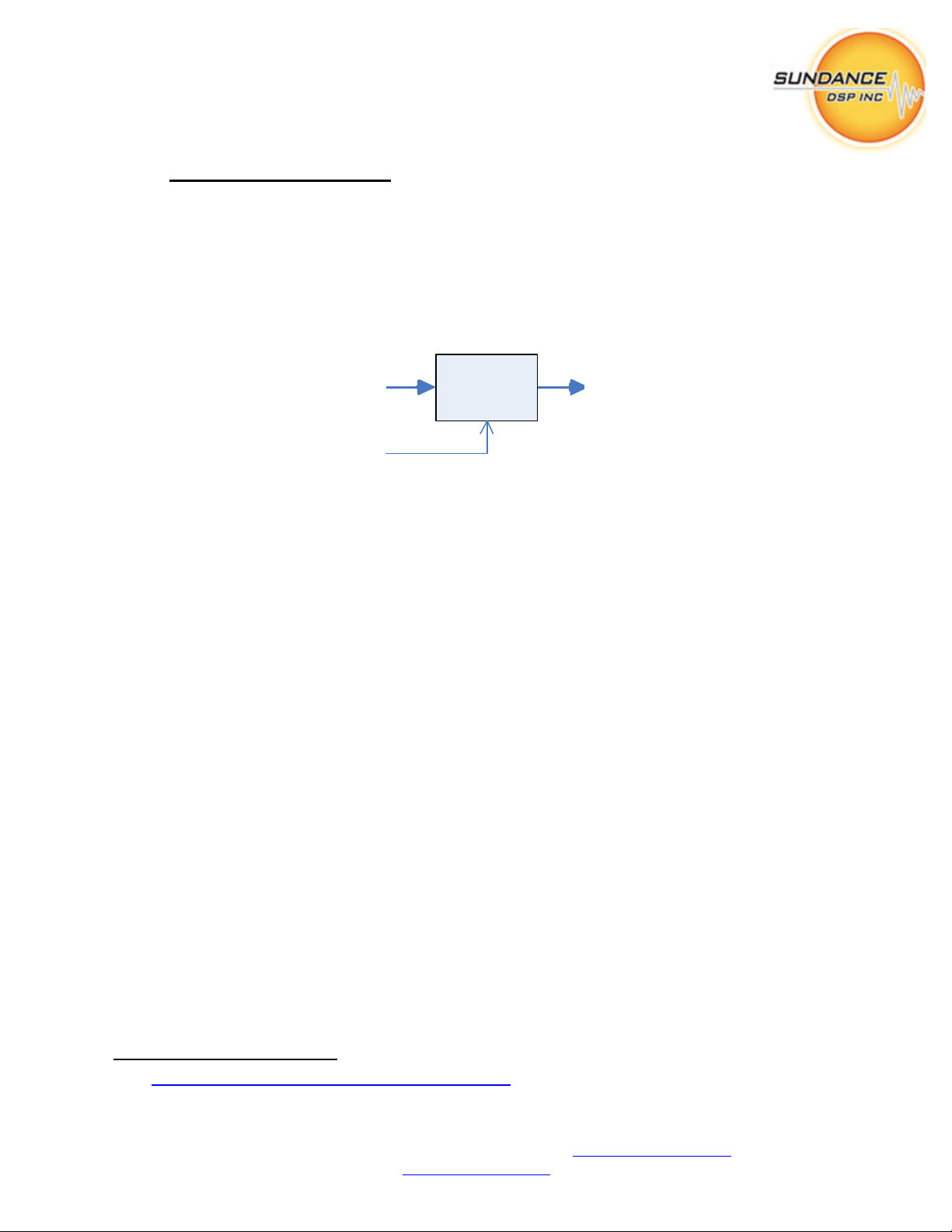
This document describes the specifications of a 3L Diamond/FPGA firmware module.
The FC201 is an efficient implementation of a general offset/gain/delay correction. In order for
it to be used within a Diamond/FPGA system, the I/O interfaces are ‘standardized’ to the model
described by Diamond1.
FC201
ADC_OUTADC_IN
COEFF_IN
Figure 1 - Component Diagram
The firmware module operates in a flow-through mode; for every ADC_IN sample written, one
ADC_OUT sample will be clocked out.
The FC201 firmware module is designed to correct a single digital data channel. Typically, each
channel requires its own correction coefficients. Coefficients are loaded asynchronously and are
applied prior to the next input cycle. Loading coefficients affects a reset of the module. The
module will not accept ADC_IN samples until the first set of coefficients are loaded.
The module is useful for correcting ADC input as well as DAC output data streams.
1
See: http://www.3l.com/Diamond/Documentation/Diamond.pdf (Chapter 28, “FPGA Tasks”)
Sundance Digital Signal Processing Inc.
4790 Caughlin Parkway 233, Reno, NV 89519-0907, U.S.A.
Tel: +1 (775) 827-3103, Fax: +1 (775) 827 -3664, email: sales@sundancedsp.com
www.sundancedsp.com
Page 4

Page 4 of 4
Revision 0.4
2. PRESENTATION
The firmware module is instantiated in a Diamond/FPGA configuration file as follows:
FC201\
+---analysis\ Implementation Analysis
+---fc201\ Task Source Code
+---fifo\ Shared FIFO Tasks for test\
+---specifications\ Documentation
\---test\ Verification Test Benches
Users of the FC201 firmware module will reference the Diamond .fcd file (top level) from the
fc201\ above.
3. USAGE
The firmware module is instantiated in a Diamond/FPGA configuration file as follows:
! declare tasks
!
task ogd1 ins=2 outs=1 file="..\fc201\fc201.fcd"
!
! place tasks on FPGA
!
place ogd1 <fpga>
!
! connect dataflow
!
connect ? <user_1>[x] ogd1[0]
connect ? <user_cfg>[y] ogd1[1]
connect ? ogd1[0] <user_2>[z]
Where <user_1> is a data source and <user_2> is a data sink task. <user_cfg> is a
connection which supplies 3-word tuples to configure the coefficients.
Sundance Digital Signal Processing Inc.
4790 Caughlin Parkway 233, Reno, NV 89519-0907, U.S.A.
Tel: +1 (775) 827-3103, Fax: +1 (775) 827 -3664, email: sales@sundancedsp.com
www.sundancedsp.com
Page 5

Page 5 of 5
Revision 0.4
In most cases, it is useful to provide some amount of elastic buffering before and after the FC201
task in order to help close timing in the FPGA design. This can be accomplished as follows:
! declare tasks
!
task fifo1 ins=1 outs=1 file="..\fifo\fifo8.fcd"
task ogd1 ins=2 outs=1 file="..\fc201\fc201.fcd"
task fifo2 ins=1 outs=1 file="..\fifo\fifo8.fcd"
!
! place tasks on FPGA
!
place fifo1 <fpga>
place ogd1 <fpga>
place fifo2 <fpga>
!
! connect dataflow
!
connect C1 <user_1>[x] fifo1[0]
connect ? fifo1[0] ogd1[0]
connect C2 <user_cfg>[y] ogd1[1]
connect ? ogd1[0] fifo2[0]
connect C3 fifo2[0] <user_2>[z]
Note: When implementing on some FPGA devices, a slower clock may be needed.
In order to close timing on some (slow) FPGA device/speed grades, the task may need to run
under a slower clock. To do this, use Diamond's facility to generate a custom clock, and provide
this clock to each FC201 instance.
See the 3L/Diamond User Guide v3.1.3 pg. 306 for additional details.
For example:
! Use a slower clock for the UUT
!
clock slow processor=<fpga> source=DEFAULT output=50MHz
!
! place tasks on FPGA
!
place ogd1 <fpga> clock=slow
Sundance Digital Signal Processing Inc.
4790 Caughlin Parkway 233, Reno, NV 89519-0907, U.S.A.
Tel: +1 (775) 827-3103, Fax: +1 (775) 827 -3664, email: sales@sundancedsp.com
www.sundancedsp.com
Page 6

Page 6 of 6
Revision 0.4
4. VERIFICATION
The firmware module is currently supported by two types of test benches. In all cases,
compilation is performed using gmake (distributed with CCS3.0 or greater)2.
Unit Test Benches
A C- Reference Model is implemented as a Diamond/DSP Task. This model produces a bitexact representation of the operations performed by the FPGA task. The code is as follows
(provided in fc201\fc201_mdl.c):
uint32_t in, out;
int32_t d0_q15p0;
int64_t d1_q16p16;
int64_t d2_q31p32;
int32_t d3_q15p0;
d0_q15p0 = (signed)(in & 0xFFFF);
d1_q16p16 = (d0_q15p0<<16) + offset_q15p16
d2_q31p32 = d1_q16p16 * gain_q15p16
d3_q15p0 = (int32_t)( d2_q31p32 >> 32 );
if( (d2_q31p32>>31) & 1 )
d3_q15p0 += (d2_q31p32 < 0) ? -1 : 1
if( d3_q15p0 > SHRT_MAX ) d3_q15p0 = SHRT_MAX
else if( d3_q15p0 < SHRT_MIN ) d3_q15p0 = SHRT_MIN;
out = (uint32_t)d3_q15p0;
This implementation of this model also correctly accounts for the pipeline depth (4 samples)
which is observed at the output (this is above any additional delay samples introduced by the
delay coefficient).
Applications are provided to perform unit tests on the C reference as well as the FPGA
implementation on a supported DSP module (the C reference model executes on the DSP, while
the FPGA implementation executes on the FPGA attached to the DSP).
To use the test benches, use ProcType.exe to define the DEFAULT processor type for your
3L/Diamond hardware platform. Be sure to select a supported “hybrid” DSP/FPGA module,
such as the SMT365-8-2, etc. Execute the fc201_mdl.app, and fc201_unit.app. This
2
Only gmake has the necessary syntax to effectively implement the build system. Contact Sundance DSP for
assistance if your installation lacks CCS.
Sundance Digital Signal Processing Inc.
4790 Caughlin Parkway 233, Reno, NV 89519-0907, U.S.A.
Tel: +1 (775) 827-3103, Fax: +1 (775) 827 -3664, email: sales@sundancedsp.com
www.sundancedsp.com
Page 7

Page 7 of 7
Revision 0.4
will generate the files ‘output_FC201m.dat' and 'output_FC201u.dat' files
respectively. These files should be IDENTICAL.
Next, execute the fc201_integrity.app. This application generates test vectors
continuously, providing the same data to both the FPGA implementation and the C-Reference
model. The resulting output is compared to ensure a bit-exact operation. This test bench can
execute indefinitely to ensure coverage of all input byte codes.
Resource and Performance Analysis Benches
A mechanism to obtain the resource utilization of the FC201 core is provided. The basic
principle is to generate a “baseline” implementation of the target FPGA that contains a ‘stub’.
The ‘stub’ has all the same inputs and outputs, but is a trivial implementation of the FPGA task.
This “baseline” is compared to a real instantiation of the FC201 module. The stub FPGA task is
provided as ‘fc201\fc201_base.fcd’.
Comparing the two MAP report files and subtracting the Slices, BRAM and MPY in use
provides an accurate real-word estimate of the resources used by the FC201 module.
Finally, Diamond application configuration files are provided which enable the FC201 module to
be instantiated into a supported single (stand-alone) FPGA board. By connecting the dataflow
inputs (ADC_IN and ADC_OUT) of the FC201 to SDB resources, and the COEFF_IN to the
default Comport (CP3, typically) resource, a hardware reference is created which can be added to
any system and operated at line rate.
The configuration files and makefile for accomplishing these are provided in the analysis\
folder.
5. FC201 – ADC/DAC Calibration
A calibration operation is required to normalize the output of each ADC/DAC (DAQ) within a
multi -DAQ system. Variations in the manufacturing process of the DAQs and the surrounding
circuitry can introduce voltage offsets and sampling gain variations on each channel. Further,
external systems connected to the DAQs may not have complete control over all process
parameters. Finally, when acquiring signals among multiple channels and multiple boards,
(fixed) delays in the sampling clock may occur.
Each FC201 instance allows any digital data channel to be corrected at the rate that the data is
produced. It acts as a ‘digital filter’ to transform the data stream. The FC201 component can
manipulate samples in magnitude and time. It is the responsibility of the end-user application to
determine the appropriate coefficients provided to the FC201 component in order to operate
properly.
Sundance Digital Signal Processing Inc.
4790 Caughlin Parkway 233, Reno, NV 89519-0907, U.S.A.
Tel: +1 (775) 827-3103, Fax: +1 (775) 827 -3664, email: sales@sundancedsp.com
www.sundancedsp.com
Page 8

Page 8 of 8
Revision 0.4
The FC201 component presents as a pure-FPGA ‘task’, and implements the following interface:
Port Name Valid
Direction Implementation Description
Width
ADC_IN 16 Input FPGA Real time domain data
COEFF_IN
32 Input FPGA Coefficient tuple load {offset, gain,
delay)
ADC_OUT 16 Output FPGA Corrected, saturated, delayed, real time
domain data
Table 1 - FC201 Interfaces
Additional port descriptions are provided below:
ADC_IN
Data values are 16-bit extended twos-complement. Only bits (15 downto 0)
are significant, higher order bits are ignored.
COEFF_IN
Data values are accepted as a 3-word tuple: offset, gain and sample delay.
The data format for offset/gain is Q15.16 (signed, 15-bit integer, 16-bit
fractional)3. The format for delay is an unsigned 4-bit integer, representing an
amount of sample delay. Loading coefficients causes a reset of the module.
ADC_OUT
Data values are 16-bit extended twos-complement. The values saturate to
+32767/-32768 as part of the offset/gain operation. If a non-zero delay is
given, the output samples will be taken from a 16-tap shift-register. The
higher-order output bits (31 downto 16) are sign extended from bit 15.
5.1. System Integration Considerations
The DAQ calibration ‘tasks’ are placed on the FPGA hosting the channel capture. This FPGA
needs to be supported by Diamond/FPGA in order for the tasks to be integrated.
MODULE FPGA Slices BRAM MPY F
Notes
MAX
3
See: http://en.wikipedia.org/wiki/Fixed-point_arithmetic, “Fixed Point Nomenclature”,
http://www.superkits.net/whitepapers/Fixed%20Point%20Representation%20&%20Fractional%20Math.pdf, and
http://focus.ti.com/lit/ug/spru565b/spru565b.pdf (appendix A.2)
Sundance Digital Signal Processing Inc.
4790 Caughlin Parkway 233, Reno, NV 89519-0907, U.S.A.
Tel: +1 (775) 827-3103, Fax: +1 (775) 827 -3664, email: sales@sundancedsp.com
www.sundancedsp.com
Page 9

Page 9 of 9
1 4
1 4
Revision 0.4
SMT348-10 XC4VSX55-10
SMT365-8-1 XC2V1000-4 173
SMT368-10 XC4VSX35-10
SMT368-12 XC4VSX35-12
SMT398-8000 XC2V8000-4 173
SMT398-VP70 XC2VP70-6
SMT417 XC2VP50-5
51.92MHz Unit Test on DSP Module
51.92MHz Extrapolated from XC2V1000-4
Table 2 – FC201 Performance Estimates and Resource Utilization
Exceeding F
will cause flow-control logic to come into play and back-up the input data all
MAX
the way to the source. It is the system designer’s responsibility to handle this condition.
SMT368
Board 1
SMT384
CH1
CH2
SMT368
A(I)
FC201
I
A(Q) FC201
Q
COEFF_IN
B(I)
FC201
I
B(Q) FC201
Q
COEFF_IN
C(I)
FC201
C(Q)
COEFF_IN
D(I)
D(Q)
COEFF_IN
I
FC201
Q
FC201
I
FC201
Q
SMT368
Board 2
CH3
CH4
Figure 2 - Typical System Integration Model
Sundance Digital Signal Processing Inc.
4790 Caughlin Parkway 233, Reno, NV 89519-0907, U.S.A.
Tel: +1 (775) 827-3103, Fax: +1 (775) 827 -3664, email: sales@sundancedsp.com
www.sundancedsp.com
Page 10

Page 10 of 10
Revision 0.4
6. DELIVERABLES
FC201 is a complete Diamond/FPGA firmware module that includes:
?? Firmware source (.vhd) files
?? Diamond/FPGA integration support (.fcd, _pkg.vhd) and example implementation s
?? Simulation harness [NOTE: Not available in Release 0.1]
?? Matlab analysis tools [NOTE: Not available in Release 0.1]
?? User Guide
7. LICENSING AND PROPERTY RIGHTS
Sundance DSP retains copyright and licensing rights, and distributes the FC201 firmware
module under non-disclosure agreement only. Special arrangements are made on a case-by-case
basis.
All customers need to purchase support contracts from Sundance DSP in order to be able to
obtain updates and technical support for the FC201 firmware module.
8. ORDERING INFORMATION
The FC201 component may be ordered separately, or bundled with a cores package containing
multiple cores. Contact Sundance DSP for specific details.
Sundance Digital Signal Processing Inc.
4790 Caughlin Parkway 233, Reno, NV 89519-0907, U.S.A.
Tel: +1 (775) 827-3103, Fax: +1 (775) 827 -3664, email: sales@sundancedsp.com
www.sundancedsp.com
 Loading...