

TM-8105005042
Solid State Kilowatt
Linear Power Amplifier
LPA-9600
Operation and Maintenance Manual (Rev. D)
WARNING
The LPA-9600 ships with internal packing material.
You MUST open the top cover and remove the
packing material BEFORE operating the unit.
3131 SW 42nd Street, Fort Lauderdale, Florida 33312 U.S.A.
www.sunairelectronics.com

LPA-9600
ii Use or disclosure of information from this document is subject to the restrictions
Proprietary/Confidentiality Notice
The information disclosed in this document, including all designs and related materials, is the property of
RIIMIC LLC dba (doing business as) Sunair Electronics (hereinafter “Sunair”) and/or its licensors. Sunair
and/or its licensors reserve all patent, copyright, and other proprietary rights to this document, including
all design, manufacturing, reproduction, use, and sales rights thereto, except to the extent said rights are
expressly granted to others. Reproduction of this document or portions thereof without prior written
approval of Sunair is prohibited.
Return Material Authorization (RMA) Procedures
In case of difficulty, please contact the Sunair Product Service Department between the hours of 8:00 a.m.
and 5:00 p.m. EST.
Telephone: (954) 400-5100
Fax: (954) 583-7337
Email: techsupport@sunairelectronics.com
To return an item for repair or replacement, a Return Material Authorization (RMA) is required from the
Product Service Department. When you receive the RMA number, carefully pack the item(s) and ship the
package(s) to the address provided by your Product Service Representative.
Write the RMA number in a visual location on the outside of the shipping container.
Retain a copy of all information sheets included with the packaging.

LPA-9600
Use or disclosure of information from this document is subject to the restrictions iii
Warranty Policy
Ground and Marine Products
Sunair Electronics warrants each piece of equipment manufactured by it to be free from defects in
material and workmanship, under normal use for the lesser of one year from the date of installation or 15
months from the date of shipment from Sunair.
Sunair will repair or replace, at its option, any defective equipment or component of the equipment
returned to it at its factory, transportation prepaid, within such warranty period. No reimbursement will be
made for non-factory repair charges.
This warranty is void if equipment is modified or repaired without authorization, subject to misuse, abuse,
accident, water damage or other neglect, or has its serial number defaced or removed.
THIS WARRANTY IS ESPECIALLY IN LIEU OF ANY AND ALL OTHER WARRANTIES
EXPRESSED OR IMPLIED, INCLUDING ANY IMPLIED WARRANTY OF MERCHANTABILITY
OR FITNESS FOR A PARTICULAR PURPOSE. The obligation and responsibility of Sunair shall be
limited to that expressly provided herein and Sunair shall not be liable for consequential or other damage
or expense whatsoever therefore or by any reason thereof.
Sunair reserves the right to make changes in the design or additions to or improvements in its equipment
without obligation to install such additions or improvements in equipment theretofore manufactured.
Training
Sunair offers training programs of varying lengths covering operation, service and maintenance of all
Sunair manufactured equipment. For details please contact the Product Service Department.
LPA-9600
iv Use or disclosure of information from this document is subject to the restrictions
Copyright © 2011, 2012 by Sunair Electronics
All rights reserved.
Printed in the United States of America
Revision
Page(s)
Manual
Revision
Date
Unit Serial No.
Effectivity
Addendum
Covered
A - First Edition - Production Changes
10/01/1990
B - Second Edition - Customer
Changes
8/29/2005
C - Third Edition
3/01/2011
N/A
N/A
• Reformatted LPA-9600 to current
standards. This includes new
numbers for Figures and Tables.
• Added temperatures in Fahrenheit.
• Replaced references to CU-9100
with CU-9150.
All
• Incorporated Service Bulletin
9600-001.
1-1, 1-2, 3-2, 5-
1, 5-2, 5-26
• Re-created several of the handdrawn diagrams using illustrating
software.
1-4, 2-3, 2-5, 2-
6, 2-8, 2-9, 4-
19, 5-22, 5-27,
5-28, 5-31, 5-
32
• Updated the contact information
with the new address and phone
numbers.
I, ii, 2-1
• Paragraph 5.5.1.1, step 3,
changed:
- +12 VDC to + 5 VDC
- A4J1 to + A4A1J4
5-10
Revised BOM for Power Amplifier
A4A3
5-49
D - Revision
02/26/2013
N/A
N/A
• Modified Rackmount Slide
Diagram (Figure 2.9-1)
2-13
• Modified Captions
All
• Modified General Glossary
xiii & xiv
• Modified CU-9150 Instructions
2-10

LPA-9600
Table of Contents
Use or disclosure of information from this document is subject to the restrictions v
1.0! General Information ............................................................................................................................ 1-1!
1.1! Purpose of Manual ..................................................................................................................... 1-1!
1.2! Purpose of Equipment ............................................................................................................... 1-1!
1.3! General Description ................................................................................................................... 1-1!
1.3.1! Physical Description ..................................................................................................... 1-1!
1.3.2! Electrical Description ................................................................................................... 1-1!
1.4! Specifications ............................................................................................................................ 1-2!
1.5! Dimensions ................................................................................................................................ 1-3!
1.6! Equipment Supplied .................................................................................................................. 1-6!
1.7! Equipment Required, Not Supplied ........................................................................................... 1-6!
1.8! Optional Equipment ................................................................................................................... 1-7!
2.0! Installation ........................................................................................................................................... 2-1!
2.1! General ...................................................................................................................................... 2-1!
2.2! Unpacking and Inspection ......................................................................................................... 2-1!
2.3! Returning Equipment to Factory ............................................................................................... 2-2!
2.4! General Installation Information ............................................................................................... 2-2!
2.4.1! Station Layout .............................................................................................................. 2-2!
2.5! Configurations ........................................................................................................................... 2-3!
2.6! Antennas and Ground Systems .................................................................................................. 2-3!
2.6.1! Random Length Non-Resonant Antennas .................................................................... 2-3!
2.6.2! Broadband 50 Ohm Antennas ...................................................................................... 2-3!
2.7! External Connections ................................................................................................................. 2-8!
2.7.1! Primary Power Connections ......................................................................................... 2-8!
2.7.2! Transceiver Connections .............................................................................................. 2-8!
2.7.3! RF Output Connections ................................................................................................ 2-8!
2.7.4! Antenna Coupler Connections ................................................................................... 2-10!
2.7.5! Station RF Ground System Connections .................................................................... 2-10!
2.8! Preliminary Checks and Adjustments ..................................................................................... 2-10!
2.9! Rack Mounting Kit Option ...................................................................................................... 2-12!
3.0! Operation ............................................................................................................................................. 3-1!
3.1! General ...................................................................................................................................... 3-1!
3.2! Function and Location of Controls and Indicators .................................................................... 3-1!
3.3! Operating the LPA-9600 ........................................................................................................... 3-3!
3.3.1! Operation with a 9000 Series Exciter/Transceiver ....................................................... 3-3!
4.0! Theory of Operation ............................................................................................................................ 4-1!
4.1! General ...................................................................................................................................... 4-1!
4.2! Control Panel Module A2 .......................................................................................................... 4-1!
4.3! Computer Assembly A3 ............................................................................................................ 4-2!

LPA-9600
Table of Contents
vi Use or disclosure of information from this document is subject to the restrictions
4.3.1! PC Assembly Computer Mother Board A3A1 ............................................................. 4-2!
4.3.2! Peripheral Board A3A2 ................................................................................................ 4-2!
4.3.3! Microprocessor Board A3A3 ....................................................................................... 4-8!
4.4! RF/PS Module A4 ................................................................................................................... 4-13!
4.4.1! RF Module Control Assembly A4A1 ......................................................................... 4-13!
4.4.2! +48 VDC Switching Power Supply A4A2 ................................................................. 4-13!
4.4.3! Power Amplifier Assembly A4A3 ............................................................................. 4-15!
4.5! Filter Module A5 ..................................................................................................................... 4-16!
4.5.1! Plug-In Filter Modules A5A1 Through A5A8 ........................................................... 4-16!
4.5.2! Plug-In Wattmeter Module A5A9 .............................................................................. 4-16!
4.5.3! Mother Board Assembly A5A10 ................................................................................ 4-17!
4.6! Output Power Combiner A6 .................................................................................................... 4-17!
4.7! Input Power Splitter Assembly A7 .......................................................................................... 4-17!
4.8! Front Panel A8 ......................................................................................................................... 4-17!
4.9! Rear Panel Connector Assembly A9 ....................................................................................... 4-17!
4.10! Auxiliary Power Supply A10 .................................................................................................. 4-17!
4.11! Block Diagrams ....................................................................................................................... 4-18!
5.0! Fault Isolation, Maintenance, and Repair ............................................................................................ 5-1!
5.1! Preventive Maintenance ............................................................................................................ 5-1!
5.1.1! Periodic Inspections ..................................................................................................... 5-1!
5.2! Corrective Maintenance ............................................................................................................. 5-1!
5.2.1! Test Equipment Required ............................................................................................. 5-1!
5.2.2! Connectors and Cables Required ................................................................................. 5-2!
5.2.3! Primary Power Input .................................................................................................... 5-2!
5.2.4! Test Conditions ............................................................................................................ 5-2!
5.3! Alignment Procedures ............................................................................................................... 5-2!
5.3.1! Preliminary ................................................................................................................... 5-2!
5.3.2! Power Up ...................................................................................................................... 5-2!
5.3.3! Keyboard ...................................................................................................................... 5-3!
5.3.4! Power Adjustment ........................................................................................................ 5-3!
5.3.5! 500 Watt Adjustment ................................................................................................... 5-4!
5.3.6! AM Power .................................................................................................................... 5-4!
5.3.7! VSWR Adjustment ....................................................................................................... 5-5!
5.4! Fault Messages .......................................................................................................................... 5-5!
5.5! Fault Isolation Procedures ....................................................................................................... 5-10!
5.5.1! RF/PS Module A4 ...................................................................................................... 5-10!
5.5.2! Peripheral Board A3A2 .............................................................................................. 5-10!
5.5.3! Filter Module A5 ........................................................................................................ 5-10!
5.5.4! Output Combiner A6 .................................................................................................. 5-11!

LPA-9600
Table of Contents
Use or disclosure of information from this document is subject to the restrictions vii
5.5.5! Input Splitter A7 ......................................................................................................... 5-11!
5.5.6! Microprocessor Board A3A3 ..................................................................................... 5-11!
5.6! Disassembly Instructions ......................................................................................................... 5-11!
5.7! Major Assembly Locations ...................................................................................................... 5-12!
5.8! Schematics and Parts Lists ...................................................................................................... 5-23!

LPA-9600
Table of Contents
viii Use or disclosure of information from this document is subject to the restrictions
THIS PAGE INTENTIONALLY LEFT BLANK

LPA-9600
List of Figures
Use or disclosure of information from this document is subject to the restrictions ix
Figure 1.5-1: LPA-9600 Outline and Mounting Dimensions .................................................................... 1-4!
Figure 1.5-2: LPA-9600 Front and Rear Panels ........................................................................................ 1-5!
Figure 2.6-1: LPA-9600 with Broadband Antenna .................................................................................... 2-4!
Figure 2.6-2: LPA-9600 with CU-9150, 35-Foot Antenna (Roof Top Installation) ................................. 2-5!
Figure 2.6-3: LPA-9600 with CU-9150, Non-Resonant Antenna ............................................................. 2-6!
Figure 2.6-4: kW Long Wire Antenna Kit ................................................................................................. 2-7!
Figure 2.7-1: Power Cable Assembly, P/N 8066002297 ........................................................................... 2-8!
Figure 2.7-2: 9000 Series Exciter/Transceiver to LPA-9600 Control Cable ............................................. 2-9!
Figure 2.8-1: Voltage Customizing - Circuit Breaker/Auxiliary Power Supply ..................................... 2-11!
Figure 2.8-2: Voltage Customizing – RF/PS Module A4 (4 Each) ......................................................... 2-12!
Figure 2.9-1: Rack Mount Slide Details .................................................................................................. 2-13!
Figure 2.9-2: Shockmount Equipment Rack with Outline Dimensions and Details ............................... 2-14!
Figure 3.2-1: LPA-9600 Controls and Indicators ...................................................................................... 3-1!
Figure 4.11-1: LPA-9600 Overall Block Diagram .................................................................................. 4-19!
Figure 4.11-2: Peripheral Board A3A2 Block Diagram .......................................................................... 4-20!
Figure 4.11-3: Microprocessor Board A3A3 Block Diagram ................................................................. 4-21!
Figure 4.11-4: Power Amplifier Assembly A4A3 Block Diagram ......................................................... 4-22!
Figure 5.7-1: Major Assembly Locations ................................................................................................ 5-13!
Figure 5.7-2: LPA-9600 Test Setup ......................................................................................................... 5-22!
Figure 5.7-3: Audio Injection Test Cable (Used in Test Setup) .............................................................. 5-22!
Figure 5.8-1: Chassis Wiring Diagram .................................................................................................... 5-27!
Figure 5.8-2: Control Panel Module A2 .................................................................................................. 5-29!
Figure 5.8-3: Computer Motherboard A3A1 ........................................................................................... 5-30!
Figure 5.8-4: Peripheral Board A3A2 ...................................................................................................... 5-33!
Figure 5.8-5: Microprocessor Board A3A3 ............................................................................................. 5-39!
Figure 5.8-6: Module Control Board A4A1 ............................................................................................ 5-45!
Figure 5.8-7: 48VDC Switching Power Supply A4A2 ............................................................................ 5-46!
Figure 5.8-8: Power Amplifier A4A3 ...................................................................................................... 5-49!
Figure 5.8-9: Filter Module A5 ................................................................................................................ 5-51!
Figure 5.8-10: PC Assembly, Band Filter 1, A5A1 ................................................................................. 5-53!
Figure 5.8-11: PC Assembly, Band Filter 2, A5A2 ................................................................................. 5-54!
Figure 5.8-12: PC Assembly, Band Filter 3, A5A3 ................................................................................. 5-55!
Figure 5.8-13: PC Assembly, Band Filter 4, A5A4 ................................................................................. 5-56!
Figure 5.8-14: PC Assembly, Band Filter 5, A5A5 ................................................................................. 5-57!
Figure 5.8-15: PC Assembly, Band Filter 6, A5A6 ................................................................................. 5-58!
Figure 5.8-16: PC Assembly, Band Filter 7, A5A7 ................................................................................. 5-59!
Figure 5.8-17: PC Assembly, Band Filter 8, A5A8 ................................................................................. 5-60!
Figure 5.8-18: PC Assembly, Watt Meter 9, A5A9 ................................................................................. 5-61!
Figure 5.8-19: PC Assembly, Mother Board, A5A10 ............................................................................. 5-62!
Figure 5.8-20: Combiner Module, A6 ..................................................................................................... 5-64!

LPA-9600
List of Figures
x Use or disclosure of information from this document is subject to the restrictions
Figure 5.8-21: Splitter Module, A7 .......................................................................................................... 5-65!
Figure 5.8-22: PC Assembly, Rear Panel Connector, A9 ........................................................................ 5-66!
Figure 5.8-23: PC Assembly, Rear Panel Connector, A9 ........................................................................ 5-67!
Figure 5.8-24: Auxiliary Power Supply, A10 .......................................................................................... 5-68!

LPA-9600
List of Tables
Use or disclosure of information from this document is subject to the restrictions xi
Table 1.6-1: LPA-9600 Equipment Supplied ............................................................................................ 1-6!
Table 1.7-1: LPA-9600 Equipment Required, Not Supplied ..................................................................... 1-6!
Table 1.8-1: LPA-9600 Optional Equipment ............................................................................................. 1-7!
Table 2.9-1: LPA-9600 Rack Mounting Kit Parts List ............................................................................ 2-13!
Table 2.9-2: LPA-9600 Shockmount Kit Equipment Rack Parts List, P/N 6032090892 ........................ 2-16!
Table 3.2-1: Front Panel Controls and Indicators ...................................................................................... 3-2!
Table 5.3-1: VRMS to Watts ..................................................................................................................... 5-4!
Table 5.4-1: Fault Messages ...................................................................................................................... 5-6!
Table 5.4-2: RF/PS Module A4 Fault Isolation Procedures ...................................................................... 5-9!
Table 5.6-1: Disassembly Instructions ..................................................................................................... 5-12!
Table 5.7-1: Peripheral Board A3A2 Fault Isolation Procedures ............................................................ 5-21!
Table 5.8-1: LPA-9600 Table of Assemblies .......................................................................................... 5-23!
Table 5.8-2: Detailed Assemblies List ..................................................................................................... 5-25!
Table 5.8-3: Detailed Assemblies List (Cont.) ........................................................................................ 5-26!

LPA-9600
List of Tables
xii Use or disclosure of information from this document is subject to the restrictions
THIS PAGE INTENTIONALLY LEFT BLANK

LPA-9600
General Glossary (Cont.)
Use or disclosure of information from this document is subject to the restrictions xiii
Term
Meaning
* (asterisk)
Selected function
A
Ampere (unit)
ac
Alternating current
ACC
Automatic Carrier Control
ADDR
Address
AFSK
Audio Frequency Shift Keying
AGC
Automatic Gain Control
ALC
Automatic Level Control
ALE
Address Latch Enable
ALE
Automatic Link Establishment
AIP
ASU Interconnect Panel
AM
Amplitude Modulation
AME
Amplitude Modulation Equivalent
AMP
Amplifier
Ampere (unit)
AMPL
Amplifier
ARQ
Automatic Request
ASU
Automatic Switch Unit
ATC
Air Traffic Control
AUD
Audio
AUTO
Automatic
AUX
Auxiliary
BAUD
Bd
Symbol rate (changes of signaling
events per second) (unit)
Bellcore
Bell
Telephone standards in the U.S.
BFO
Beat Frequency Oscillator
BITE
Built In Test Equipment
BRD
Board
CH
Channel
CHAN
CHL
CHN
CLR
Clear
CMOS
Complementary Metal Oxide
Semiconductor
CPLR
Coupler
CPU
Central Processing Unit (Computer)
CTCSS
Continuous Tone Coded Squelch
System
CW
Continuous Wave
dB
Decibel (unit)
dBm
Decibel referred to 1 mW (unit)
dc
Direct current
DCS
Digital Coded Squelch
Term
Meaning
DSBSC
Double Sideband Suppressed
Carrier
DSP
Display
Digital Signal Processor
DTMF
Dual Tone Multi-Frequency
DUART
Dual Asynchronous
Receive/Transmit
EEPROM
Electrically Erasable Programmable
Read Only Memory
EIA
Electronics Industry Alliance
EL
Electroluminescent
EMI
Electromagnetic Immunity
EMP
Electromagnetic Pulse
ENTR
Enter
EPROM
Erasable Programmable Read Only
Memory
ESD
Electrostatic Discharge
ETSI
European Telecommunications
Standards Institute
FAX
Facsimile
FEC
Forward Error Correction
FM
Frequency Modulation
FREQ
Frequency
FSK
Frequency Shift Keying
FWD
Forward
GRP
Group
HF
High Frequency
HPA
High Power Amplifier
HPAC
High Power Amplifier Controller
HPCU
High Power Controller Unit
HPSC
High Power Split Controller
Hz
Hertz (unit)
IC
Integrated Circuit
IF
Intermediate Frequency
IMD
Intermodulation Distortion
I/O
Input/Output
IPA
Intermediate Power Amplifier
IONCAP
Ionospheric Communications
Analysis and Prediction (Program)
ISB
Independent Sideband
kHz
Kilohertz (unit)
kW
Kilowatt (unit)
RF
Radio Frequency
LED
Light Emitting Diode
LK
Link
LPA-9600
General Glossary
xiv Use or disclosure of information from this document is subject to the restrictions
Term
Meaning
LO
Local Oscillator
LCL
Local
LRU
Lowest Repairable Unit
LSB
Lower Sideband
LT
Light
MAN
Manual
LVL
Level
M CH
Manual Channel
MIC
Microphone
MHz
Megahertz (unit)
MIL-STD
Military Standard
MNL
Manual
MOV
Metal Oxide Varistor
ms
Millisecond (unit)
MTBF
Mean Time Between Failures
MTR
Meter (measuring device)
MTTR
Mean Time To Repair
NAR
Narrow
NB
Narrow Band
O.D.
Olive Drab
PA
Power Amplifier
P.C.
Printed Circuit
PEP
Peak Envelope Power
PLL
Phase-Locked Loop
P/N
Part Number
PNL
Panel
POSTSL
Post-Selector
PRESEL
Pre-Selector
PTT
Push-To-Talk
PWR
Power
RCU
Remote Control Unit
RCV
Receive
REFD
Reflected
REFL
RFL
RFI
Radio Frequency Interference
RMA
Return Material Authorization
RMT
Remote
RS232
Point-to-point comm. protocol (50
ft max. distance)
RS422
Point-to-point comm. protocol
(4,000 ft max. distance)
RS485
Multi-point comm. protocol (32
nodes max.)
Term
Meaning
RTTY
Radio Teletype
RX
Receive
RU
Rack Unit
SDR
Software Defined Radio
SEL
Select
SINAD
Signal to Noise and Distortion
SLO
Slow
SLO BLO
Time delayed fuse (slow blow)
S MTR
Signal Strength Meter
SPKR
Speaker
SPLX
Simplex
SRAM
Static Random Access Memory
SSB
Single Sideband
TCXO
Temperature Compensated Crystal
Oscillator
TFT
Thin Film Technology
TGC
Transmit Gain Control
THD
Total Harmonic Distortion
TTL
Transistor-Transistor Logic
TX
Transmit
UHF
Ultra High Frequency
USB
Upper Sideband
UTC
Universal Time Coordinated
V
Volt (unit)
Vac
Volt alternate current (unit)
VC
Voltage Control
VCO
Voltage Controlled Oscillator
Vdc
Volt direct current (unit)
VHF
Very High Frequency
VRMS
Volt Root Mean Square
VSWR
Voltage Standing Wave Ratio
W
Watt (unit)
WB
Wide Band
WPM
Words Per Minute

LPA-9600
Use or disclosure of information from this document is subject to the restrictions xv
Electrical Safe Work Practices
Accidents involving electricity can cause burns, explosions, shocks, and death. Only trained and qualified
personnel should service, install, or repair electrical equipment.
The general safety procedures for personnel servicing electronic and electrical equipment include:
• Always turn off or disconnect power before working on electric equipment, electronic circuits, or
any type of electrical item.
• Turn off and disconnect power before checking or replacing fuses.
• Locate and correct the cause of a blown fuse or tripped circuit breaker before replacing the fuse
or resetting the circuit breaker.
• Never defeat the purpose of a fuse or circuit breaker. Always install a fuse with the correct
amperage rating for the circuit. Never install a fuse with a higher rating.
• Always have a second trained and qualified person present when working on electrical systems
(protected or unprotected).
• Always remove metal jewelry, watches, rings, etc., before working on electrical circuits or any
electrical equipment.
• Do not work on electrical equipment in a wet area. Never place containers of liquid on electrical
equipment.
• Do not touch an object that may provide a hazardous path to earth ground.
• Safely discharge capacitors in equipment before working on the circuits (refer to ESD
procedures).
• Inspect cabling for defects, including frayed wiring, loose connections, or cracked insulation.
Replace defective cords and plugs.
• Always check the electrical ratings of equipment and verify that the ratings are correct.
• Never overload circuits.
• Verify grounding of equipment chassis/cabinets. Never cut off or defeat the ground connection on
a plug.
• When working at any site, always observe all safety signs and safety procedures. They exist to
protect personnel from injuries.
• All persons working on or around electrical/electronic equipment should have first aid training,
including resuscitation procedures and external cardiac compression.

LPA-9600
xvi Use or disclosure of information from this document is subject to the restrictions
Electrostatic Discharge (ESD)
Electrostatic Discharge (ESD) can severely damage sensitive components located on printed circuit cards.
Electrostatic discharge measurements as high as 35,000 volts, can occur from walking across a carpet.
To avoid potential damage to electronic equipment, follow correct electrostatic discharge preventive
procedures when handling or working with the hardware.
• Always wear an electrostatic discharge wrist strap when handling electronic hardware.
• Connect the electrostatic discharge wrist strap to a reliable earth ground.
• Replace worn or frayed electrostatic discharge wrist straps and connecting cords.
• Check your electrostatic discharge strap every month.
• Do not use electrostatic discharge straps that are out of calibration.
• Place printed circuit cards in an electrostatic discharge bag or other ESD container to avoid
damage from stray static charge.
• Do not place printed circuit cards on any surface that is not an approved electrostatic discharge
surface correctly connected to earth ground.
• Always handle printed circuit cards by the edges. Avoid touching any of the sensitive circuits on
the card.
Hazardous Materials
Hazardous materials are likely to be present at the maintenance facility. Many of the following substances
are toxic (causing illness or death): flammable materials, explosive materials, corrosive materials that
cause the skin or eyes to burn on contact, reactive materials that, when exposed to heat, air, water, or
certain other chemicals, can cause burning or release of toxic vapors.
Some hazardous substances are obvious, for example, adhesives, solvents, abrasives, fuels, and pesticides.
Other substances are less obvious, for example, toner in office copiers and printers and heavy-duty
cleaning and disinfectant products. The list of substances identified as hazardous in the workplace is
constantly increasing as new processes and new technologies create new chemicals.
Post a list of hazardous materials in each work area. In the United States, hazardous materials include a
material safety data sheet that describes the material, the health/safety risks, correct usage procedures,
recommended storage facilities, and the method(s) to treat exposure. If local codes do not require use of a
material safety data sheet, a simple list may describe the type of material, correct usage and storage
methods, and its hazard(s). Include emergency first aid procedures in the event that personnel experience
exposure to the material.

LPA-9600
Use or disclosure of information from this document is subject to the restrictions xvii
Lockout/Tagout Policy
Lockout/Tagout refers to the complete isolation of equipment during maintenance or service work. It is
good practice to require use of locks or tags as warning devices to prevent injuries to service personnel
from accidental machine start-ups.
While servicing equipment, place a red or yellow tag on the equipment, indicating it is out of use for
repairs or maintenance. Treat these tags as a lockout tag. To obtain information regarding when that piece
of equipment will become available for use, contact the person who signed the tag.
Examples of equipment/service to tag/lock out during servicing include:
• Power supplies
• Antennas
• Transmitters
• Generators
• RF equipment
• Fan systems
• Motors
Work situations where unexpected application of power or starting of equipment could occur include:
• New construction
• Installation or set-up of equipment
• Equipment that is being:
Adjusted
Inspected
Serviced
Repaired
Power types include:
• Electrical
• Mechanical
• Hydraulic
• Pneumatic
• Chemical
• Thermal
WARNING
Do not attempt to start, energize, or use a machine or equipment that is
locked out for service or maintenance.
LPA-9600
xviii Use or disclosure of information from this document is subject to the restrictions
Warnings, Cautions and Notes
Warnings, cautions, and notes alert the user to special conditions regarding safety or correct performance
of a particular step(s).
WARNINGS - Used when a procedure, technique, or restriction could result in injury or death to
personnel.
CAUTIONS - Used when a procedure, technique or restriction could result in damage to equipment.
NOTES - Used whenever emphasis or consideration for the performance of a procedural step or steps
are necessary.
Power Disconnect Instructions
There are two ways to remove power from the unit:
• Turn off the power switch on the front of the unit.
• Disconnect the power cord from the rear of the unit (or unplug the power cord from the
power outlet).

LPA-9600
Use or disclosure of information from this document is subject to the restrictions 1-1
CHAPTER I
1.0 General Information
1.1 Purpose of Manual
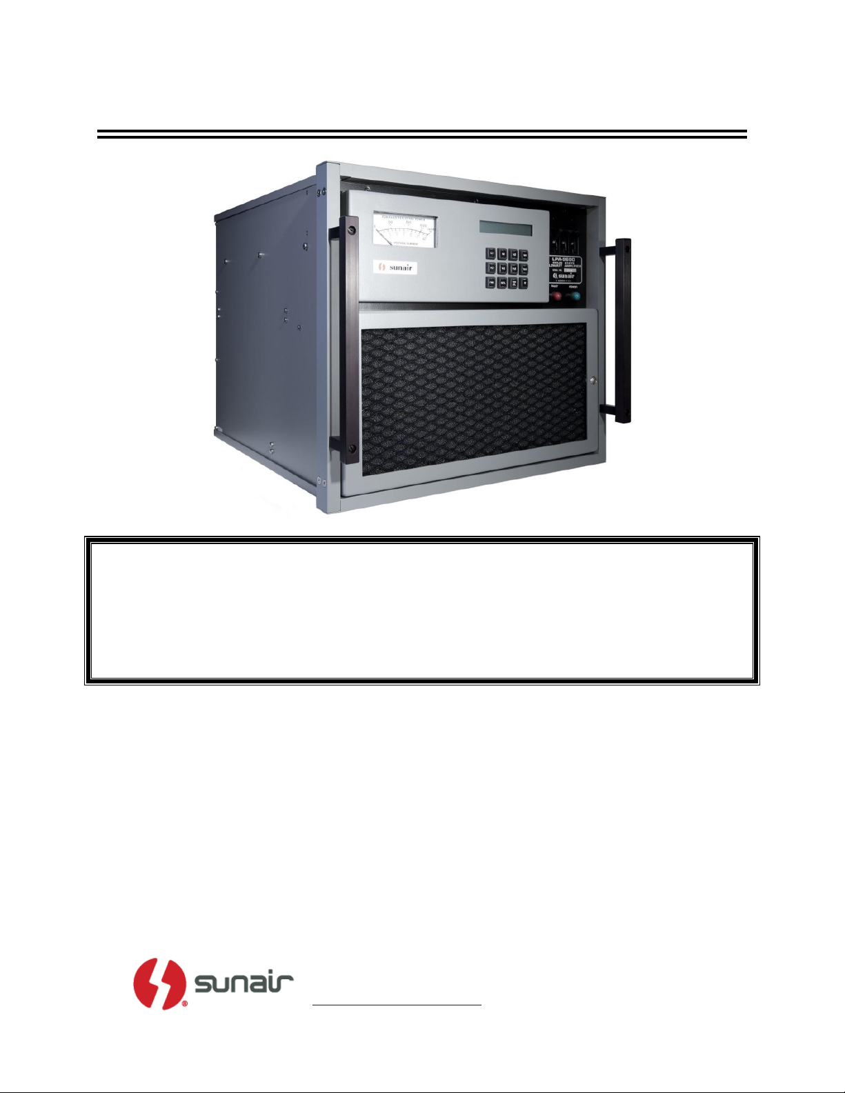
This manual describes the LPA-9600 1 kW Linear Solid State Power Amplifier and includes installation
details, operating instructions and maintenance procedures. Information in this manual applies to all
equipment configurations unless otherwise stated in the text or illustrations. The LPA-9600 is designed
specifically for operation with Sunair Transceivers and Exciters.
1.2 Purpose of Equipment
The purpose of the LPA-9600 is to amplify the low level RF output of a separate exciter to produce 1.0 kW
peak envelope power (PEP) or average power. The LPA-9600 is microprocessor controlled and operates in
the frequency range of 1.6 to 30 MHz. It is intended for a 100% unattended duty cycle for HF
communications systems networks.
1.3 General Description
1.3.1 Physical Description
Outline and mounting dimensions for the LPA-9600 are given in Figure 1.5-1. Control, power and RF
connections to the unit are made on the rear panel.
The LPA-9600 is shown in Figure 1.5-2. The amplifier is a single enclosed unit and is smaller and much
lighter, weighing only 90 lbs., than the traditional amplifiers and power supplies contained in separate units.
Top and bottom covers provide complete access for servicing. Two blowers are provided behind the front
panel filter to force cooling air throughout the amplifier.
1.3.2 Electrical Description
The LPA-9600 1KW Solid State Linear Power Amplifier is a new generation amplifier, combining solid state
RF power amplification and microprocessor technology to produce over 1000 watts of reliable HF power into
a 50 ohm load. The unit operates in the frequency range of 1.6 to 30 MHz and at a rated output of 1.5 to 1
VSWR. Four amplifier/power supply modules, each capable of producing over 300 watts, in combination
deliver a very conservative 1000 watts of peak envelope or continuous RF output power.
The LPA-9600 operates from 115 or 230 VAC (50 to 60 Hz). It is extremely rugged and withstands
temperatures up to +65°C (+149°F) while operating at a 100% duty cycle. Forced air cooling, under
microprocessor control, is utilized to maintain safe operating temperature.
The unit is capable of providing a reduced power mode (500 watts) and a bypass mode (65 or 125 watts) that
is locally keyboard selected. Also available by keyboard are status indications of power, individual amplifier
voltages and currents. The liquid crystal display (LCD) indicates the specific function selected.
Sophisticated diagnostics, status monitoring and routine housekeeping are all under microprocessor and
software control. In the event of malfunction the LPA-9600 automatically selects the next lower safe
operating level, flashes a warning light locally, and displays the cause of the malfunction on the LCD. If the
malfunction is caused by more than one failure, the operator or technician is able to obtain detailed
diagnostics by use of the keyboard.

LPA-9600
1-2 Use or disclosure of information from this document is subject to the restrictions
1.3.2.1 Expected EMP Performance
The LPA-9600 is designed with an EMP environment in mind. All control and power lines into and out of
the LPA-9600 are filtered. This filtering on the standard unit is adequate for a mild EMP. But for full EMP
hardening, the optional EMP filter, which replaces the existing filter, is required. This filter is designed per
approved EMP techniques and decouples every input and output line (except the antenna).
Although the output elements in the LPA-9600 are solid state rather than vacuum tube, they are adequately
protected from EMP damage by shielding and specially designed filtering and decoupling of all interface
lines.
1.4 Specifications
RF Output Power: 1 kW ± 1 dB PEP and average. 500W or bypass output, front panel
keyboard selected.
RF Input Power: 75W maximum.
Frequency Range: 1.6 to 30.0 MHz.
Duty Cycle: Continuous.
Type of Emission: AM, SSB, CW or any other type within the bandwidth and power
capabilities of the amplifier.
Weight: 90 lbs. (40.8 kg).
Dimensions: CM: 45.42W X 48.26D X 40.01H
Inches: 17.88W X 19D X 15.75H
Input Impedance: 50 Ohm nominal. 2.0:1 VSWR maximum.
Output Impedance: 50 Ohm unbalanced.
Load VSWR: Rated power at 2 to 1.0, reduced power up to 3 to 1, protected above 3 to
1.
Input Voltage: 115/230 VAC ±15%, single phase, 50 to 60 Hz.
Input Power: 4.5 kVA Typical (including exciter).
Intermodulation
Distortion: 36 dB or better below PEP with a standard two tone test
signal at rated power output.
Harmonic Attenuation: 73 dB or better below carrier at rated power output into a 50 Ohm load.
Spurious: 80 dB below PEP.
Band Change Time: 10 ms maximum.
Tuning Time: 0 seconds without coupler; with an Automatic Antenna Coupler, tuning time
dependent on coupler type.

LPA-9600
Use or disclosure of information from this document is subject to the restrictions 1-3
Temperature Range: Operating: -30ºC to +65ºC (-22ºF to +149ºF)
Storage: -40ºC to +85ºC (-40ºF to +185ºF)
Humidity: MIL-STD-810C, Method 507.1, Proc. III.
Altitude: 0-10,000 feet.
Vibration: MIL-STD-810C, Method 514.2, Equipment Category f, Table 514.2-VI for
wheeled vehicles, Figure 514.2-6, Curve V.
MTBF: 6,000 hours (calculated).
MTTR: 15 minutes.
Diagnostics: Microprocessor controlled with English Language Readout.
1.5 Dimensions
Figure 1.5-1 shows the dimensions for the LPA-9600 Power Amplifier.
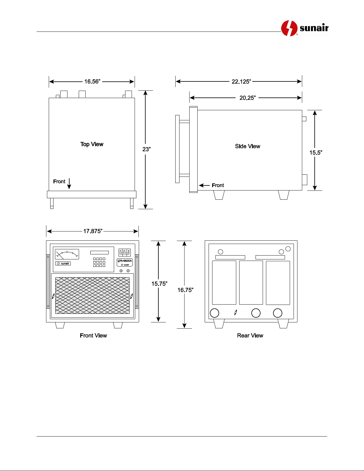
LPA-9600
1-4 Use or disclosure of information from this document is subject to the restrictions
Figure 1.5-1: LPA-9600 Outline and Mounting Dimensions

LPA-9600
Use or disclosure of information from this document is subject to the restrictions 1-5
Figure 1.5-2: LPA-9600 Front and Rear Panels

LPA-9600
1-6 Use or disclosure of information from this document is subject to the restrictions
1.6 Equipment Supplied
Table 1.6-1 lists the equipment supplied with the LPA-9600.
Table 1.6-1: LPA-9600 Equipment Supplied
Equipment
Sunair Part Number
LPA-9600, 1 KW Linear Solid State Power
Amplifier
8105000059 Gray
8105000091 Green
Power Cable Assembly (10 feet)
8066002297
Operation and Maintenance Manual
TM-8105000504
Connector Kit, consisting of:
8066000294
• 2 EA Bushing, Telescoping, .56 ID
0700550054
• 2 EA Bushing, Telescoping, .62 ID
0700550062
• 2 EA Bushing, Telescoping, .75 ID
0700550071
• 1 EA Connector, RF, UHF, PL-259
0742190005
• 1 EA Connector, RF, N UG-536B/U
0747020001
• 1 EA Connector, RF, N UG-21B/U
0754140008
• 1 EA Connector, Power, 37 Pin Round
0754320006
• 2 EA Clamp, Cable, Connector
0754570002
• 1 EA Connector, Power, 24 Pin Male
1008390011
1.7 Equipment Required, Not Supplied
Table 1.7-1 lists the equipment required, but not supplied, for the LPA-9600.
Table 1.7-1: LPA-9600 Equipment Required, Not Supplied
Equipment
Sunair Part Number
External AC Power Connector
User Supplied
Transceiver or Exciter
Consult Sunair
Coaxial Cable, RG-8A/U
0588640000
Coaxial Cable, RG-58A/U
0588130001
Antenna System, 50 Ohm Nominal
User Supplied
Transceiver to LPA-9600 Control Cable
without connectors
0579240002
Transceiver to LPA-9600 Control Cable
assembly(specify length) consisting of:
• Cable 0579240002, 9000 Series
• Mating Connector and hardware
8076004098
LPA-9600
Use or disclosure of information from this document is subject to the restrictions 1-7
1.8 Optional Equipment
Table 1.8-1 lists the optional equipment for the LPA-9600.
Table 1.8-1: LPA-9600 Optional Equipment
Equipment
Sunair Part Number
Running Spares Kit
8066900198
Service Kit (Contains PC Assembly Card
Extenders)
8066000995
Depot Spares Kit
8066900091
Field Module Kit
8066905793
CU-9150 High Speed Digital Antenna
Coupler
8120000056 Gray
8100001371 Green
LPA-9600 to CU-9150 Control Cable
8092500096
Rack Mounting Kit
8066004257 Gray
8066004290 Green
Wired Rack
8105150051 Gray
8105150093 Green
Shockmount Kit, Equipment Rack
6032090892
35 Foot Fiberglass Antenna
0715850008
KW Longwire Antenna Kit
1003090010

LPA-9600
1-8 Use or disclosure of information from this document is subject to the restrictions
THIS PAGE INTENTIONALLY LEFT BLANK

LPA-9600
Use or disclosure of information from this document is subject to the restrictions 1-1
CHAPTER II
2.0 Installation
2.1 General
Section II contains all necessary instructions for unpacking, inspection, and, if required, reshipment of the
equipment or parts. Information regarding location and mounting considerations, power requirements, ground
system hook-ups, and cabling considerations is also provided.
2.2 Unpacking and Inspection
WARNING
The LPA-9600 ships with internal packing material.
You MUST open the top cover and remove the packing
material BEFORE operating the unit.
The LPA-9600 1 kW Linear Solid State Power Amplifier is packed in a box using double wall construction. The
packing material should be removed carefully and the contents inspected for physical damage. Any claims for
shipping damage must be filed promptly with the transportation company. If it is found necessary to file such a
claim, retain all packing material.
Do not accept a shipment when there are visible signs of damage to the shipping container until a complete
inspection is made. If there is a shortage of items or evidence of damage is noted, insist on a notation to that
effect on the shipping papers before signing the receipt from the carrier. If concealed damage is discovered after
the shipment has been accepted, notify the carrier immediately in writing and await his inspection before making
any disposition of the shipment. A full report should also be forwarded to Sunair.
Be sure to include the following information for prompt service:
• Order Number
• Model and Serial Number
• Name of Transportation Agency
• Applicable Dates
Upon receipt of this information, arrangements will be made by Sunair for repair or replacement.

LPA-9600
1-2 Use or disclosure of information from this document is subject to the restrictions
2.3 Returning Equipment to Factory
The shipping container for the LPA-9600 has been carefully designed to protect the equipment during shipping.
The container and its associated packing materials should be used to reship the unit. When necessary to return
equipment to Sunair for warranty or non-warranty repair, an authorization number is required. This number can
be obtained from our Product Services Department: 954-400-5122 or 954-400-5123.
If the original shipping carton is not available, be sure to carefully pack each unit separately, using suitable
cushioning material where necessary. Very special attention should be given to providing enough packing
material around connectors and other protrusions from the equipment. Rigid cardboard should be placed at the
corners of the equipment to protect against denting. DO NOT USE POLYSTYRENE FOAM PEANUTS FOR
PACKING PROTECTION, they may allow the unit to shift while being shipped, and become damaged.
When returning equipment to Sunair for warranty or non-warranty repair, do the following:
• Obtain a Return Material Authorization number. Refer to Return Material Authorization (RMA)
Procedures at the beginning of this manual for RMA instructions.
• Prepay shipments consigned to the address provided by the Sunair Service Department
representative.
• Use indelible ink to plainly mark the following on all documents included with the shipped
items:
US Goods Returned for Repair
Value for Customs - $(Amount) – If applicable
• Mark all sides of the package as FRAGILE – ELECTRONIC EQUIPMENT
• Carefully inspect the container to be sure it is properly and securely packaged, includes all necessary
documentation, and is properly marked.
2.4 General Installation Information
Satisfactory operation of your equipment depends on the care and thoroughness taken during installation.
2.4.1 Station Layout
The LPA-9600 must be installed in a structure which provides protection from the weather. Ambient temperature
must be maintained between - 30°C (-22°F) and +65°C (144°F).
Refer to Figure 1.5-1 to see the necessary outline dimensions required for installation. Floor load is 90 pounds.
Allow free circulation of air around the cabinet, and at least six inches air space between the back of the unit and
any wall or partition. The companion transceiver may be placed on top of the LPA-9600 for voice or CW modes
of communications. For FSK or other modes requiring a full kilowatt of average power output, the transceiver
should be located on an adjacent table and have a blower kit. The transceiver may also be rack-mounted above
the LPA-9600 if blowers are provided in the top of the rack.

LPA-9600
Use or disclosure of information from this document is subject to the restrictions 1-3
2.5 Configurations
Figure 2.6-1 through Figure 2.6-3 are illustrations of various LPA-9600 configurations.
2.6 Antennas and Ground Systems
The LPA-9600 is designed to work with two types of antenna:
• Non-resonant antennas where an antenna coupler is used.
• Broadband antennas where the LPA-9600 is connected directly to the antenna.
Figure 2.6-1 through Figure 2.6-3 illustrate configurations where each of these two types of antennas are used.
2.6.1 Random Length Non-Resonant Antennas
The antenna impedance of non-resonant antennas is dependent on the operating frequency. An antenna coupler
must be used to match the antenna to the LPA-9600. Thirty-five foot whip antennas offer a good compromise
between practical height and good electrical performance at low operating frequencies. The performance of the
35-foot whip is greatly influenced by its ground system. For Base Station roof top installation, see Figure 2.6-2
for grounding details.
Another non-resonant antenna is the longwire. The two most popular length longwire antennas are 75 and 150
feet. Both of these antennas require an antenna coupler to match the antenna to the LPA-9600. Figure 2.6-4 is an
illustration of a 75-foot longwire installation. Note that the feed line from the antenna to the coupler is part of the
antenna’s length.
2.6.2 Broadband 50 Ohm Antennas
These are generally complex, expensive antennas requiring a large area for installation. Their use is usually
limited to high performance base station installations which must operate at diverse frequencies. As this class of
antenna has approximately 50 ohm output impedance over the rated band of frequencies, an antenna coupler is not
required. Some common types of broadband antenna are the Discone and Log-Periodic. Figure 2.6-1 is an
example of a system configuration utilizing a broadband antenna.

LPA-9600
1-4 Use or disclosure of information from this document is subject to the restrictions
Figure 2.6-1: LPA-9600 with Broadband Antenna

LPA-9600
Use or disclosure of information from this document is subject to the restrictions 2-5
indicted on the proprietary/confidentiality page of this document.
Figure 2.6-2: LPA-9600 with CU-9150, 35-Foot Antenna (Roof Top Installation)

LPA-9600
2-6 Use or disclosure of information from this document is subject to the restrictions
indicated on the proprietary/confidentiality page of this document.
Figure 2.6-3: LPA-9600 with CU-9150, Non-Resonant Antenna

LPA-9600
Use or disclosure of information from this document is subject to the restrictions 2-7
Figure 2.6-4: kW Long Wire Antenna Kit

LPA-9600
2-8 Use or disclosure of information from this document is subject to the restrictions
2.7 External Connections
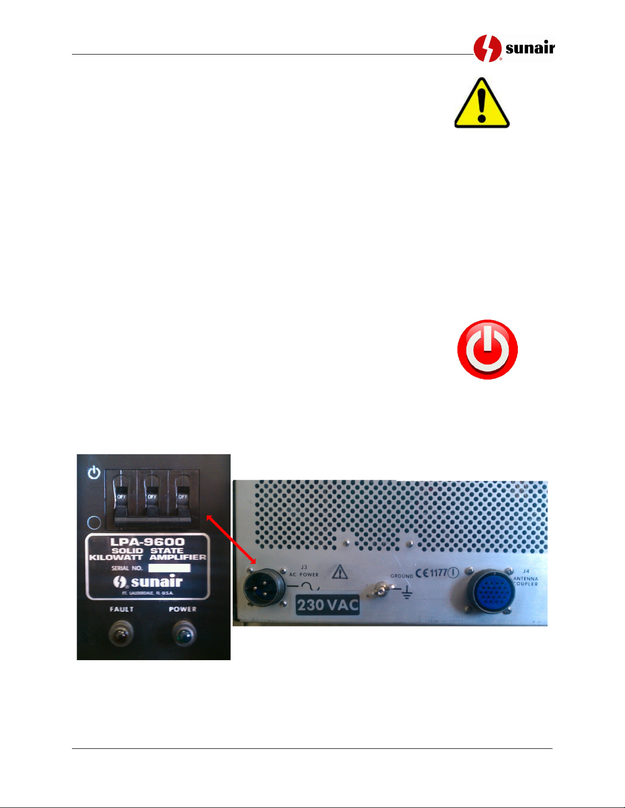
2.7.1 Primary Power Connections
The LPA-9600 requires a primary power source that can provide up to 3.5 kVA (115 or 230 VAC).
Whenever possible, the primary power source should be connected to the amplifier through a double-pole, 30
ampere capacity, manual disconnect switch (60 ampere if primary source is 115 VAC). An arrangement of
this type will insure that all power has been removed from the unit prior to entrance for servicing. Refer to
Figure 2.7-1 primary power interconnect diagram for the line voltage connection details. The Power Cable
Assembly contains three each NO. 10 AWG conductors. The green wire connects to the station primary
power ground system. The black and the white wires connect to the 115 or 230 volt power source at the
disconnect switch previously described. The standard cable as furnished is 10 feet long.
2.7.2 Transceiver Connections
Separation between the transceiver and the amplifier may be up to 150 feet. The control cable to the
transceiver is shown in Figure 2.7-2. The transceiver accessory plug, P6, is furnished with the transceiver.
The plug P5, is furnished with the LPA-9600. The control cable 0579240002 is 37 conductor, No. 20 AWG
wire, shielded and jacketed. This cable is available in lengths specified by the customer.
The RF coaxial cable is also available in lengths specified by the customer. Type RG-58A/U, P/N
0588130001 is adequate for transceiver to amplifier spacings of less than 50 feet. For distances above 50 feet,
RG-8A/U, P/N 0588640000 should be used. Connector kits are provided with the LPA-9600 and the
transceiver.
2.7.3 RF Output Connections
The amplifier’s RF output connector is also furnished in the Connector Kit. RG-8A/U coaxial cable should
be used, regardless of the distance to the antenna or antenna coupler.
Figure 2.7-1: Power Cable Assembly, P/N 8066002297

LPA-9600
Use or disclosure of information from this document is subject to the restrictions 2-9
Figure 2.7-2: 9000 Series Exciter/Transceiver to LPA-9600 Control Cable

LPA-9600
2-10 Use or disclosure of information from this document is subject to the restrictions
2.7.4 Antenna Coupler Connections
If an antenna coupler is not used, be sure the Connector Assembly P/N 8066007094 is installed on the rear of
the LPA-9600, J4.
NOTE: This connector links pin J4-T (Coupler Connect) to pin J4-G
(Ground).
When an antenna coupler is to be used, the buss wires on connector P/N 1008390011 must be removed before
cable construction is accomplished using this connector.
2.7.5 Station RF Ground System Connections
Grounding terminals are provided on the transceiver, LPA-9600 and antenna coupler for connection to the
station RF ground system. Use 1 or 2 inch wide copper strap or NO. 6 AWG wire or larger for this bonding.
Keep lead lengths to a minimum.
2.8 Preliminary Checks and Adjustments
Determine from the voltage customizing label the proper line voltage for the unit being installed. Connection
changes necessary to change voltage customizing are shown in Figure 2.8-1 and Figure 2.8-2. Be sure that
the Fan Voltage Switch, A10S1, is in the proper position.
If the LPA-9600 is received as a system with its companion transceiver/exciter, no adjustments should be
necessary. Otherwise, set the power levels as follows (see Figure 5.7-1 for component locations):
• Set transceiver/exciter frequency to 14.2000 MHz. Set transceiver/exciter MODE to CW, LPA-9600
to 1 kW. Key transceiver/exciter and adjust A3A2R32 for 1000 watts out.
• Set LPA-9600 to 500W. Set A3A2R33 for 500 watts out.
• Set transceiver/exciter to AM, LPA-9600 to 1 kW. Key transceiver/exciter and adjust A3A2R42 for
400 watts out.
• Set LPA-9600 to 500W. Adjust A3A2R43 for 200 watts out.

LPA-9600
Use or disclosure of information from this document is subject to the restrictions 2-11
Figure 2.8-1: Voltage Customizing - Circuit Breaker/Auxiliary Power Supply

LPA-9600
2-12 Use or disclosure of information from this document is subject to the restrictions
Figure 2.8-2: Voltage Customizing – RF/PS Module A4 (4 Each)
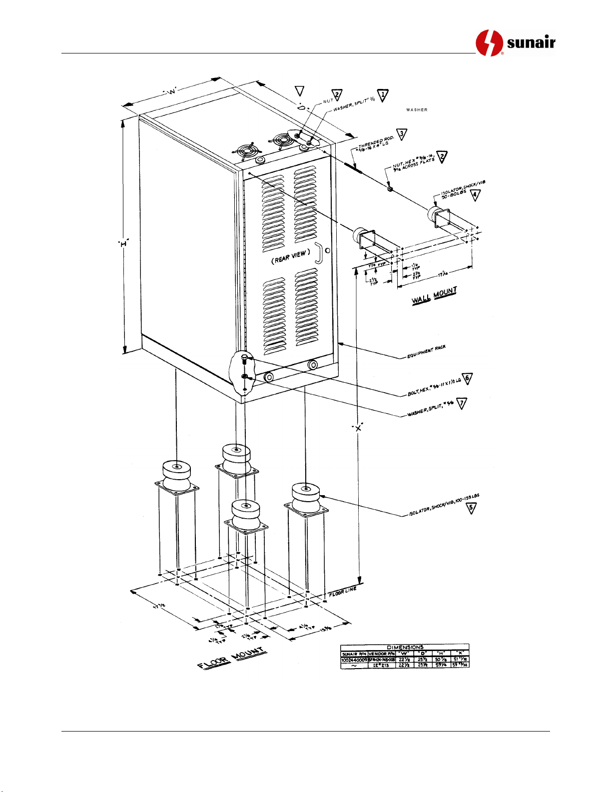
2.9 Rack Mounting Kit Option
An optional slide rack mounting kit is available to facilitate installation of the LPA-9600 in standard E.I.A.
equipment racks. See Figure 2.9-1, Figure 2.9-2, Table 2.9-1 and Table 2.9-2.

LPA-9600
Use or disclosure of information from this document is subject to the restrictions 2-13
Figure 2.9-1: Rack Mount Slide Details
Table 2.9-1: LPA-9600 Rack Mounting Kit Parts List
Sunair Part Number
Description
80660042XX
Rack Mounting Kit
50660043XX
Bracket, Rack Mounting
6032041204
Chassis Slide
0538750006
Nut, Clip 10-32
0538870001
Screw, Ornamental 10-32 x 1/2 L
1002860032
Shim, Plate LPA/PS
LPA-9600
2-14 Use or disclosure of information from this document is subject to the restrictions
Figure 2.9-2: Shockmount Equipment Rack with Outline Dimensions and Details
(Page 1 of 2)

LPA-9600
Use or disclosure of information from this document is subject to the restrictions 2-15
Figure 2.9-2: Shockmount Equipment Rack with Outline Dimensions and Details
(Page 2 of 2)

LPA-9600
2-16 Use or disclosure of information from this document is subject to the restrictions
Table 2.9-2: LPA-9600 Shockmount Kit Equipment Rack Parts List, P/N 6032090892
Sunair Part Number
Description
Qty
0501650008
Washer, Split 3/8
2
0501700005
Nut, Hex 3/8-16 X 9/16 AF
4
0542880644
Rod, Thd 3/8-16 X 4 Lg
2
0841810001
Isolator, Shock/Vib. 50-80 Lbs
2
1001280016
Isolator, Shock/Vib. 100-155 Lbs
4
1001290003
Bolt, Hex 5/8-11, 1½1/2 Lg
4
1001300009
Washer, Split 5/8
4
1002980011
Installation Instructions
1

LPA-9600
Use or disclosure of information from this document is subject to the restrictions 2-1
CHAPTER III
3.0 Operation
3.1 General
This section provides information and instructions required for operation of a transceiver, the LPA-9600 1
kW Linear Solid State Power Amplifier and an automatic antenna coupler. Refer to the transceiver and the
coupler Operation and Maintenance Manuals for detailed information regarding operation of these units.
3.2 Function and Location of Controls and Indicators
Figure 3.2-1 shows the location of the LPA-9600 front panel controls and indicators. Their functions are listed
in Table 3.2-1.
Figure 3.2-1: LPA-9600 Controls and Indicators

LPA-9600
2-2 Use or disclosure of information from this document is subject to the restrictions
Table 3.2-1: Front Panel Controls and Indicators
Control or Indicator
Function
Meter, A2M1
Displays the following:
• 0 - 1400: Forward Power in watts
• 0 - 140: Reflected Power in watts
• 0 - 60V: Selected PA’s voltage
• 0 - 18A: Selected PA’s current
LCD Assembly, A2A2
This Liquid Crystal Display (LCD) displays all systems messages and
conditions.
Circuit Breaker, A8CB1
Applies primary power to the LPA-9600.
FAULT Lamp, A8DS2
A red fault lamp which, when flashing, indicates a fault in the LPA-9600.
A steady fault lamp indicates a fault external to the LPA-9600.
POWER Lamp, A8DS1
A green lamp which indicates that primary power has been applied to the
LPA-9600.
Keyboard, A2A1S1
The keyboard lets the operator/technician check individual voltage,
current and power levels. The keyboard also provides the
operator/technician with the ability to select desired power operating
levels and to read failure indications.
• Ic = Current Collector
• Vc = Voltage Collector
• PA = Power Amplifier
Ic1
When pressed, displays power supply current of PA #1 on meter.
Ic2
When pressed, displays power supply current of PA #2 on meter.
Ic3
When pressed, displays power supply current of PA #3 on meter.
Ic4
When pressed, displays power supply current of PA #4 on meter.
Vc1
When pressed, displays power supply voltage of PA #1 on meter.
Vc2
When pressed, displays power supply voltage of PA #2 on meter.
Vc3
When pressed, displays power supply voltage of PA #3 on meter.
Vc4
When pressed, displays power supply voltage of PA #4 on meter.
FWD
When pressed, displays forward output power (in watts) on meter.
REFL
When pressed, displays reflected output power (in watts) on meter.
PWR LVL
When pressed, changes output power level reading on LCD from 1 kW to
500 watts to bypass.
*
When more than one fault occurs, the LCD will read Fault: MULTIPLE..
PRESS *. Press this key to display each fault message one at a time
until all faults detected have had messages displayed.

LPA-9600
Use or disclosure of information from this document is subject to the restrictions 2-3
3.3 Operating the LPA-9600
WARNING
The LPA-9600 ships with internal packing material.
You MUST open the top cover and remove the packing
material BEFORE operating the unit.
3.3.1 Operation with a 9000 Series Exciter/Transceiver
Insure that the transceiver/exciter and the LPA-9600 are installed properly by referring to Section II of this
manual and in the radio manual. If an antenna coupler is being used, insure its proper installation as well.
1. Apply power to the transceiver/exciter and LPA-9600. The LPA-9600 POWER lamp will light and
the LCD will display a system message.
• Without an automatic antenna coupler: kW SYSTEM OPERATIONAL, METER: FWD, PWR
LVL: 1 kW. (Instead of PWR LVL: 1 kW, it may display Bypass if it’s not programmed in the
exciter). Then kW SYSTEM OPERATIONAL appears and the system is ready to operate. If
instead the FAULT lamp on the LPA-9600 flashes, this indicates a fault in the LPA-9600. Reset
the LPA-9600 by turning the transceiver/exciter off, wait 30 seconds, then turn back on; or at the
LPA-9600 turn circuit breaker OFF then ON; or using the PWR LVL key on the keyboard, reset
the LPA-9600. If FAULT does not clear, refer to Section V of this manual.
• With a CU-9150 antenna coupler: FAULT: COUPLER UNTUNED, METER: FWD, PWR LVL:
1 kW. If there is a coupler fault, the LPA-9600 FAULT lamp will burn steadily. Follow steps 2
through 6 below.
2. Select operating frequency on transceiver/exciter.
3. If a coupler is present, press the CPLR TUNE button on the 9000 Series front panel.
4. The LCD will display system messages: COUPLER TUNING, COUPLER TUNED, and kW SYSTEM
OPERATIONAL. After tuning is complete, (maximum 2 seconds), the system is ready for operation.
5. If after a tune attempt, the FAULT lamp on the LPA-9600 burns steadily, this indicates a fault in the
coupler, antenna, or feedline. Attempt retuning. If the fault does not clear, refer to Section V of this
manual and the 9000 Series or coupler manual.
6. If the FAULT lamp on LPA-9600 flashes, this indicates a fault in the LPA-9600. Reset the LPA-
9600. If the fault does not clear, refer to Section V of this manual.
NOTE: If an antenna coupler is not used, tuning is not required when the
operating frequency of the transceiver/exciter is changed. With an
antenna coupler, coupler tuning is required with each frequency
change.

LPA-9600
2-4 Use or disclosure of information from this document is subject to the restrictions
THIS PAGE INTENTIONALLY LEFT BLANK

LPA-9600
Use or disclosure of information from this document is subject to the restrictions 3-1
CHAPTER IV
4.0 Theory of Operation
4.1 General
See Figure 4.11-1 and Figure 5.8-1.
The LPA-9600 is an all-solid-state, self-contained, one kilowatt linear power amplifier designed for use with
9000 Series transceivers or exciters. The unit is complete in one package and includes RF amplifier modules,
power supplies, combining networks, harmonic filters and microprocessor control circuitry. Built-in
diagnostics monitor the functional operation of the unit and report malfunctions in English language on a
front panel liquid crystal alphanumeric display. In addition to reporting malfunctions, the microprocessor
reconfigures the amplifier to a safe operating power level, or shuts it down completely, providing exciter only
operation.
The RF circuitry consists of an input power splitter, four broadband RF power amplifier modules, an output
power combiner, and a harmonic low pass filter. The input power splitter divides the exciter power equally
among the four RF modules. Each RF amplifier module consists of two conservatively rated power
amplifiers combined to provide over 300 watts power output capability. The output from the four RF
amplifier modules is combined in the output power combiner, providing over 1200 watts output capability in
one feedline. The harmonic low pass filter attenuates the harmonic output of the amplifiers by at least 75 dB.
The filter is split into 8 bands, each a maximum of one-half octave frequency span (1.5 x frequency),
automatically selected by the exciter and buffered by the microprocessor circuitry, so that no tuning is
required.
Each power amplifier module consists of an RF module, a power supply, and an RF module control assembly.
The power supplies are high-efficiency switching regulators, with built-in current foldback and overvoltage
protection. The RF module control assembly provides microprocessor-controlled AC power input to the
power supplies, and regulated bias voltage to the dual amplifier, ensuring linearity.
4.2 Control Panel Module A2
See Figure 5.8-2.
The Control Panel Module is a plug-in panel arrangement on the front of the LPA-9600 which contains the
meter, the LCD Assembly, and the 3 x 4 keyboard. The LCD Assembly A2A1 is used to display the power
level selected, the diagnostic information, and the function selected to be displayed on the meter. The 3 x 4
keyboard is used to select the meter display functions. The PC Assembly Control Panel A2A2 provides the
interconnections which permit the keyboard to close the proper row to the proper column when a key is
pressed and pass the information on to the Computer Mother Board A3A1. The PWR LVL key is used to
select the desired operating power level of the LPA-9600. The * key is used to scroll through multiple fault
indications. The meter is used to display any of the four collector currents, four collector voltages, and either
forward or reflected power.

LPA-9600
3-2 Use or disclosure of information from this document is subject to the restrictions
4.3 Computer Assembly A3
4.3.1 PC Assembly Computer Mother Board A3A1
See Figure 5.8-3.
The Computer Mother Board acts as a back plane to interconnect the Peripheral Board A3A2 to the
Microprocessor Board A3A3 and to interconnect these two boards to the balance of the LPA-9600. The
Microprocessor Board plugs into A3A1J6 and A3A1J7. The Peripheral Board plugs into A3A1J8 and
A3A1J9. Connector A3A1J1 provides routing for the signals to and from the power amplifier assemblies.
Connector A3A1J2 interfaces to the Filter Module A5. Connector A3A1J3 connects to the Control Panel
Module A2. Connector A3A1J4 interfaces with the transceiver/exciter and the antenna coupler. Connector
A3A1J5 interfaces with the front panel of the LPA-9600 by transferring control signals to the front panel
lights, the bypass relay, and overtemperature fan.
4.3.2 Peripheral Board A3A2
See Figure 4.11-2 and Figure 5.8-4.
4.3.2.1 General
The Peripheral Board A3A2 contains much of the analog circuitry used to monitor and control the LPA-9600.
Many fault indicators and detectors are located on this board. These circuits are designed to inform
Microprocessor A3A3U1 when a fault has occurred in the electronic operation of the LPA-9600. Also
provided are circuits which interface it with a CU-9150 Digital 1000W Coupler.
The Peripheral Board is responsible for the following functions required for proper operation of the LPA9600:
• The signal BYPASS which causes the LPA-9600 to be bypassed in the event of a fault which in turn
inhibits it from producing its power output.
• The signals READY REMOTE , kW DETECT , FAULT REMOTE , kW POWER DETECT 1, and
kW POWER DETECT 2 operate circuits in the 9000 Series Exciter/Transceiver.
• The signal used to drive the fault lamp on the front panel of the LPA-9600.
• The signal +28 VDC TUNE ENABLE which instructs the transceiver that a CU-9150 antenna coupler
is attached and is tuning.
The Peripheral Board contains the multiplexer circuits which permit ten of the twelve front panel keys on the
keyboard to select meter functions. Contained also is a DC to DC converter to provide contrast adjustment
for the front panel LCD Assembly. Similarly, a DC to AC inverter is provided which drives the EL
(electroluminescent lamp) backlight for night time viewing of the LCD Assembly. Also provided is the
ALC/ACC Control Circuit which monitors the forward and reflected power. This circuit is responsible for
selecting and producing the proper level of ALC or ACC needed to control the 9000 Series equipment
attached to the LPA-9600.

LPA-9600
Use or disclosure of information from this document is subject to the restrictions 3-3
4.3.2.2 Temperature Sense Comparators U1, U2
The purpose of the Temperature Sense Comparators is to detect when the temperature on any of the four
heatsinks on the four individual power amplifiers has reached either of two thresholds. When the temperature
on any power amplifier heatsink reaches between 75°C and 85°C (167°F and 185°F), Microprocessor
A3A3U1 causes the fans to operate at a higher speed. If the temperature continues to increase and reaches
between 100°C to 120°C (212°F to 248°F), A3A3U1 shuts down the overheating power amplifier.
4.3.2.3 Overtemperature Buffer U3
The purpose of the Overtemperature Buffer U3 is to provide a means by which Microprocessor A3A3U1 can
monitor the temperature of power amplifier assemblies 1, 2, and 3. U3 also acts as a position from which
A3A3U1 can monitor a signal called FILTER MODULE FAULT. This signal originates in the Filter Fault
Detector U9C, U20A. If this signal is high, A3A3U1 will cause an indication on the LCD Assembly pointing
out the faulty filter module. In addition, A3A3U1 will force the LPA-9600 to BYPASS operation to protect
the filter module from damage.
4.3.2.4 Gain Fault Comparators U12
The Gain Fault Comparators are a series of four detector circuits used to monitor the power gain of the four
individual power amplifier assemblies. The input power to a particular power amplifier assembly is
compared to its output power. If the power amplifier is not producing the required amount of power,
Microprocessor A3A3U1 is alerted.
4.3.2.5 Gain Fault Buffer U7
The Gain Fault Buffer is the device by which Microprocessor A3A3U1 monitors the status of the gain of the
four power amplifier assemblies. When any of the GAIN FAULT signals go high, A3A3U1 will cause a gain
fault message to be displayed on the LCD Assembly A2A2. At the same time A3A3U1 will shut down the
defective power amplifier reducing the output power from 1000 watts to 500 watts in the LPA-9600. U7 is
also used by A3A3U1 to monitor the temperature information from power amplifier number 4 received from
the temperature sense comparators. The signal VSWR FAULT is also monitored by A3A3U1 thru U7. If this
signal goes high, A3A3U1 will reduce the power produced by the LPA-9600 from 1000 watts to 500 watts. If
VSWR FAULT is still high, A3A3U1 will place LPA-9600 in BYPASS, protecting it from the excessive
VSWR.
4.3.2.6 VC Monitor Comparators U11
The purpose of the VC Monitor Comparators comprising U11 is to monitor the individual+48V power
supplies that are mounted in each of the four power amplifier assemblies. When the voltage in a power
supply falls below +42.3 volts, the output of U11 goes high. Microprocessor A3A3U1 will sense this and
remove the defective power supply from operation.
4.3.2.7 Voltage Monitor Comparators U13
The purpose of the Voltage Monitor Comparators comprising U13 is to monitor the +28VDC and +5VDC
utilized by the logic control circuitry in the LPA-9600. Microprocessor A3A3U1 monitors the four outputs of
U13 to determine if the voltages are too high or too low.

LPA-9600
3-4 Use or disclosure of information from this document is subject to the restrictions
4.3.2.8 VC Monitor/Voltage Monitor Buffer U19
U19 is used by Microprocessor A3A3U1 to determine if any of the four +48V power supplies is producing a
voltage that is too low. U19 is also used to determine if the +28V logic control voltage is too low or if the +5
V logic control voltage is too high or too low. A3A3U1 periodically samples the inputs of U19. If any of
these inputs are high, A3A3U1 takes appropriate action and alerts the operator to the condition.
4.3.2.9 Collector Voltage Meter Conditioning Circuit U14
U14 functions as four distinct identical stages. U14A conditions the +48V from PA #1 for display on the
meter, U14C conditions the +48V for PA #2, U14B conditions the +48V for the PA #3, and U14D conditions
the +48V for PA #4. These circuits are voltage follower circuits which function identically. For example:
For PA #1, +48V is applied to U14A through a resistor divider. The resistor divider reduces the +48V to
+3V, which when applied through a 33.2 k ohm resistor and U17, the 16 Channel Multiplexer (approximately
470 ohms resistance), supplies approximately 80 µA to the meter (3.7 k ohms resistance) causing a +48V
indication. (Full scale on the meter is 100 µA.)
4.3.2.10 Collector Current Meter Conditioning Circuit U16
The Collector Current Meter Conditioning Circuit performs a function similar to that performed by the
Collector Voltage Meter Conditioning Circuit U14. U16 is divided into four sections, A thru D, and acts as a
unity gain inverting amplifier which inverts a minus voltage to plus voltage for indication on the meter. Each
one is capable of conditioning the voltage which is equivalent to the collector current being drawn by each
power amplifier assembly and producing a proportionate current source to the meter to deflect it the proper
amount. Full scale deflection of the meter is equivalent to 18 amps. If a power amplifier is drawing a current
of 9 amps, the meter deflection would indicate a half-scale deflection resulting from a 50 µA current source
produced by the concerned section of U16.
4.3.2.11 16 Channel Multiplexer U17
The purpose of the 16 Channel Multiplexer is to provide a means by which different current sources can be
applied to the front panel meter as they are selected by the keyboard. Microprocessor A3A3U1 provides
binary input selection which enables U17 to select the proper analog gate circuit output to be supplied to the
meter.
4.3.2.12 Multiplexer Switch Selector Latch U18
The purpose of the Multiplexer Switch Selector Latch is to provide a means by which Microprocessor
A3A3U1 can select the proper meter information to be sent to the front panel meter to be displayed. U18
provides the binary inputs to U17 to cause U17 to select the proper keyboard selected current source to be
supplied to the meter.
4.3.2.13 Overcurrent Detectors U15
The Overcurrent Detectors are comprised of four identical circuits U15 A thru D. U15A monitors the current
in PA #1, U15B monitors PA #2, U15C monitors PA #3, and U15D monitors PA #4. The detectors are set to
detect a condition of 17.5 amps in the four power amplifier assemblies respectively. If a power amplifier is
drawing too much current, then Microprocessor A3A3U1 is alerted to the overcurrent condition by U15.
Once the condition is verified, then A3A3U1 removes that amplifier from operation, reducing the output of
the LPA-9600 from 1000 to 500 watts.

LPA-9600
Use or disclosure of information from this document is subject to the restrictions 3-5
4.3.2.14 LCD Enable Inverter U6E
A signal called LCD E is produced on the Microprocessor Board A3A3 and needs to be inverted before it
can be used by the LCD Assembly A2A2 as an enable. U6E inverts the signal to a signal called E and sends
it to the LCD Assembly where it permits the LCD to read or write information from or to Address/Data Bus
BAD0 through BAD7.
4.3.2.15 VSWR Fault Detector U9B
The purpose of the VSWR Fault Detector is to alert Microprocessor A3A3U1 that a VSWR fault is occurring,
indicating that action is required. U9B may be adjusted to trip on VSWR faults of 2:1 or 3:1 using
potentiometer A3A2R56. U9B compares the ratio of FWD PWR to REFD PWR. When REFD PWR
exceeds the threshold established by R56, the output of U9B goes high alerting A3A3U1 of the excessive
VSWR.
4.3.2.16 Filter Fault Detector U9C, U20A
The purpose of the Filter Fault Detector is to warn Microprocessor A3A3U1 when one of the filters of the
eight available is malfunctioning in such a way that power is being sent into the filter assembly but is not
exiting from it. U20A monitors the forward power leaving the LPA-9600. U9C compares the power entering
the filter modules from the power amplifiers with the power leaving the LPA-9600. A3A3U1 monitors the
output of U9C and if it goes high for longer than 50 ms, then A3A3U1 causes the LPA-9600 to go to
BYPASS by shutting down the power amplifier assemblies, preventing them from damaging the filter
module.
4.3.2.17 RF Present Detector Q4
The RF Present Detector is connected to the signal P OUT MONITOR as is U9C of the Filter Fault Detector
circuit. If power is present on P OUT MONITOR, Q4 will be turned on, producing a low on U8, the Coupler
Interface Buffer. When Microprocessor A3A3U1 detects the low, then it knows through its software that the
power amplifiers are producing power. Since certain faults can only be legitimate faults in the presence of
RF, A3A3U1 will monitor these only if RF is present.
4.3.2.18 Forward Power Meter Conditioning Circuit U10B, U23A AND Q13
U23A and Q13 is a peak detector circuit used to drive U10B. U10B is configured as a voltage follower. Its
purpose is to buffer the forward power information that the Peripheral Board receives. U10B produces a
voltage which is sent to two places. Through potentiometer A3A2R61 this information is called FWD PWR
LOCAL and goes to A3A2U17, the 16 Channel Multiplexer. (R61 is used to adjust the full scale level of
FWD PWR LOCAL on the front panel meter of LPA-9600.) The other signal produced is FWD PWR
REMOTE which is transferred to the meter on the 9000 Series Exciter/Transceiver display. The approximate
power level of the LPA-9600 is read on this meter.
4.3.2.19 Reflected Power Meter Conditioning Circuit U10A, U23B AND Q14
U23B and Q14 is a peak detector circuit used to drive U10A. The function of the Reflected Power Meter
Conditioning Circuit is identical to the function of U10B. A3A2R59 is used to adjust the full scale deflection
of the reflected power information on the front panel meter of the LPA-9600.

LPA-9600
3-6 Use or disclosure of information from this document is subject to the restrictions
4.3.2.20 Reflected Fault Detector U9D
The purpose of the Reflected Fault Detector is to warn Microprocessor A3A3U1 when a severe reflected fault
condition is occurring in the LPA-9600. If the reflected power level reaches and exceeds 200 watts, U9D
goes high. A3A3U1 checks the reflected fault condition indicated by the Reflected Fault Detector to insure
that it actually exists, and if so, immediately places the LPA-9600 in BYPASS.
4.3.2.21 ALC/ACC Control Circuit U10C, U10D, U20A, B and C, Q3 and Q12
The purpose of the ALC/ACC Control Circuit is to provide ACC feedback to the transceiver when operating
in AM, and to provide ALC feedback when operating in SSB or CW. The ALC/ACC Control Circuit
monitors the summation of forward and reflected power and either increases or decreases the feedback to the
transceiver, enabling the transceiver to provide the LPA-9600 with the correct power output level.
The ALC/ACC Control Circuit functions in one of two modes. It functions either as a 1000 watt or as a 500
watt ALC/ACC circuit. The signal, 1 kW ALC/ACC , is received from the Microprocessor Board A3A3. If
this signal is a low it means that the Microprocessor Board wishes to operate in a 1000 watt mode. This low
turns on transistors Q10 and Q11 shorting out potentiometers A3A2R33 and R43. With R33 and R43
shorted, A3A2R32 and R42 would be used to adjust the ALC and ACC control levels. If 1 kW ALC/ACC is
a high indicating operation at 500 watts, this high turns off Q10 and Q11. R33 and R43 now become part of
the effect controlling the ALC and ACC voltage.
U10C is used as a buffer to amplify the reflected power. A3A2R28 is used to adjust the output of U10C.
Forward power and reflected power are summed and fed to R32 and R42 where all four potentiometers can
affect the relative level. U10D amplifies the level adjusted by R42, or R42 and R43, and drives Q3. If the
output of U10D decreases, the output of Q3 will decrease, reducing the ACC to the transceiver which
increases the RF power supplied to the LPA-9600 to compensate. U20B and U20C amplify the level adjusted
by R32 or R32 and R33 to drive Q12. If the output of U20C decreases, the output of Q12 decreases, reducing
the ALC voltage to the 9000 Series Exciter/Transceiver which increases the RF power supplied to LPA-9600
to compensate.
4.3.2.22 DC to DC Converter U21
The purpose of U21 is to provide the LCD Assembly A2A2 with a negative voltage which can be used to vary
the display contrast and intensity. +5VDC is converted to -5VDC by U21 and applied to potentiometer
A3A2R164. R164 is the adjustment for the display contrast and intensity.
4.3.2.23 DC to AC Converter U22
The purpose of U22 is to provide an AC signal to the electroluminescent lamp which backlights the LCD
Assembly A2A2. U22 accepts a +5VDC input and produces approximately 90VAC out which excites the
electroluminescent backlight, permitting night viewing of the LCD display.

LPA-9600
Use or disclosure of information from this document is subject to the restrictions 3-7
4.3.2.24 Coupler Control Circuits
4.3.2.24.1 General
The coupler control circuits employed in the LPA-9600 to permit interfacing with the CU-9150 are all located
on the Peripheral Board A3A2. The signals interfacing the CU-9150 to the LPA-9600 include: +28 VOLT
TUNE ENABLE, READY , FAULT , and COUPLER PRESENT. These signals are inputs to the LPA-9600
from the CU-9150. Several signals exit the LPA-9600 for use in the 9000 Series equipment. These are:
READY REMOTE , kW DETECT FAULT REMOTE , kW POWER DETECT 1 and kW POWER DETECT
2.
The LPA-9600 is notified that the CU-9150 is ready to tune when the LPA-9600 receives the signal +28
VOLT TUNE ENABLE. When the LPA-9600 detects this signal, it immediately selects BYPASS operation so
that the power being sent through the LPA-9600 to the CU-9150 is the power from the transceiver. The LPA-
9600 monitors signals, READY , and FAULT from the CU-9150. These signals indicate the status of the
CU-9150. The LPA-9600 utilizes these signals in an algorithm which produces the signals sent to the 9000
Series equipment to display the condition of the CU-9150 on their front panel displays.
4.3.2.24.2 Coupler Input Detectors U6A-D, U9A
The purpose of the Coupler Input Detectors is to buffer signals that originate in the CU-9150. These signals
are: +28 VOLT TUNE, ENABLE, READY , COUPLER PRESENT, and FAULT. Microprocessor A3A3U1
monitors these signals through U8, Coupler Interface Buffer. The +28 VOLT TUNE ENABLE arrives at U9A
as a high anytime the CU-9150 wishes to tune. The signal called READY when low, indicates to the LPA-
9600 at the end of the tune cycle that the CU-9150 has tuned properly. COUPLER PRESENT is used by
A3A3U1 to detect if a CU-9150 coupler is attached. FAULT when low, indicates to the LPA-9600 at the end
of the tune cycle that the CU-9150 has failed to tune properly.
4.3.2.24.3 Coupler Interface Buffer U8
The Coupler Interface Buffer is used by Microprocessor A3A3U1 to monitor the signals from the coupler
Input Detectors. U8 also monitors a signal called RF PRESENT which originates in the RF Present
Detector Q4. When RF PRESENT is low, this indicates to A3A3U1 that RF is present in the LPA-9600, and
that certain fault conditions can be monitored or detected. If the signal is high, meaning RF is not present,
A3A3U1 will ignore those fault indications. Another input to U8 is a signal called +28V TOO HIGH. If this
signal is high, it is an indication to Microprocessor A3A3U1 that the +28V is out of tolerance on the high
side.
4.3.2.24.4 Output Latch U4
Latch U4 outputs the signals produced by microprocessor A3A3U1 to activate the display messages on the
9000 Series equipment front panels and the FAULT light on the front panel of the LPA-9600. The output
signals are READY, kW DETECT, FAULT, kW POWER DETECT 1, kW POWER DETECT 2 and BYPASS.
The signal BYPASS is produced by A3A3U1 when it wishes the LPA-9600 to operate in BYPASS. This
command is issued both when A3A3U1 detects fault conditions within its operation which warrant going to
BYPASS, and when the CU-9150 is tuning.

LPA-9600
3-8 Use or disclosure of information from this document is subject to the restrictions
4.3.2.24.5 Lamp Driver/Relay Driver Circuit U5G, Q1, Q5, Q6
The purpose of the Lamp Driver/Relay Driver Circuit is to provide drive capability to the signals exiting
Latch U4 to the 9000 Series equipment and to control the Bypass relay. Transistors Q1, Q5 and Q6 control
READY REMOTE , kW DETECT , and FAULT REMOTE respectively. FAULT OUT LOCAL is also
controlled by Q6. U5G receives a high anytime Microprocessor A3A3U1 wishes to operate the LPA-9600 in
BYPASS. This causes the Bypass relay K18 in the A5 Filter Module to energize.
4.3.2.25 BITE BITS
The LPA-9600 is capable of self-checking certain elements of its circuit operation. Microprocessor A3A3U1
controls these BITE BITS, monitors them for circuits not operating properly and takes action accordingly.
4.3.3 Microprocessor Board A3A3
4.3.3.1 General
See Figure 4.11-3 and Figure 5.8-5.
The Microprocessor Board A3A3 produces three major functions in the LPA-9600. The first function is the
interfacing of the Keyboard to the meter. The second function is the driving of the LCD Display providing it
with intelligent information. The third function is the controlling of the diagnostic feature, in which all major
functions within the LPA-9600 are monitored both to provide failure information and to trigger corrective
action if a failure occurs.
Specific to the three major functions, the Microprocessor Board A3A3 is responsible for the following
activities of the LPA-9600:
• Monitors overcurrent signals and reflected fault signals from the Peripheral Board A3A2.
• Produces drive dump commands to control the Power Amplifier Assemblies A4A3 (four each).
• Monitors band information from the 9000 Series equipment so that it can produce the controlling
signals for the Filter Module Assembly A5 to select the proper Band Filter (1 through 8).
• Produces buffered address/data AD0 thru AD7 lines to the Peripheral Board and the LCD Assembly
A2A2.
• Produces signals A0 and A1 for the LCD Assembly to indicate to the LCD Assembly whether the
information it has received from the Microprocessor Board is a command or a data word.
• Produces chip selects which are used to enable various bus driven components on the Peripheral
Board.
• Produces signals which drive the power supply relays providing +48 VDC to the Power Amplifier
assemblies (four each).

LPA-9600
Use or disclosure of information from this document is subject to the restrictions 3-9
4.3.3.2 Microprocessor U1
The Microprocessor U1 controls the functions of Microprocessor Board A3A3. U1 contains three major
busses. The first bus is AD0 thru AD7, a multiplexed address/data bus containing either data or address
information. The second bus is A8 thru A15 and always contains address information. The third bus is the
control/status bus which contains signals RD , WR , IO/ M , and ALE.
When U1 wishes to obtain an instruction from EPROM U9 it produces an address on AD0 thru AD7. U1
then produces an ALE signal which latches that address into Address Latch U8 which forwards it to U9.
Once the address is directed to U9, U1 then produces RD to U9 and U9 responds by giving the instruction
stored at that address onto the AD0 thru AD7 line. U1 reads the instruction, then acts upon it.
When U1 requires a Device Selection mechanism to communicate with its input or output ports, it produces
the address on the A8 thru A15 address lines causing that port device to become enabled. When the device is
enabled, it can either read information from or write information to U1 on the AD0 thru AD7 lines.
The signals present on the control/status bus are used by U1 to transfer information. RD is used by U1
when it wishes to obtain (read) information from a device on the AD0 through AD7 lines. WR is used by
U1 when it wishes to give (write) information to a device on the AD0 thru AD7 lines. IO/ M is used by U1 to
discriminate between IO and Memory operations. If U1 is reading from or writing to memory, the IO/ M line
is low. If U1 is reading from or writing to IO the IO/ M line is high. ALE (address latch enable) is pulsed
high when U1 wishes to write an address from AD0 thru AD7 lines into the Address Latch U8 to select an
instruction from EPROM U9. When data is present on the AD0 thru AD7 lines, ALE is low.
4.3.3.3 Address Latch U8
When Microprocessor U1 produces an address on AD0 thru AD7, it also produces an ALE signal which
latches the address into U8. U8 provides continuous address information A0 thru A7 for the EPROM U9 by
sorting out the address from the data information on the AD0 thru AD7 bus. U8 also provides A0 and A1 to
drive the LCD address buffer U19.
4.3.3.4 EPROM U9
The EPROM U9 is the storage device where Microprocessor U1’s programming code is stored. When U1
wishes to fetch an instruction from U9, it will produce the upper order address of the instruction it wishes to
read on lines A8 thru A15, and the lower order address of the instruction it wishes to read on lines AD0 thru
AD7. The lower order address on AD0 thru AD7 is connected to address latch U8. When the address
information at U8 is correct and present, U1 will issue an ALE signal to latch that information into U8,
causing the output of U8, A0 thru A7, to contain the lower order address information of the instruction which
U1 wishes to fetch from U9. At the same time, U1 also causes Memory Device Selector U6A, U7, U21A, to
issue a signal called EPROM to enable U9. After a short delay, U1 will issue a RD signal to U9 causing
U9 to deposit on its output lines, AD0 thru AD7, the instruction that was stored at the address selected. When
U1 causes the RD signal to make a low to high transition, it will fetch into itself the instruction on AD0 thru
AD7 it has selected to act upon.

LPA-9600
3-10 Use or disclosure of information from this document is subject to the restrictions
4.3.3.5 Power Clear Circuit U2C, U4A, U4B
The Power Clear Circuit is necessary to initialize Microprocessor U1 when power is first applied to the LPA-
9600. The circuit provides a low on pin 36 of U1 for a time after the voltage is applied to the LPA-9600.
This holds U1 reset until transient conditions have passed. At that point, U1 is permitted to run because the
Power Clear Circuit transfers U1 pin 36 to a high.
4.3.3.6 Crystal Oscillator U34
U34 provides a reference frequency of 6.144 MHz to Microprocessor U1. All activities of U1 occur at rates
dependent on the output of U34.
4.3.3.7 Memory Device Selector U6A, U7, U21A
When U7A or U7B produce a low output they are doing so as a result of the addresses being selected properly
by Microprocessor U1 on their inputs from bus A8 thru A15. The low output enables a particular memory
device, either EPROM U9, RAM U13 or the LCD Assembly, to allow Microprocessor U1 to read from or
write to that device.
4.3.3.8 Divide by 2 Circuit U24B
U24B is a flip-flop which receives the clock output of Microprocessor U1. The clock frequency is 3.072
MHz on input pin 11 of the flip-flop. U24B divides its input and produces an output frequency of 1.536 MHz
on pin 9 to the timer portion of RAM-IO-TIMER U13.
4.3.3.9 RAM-IO-TIMER U13
U13 contains a RAM (Random Access Memory), three IO ports (has input or output capabilities), and a
TIMER which is driven by U24B.
The RAM is used by Microprocessor U1 as a temporary storage facility for information that needs to be
stored for future access or which is being acted upon in real time. The IO Ports (Input/Output Ports A, B, C)
are all selected by U1 for output operation. Port A (PA0-PA7) provides the BAND 1 thru BAND 8
information for driving the proper relay in the Filter Module A5. Port B (PB0-PB7) outputs the latch signals
which drive the power supply relays providing the power amplifier assemblies with +48 VDC. Also output
are Drive Enable which disables or enables the PA assemblies’ drive capability, Overtemp Command to
increase the speed of the blower fans 1 kW ALC/ACC to tell U1 whether to operate the LPA-9600 at 1000 or
500 watts, and the Bite Bit 2 which allows U1 to self-test various ports on the Microprocessor Board. Port C
(PC0-PC5) outputs sequential lows on Rows 1-3 to the Keyboard Assembly, in conjunction with U1 reading
the four columns to determine which key is being pressed. This permits U1 to act accordingly to each key
stroke on the Keyboard Assembly. Also, output from Port C is the reset for the Watchdog circuit,
QUICK FAULT RESET to reset the flip-flop section of the Drive Dump control circuit, and Bite Bit 1
which, like Bite Bit 2, is used as part of the Microprocessor Board’s self-diagnostic routine. The TIMER
portion of U13 is employed to generate the Real Time Interrupt which is used to relieve U1 of timing
routines. The Real Time Interrupt allows U1 to keep track of how much time has transpired simply by
counting interrupts while permitting U1 to process other programming code between interrupts.
4.3.3.10 Relay Drivers U14, U15
The purpose of the relay drivers is to accept a high from U13 and convert that signal to a low with sufficient
current-carrying capability to energize a relay.

LPA-9600
Use or disclosure of information from this document is subject to the restrictions 3-11
4.3.3.11 Watchdog Circuit Q1, U2B, U3B
The purpose of the watchdog circuit is to monitor the actions of Microprocessor U1 as it processes
programming code. If U1 fails to function properly, then the watchdog circuit will time out and reinitialize
U1. The watchdog timer U3B is reset, preventing it from timing out every time a Real Time Interrupt occurs
as long as U1 is processing properly.
4.3.3.12 Input/Output Device Selector U10C, U10D, U11, U12
The purpose of the Input/Output Device Selector is similar to that of the Memory Device Selector U6A, U7,
U21A. However, the Input/Output Device Selector accesses I/O mapped devices rather than memory mapped
devices. U11 functions as the device selector for all input devices and U12 functions as the device selector
for all output devices. U11 and U12 are controlled by the IO/M signal. In addition, U11 is controlled by the
address signals A12 thru A15 and RD . The device accessed by U11 places its information on the AD0
through AD7 bus allowing U1 to read its contents. U12 functions as does U11 except that it uses the signal
WR . The device accessed by U12 is written to by U1 with the information contained on the AD0 thru AD7
bus. U10C and U10D permit a device to be controlled which has both input and output capability.
4.3.3.13 Memory I/O Device Selector U10B, U35
This device is present since RAM U13 requires treatment either as a memory device or as an input/output
device. U35 uses the address lines A12 thru A15 to select the output desired by Microprocessor U1 to control
U13 either as a RAM or as an I/O device.
4.3.3.14 AD0-AD7 Buffer Circuit U2D, U2E, U6C, U20E, U20F, U32
The purpose of the AD0 thru AD7 Buffer Circuit is to prevent AD0 thru AD7 signals from leaving the
Microprocessor Board A3A3 unless the signals are necessary either to write to a device on the Peripheral
Board A3A2 or to write to the LCD Assembly A2A2. Containing AD0 thru AD7 on the Microprocessor
Board A3A3, except when necessary to communicate off board, minimizes the conducted and radiated RF
produced by the bus signals. This circuit also permits Microprocessor U1 to read information from the
Peripheral Board and the LCD Assembly which is placed on the AD0 thru AD7 lines.
4.3.3.15 LCD Address Buffer U19
The purpose of U19 is to provide the address signals A0 and A1 to the LCD Assembly A2A2, only when
Microprocessor U1 wishes to read from or write to the LCD. U19 is enabled by the signal SELECT LCD
from the Memory Device Selector U7.
4.3.3.16 LCD Enable Circuit U6B, U10A
This is a two-gate circuit intended to provide the proper device enable to the LCD Assembly A2A2. When
the LCD is enabled by this circuit, Microprocessor U1 will either read or write data or commands from or to
the LCD Assembly via the AD0 thru AD7 bus.

LPA-9600
3-12 Use or disclosure of information from this document is subject to the restrictions
4.3.3.17 Wait State Generator U4C, U4D, U4E, U5
The Wait State Generator produces a wait condition which forces Microprocessor U1 to delay one clock cycle
when communicating with the LCD Assembly A2A2. The Wait State is necessary because the LCD
Assembly A2A2 requires more time to have information written to it or read from it than U1 normally would
take. The generator is a dual flip-flop device which is stimulated initially by signal SELECT LCD . A low
from the generator on U1 pin 35 RDY, will hold U1 until the LCD Assembly has an opportunity to accept
data or to produce data.
4.3.3.18 Drive Dump Control Circuit Q2-Q5, U22, U23, U24A, U26A, U27
The purpose of the Drive Dump Control Circuit is to provide rapid response to certain fault conditions. The
circuit produces interrupt signals to the Interrupt Control Circuit U28, U29 anytime a reflected fault or an
overcurrent fault occurs.
If a reflected fault occurs, U22A pin 6 goes low causing U26A and U27A-C to output a high on Drive Dump
lines 1 through 4 to the power amplifier assemblies. This causes each power amplifier assembly to turn off its
input to protect itself from the effects of the reflected fault. In addition, a high on U22A pin 5 causes U28 to
notify Microprocessor U1 that a reflected fault has occurred. This allows U1 to take the appropriate action of
placing the LPA-9600 in BYPASS.
If an overcurrent occurs, either U22B, U23A, U23B, or U24A will set. The overcurrent function causes an
activity similar to that caused by a reflected fault. A Drive Dump is issued to the affected power amplifier
assembly(s) and U28 interrupts U1 notifying U1 that an overcurrent has occurred. If the overcurrent
condition is continuing rather than transient, the power will be removed from the affected power amplifier
module. The LPA-9600 will continue to operate at 500 watts if only one power amplifier module is affected,
but will go to BYPASS if more than one fails.
After either a reflected fault or an overcurrent occurs, Microprocessor U1 instructs U13 to issue a signal
called QUICK FAULT RESET . This signal is used to reset U22A, B, U23A, B and U24A. U1 resets these
flip-flops to determine if a fault actually does exist. If the fault condition is genuine and not caused by a
transient, the respective flip-flop will be set again by the fault signal again notifying U1. The DRIVE
ENABLE signal is used by U1 if it wishes to initiate its own DRIVE DUMP. This occurs during power level
changes to protect the Bypass relay and during band changes to protect the band relays.
4.3.3.19 Band Buffer Circuit U30, U31, U33
The purpose of the Band Buffer Circuit is to provide a means by which Microprocessor U1 can determine
which filter band has been selected in the transceiver driving the LPA-9600. When a band change occurs,
U29 of the Interrupt Control Circuit will detect it and inform U1 that a band change has occurred. The band
information is read on bus lines AD0 through AD7 via U33. When U1 sees that a band change has occurred,
U1 will produce an equivalent band change on Port A of RAM U13.
4.3.3.20 Interrupt Control Circuit U28, U29
The purpose of the Interrupt Control Circuit is to notify Microprocessor U1 when an overcurrent has
occurred, when a reflected fault has occurred, or when a band change has occurred. U1 will stop all activity
and act upon the cause of the interrupt.

LPA-9600
Use or disclosure of information from this document is subject to the restrictions 3-13
4.3.3.21 Keyboard Input Buffers U16A-U16D, U18, U20A-D
The purpose of the Keyboard Input Buffers is to provide Microprocessor U1 a means by which it can detect
which key of the 3 x 4 keyboard is being pushed. U1 reads Column 1 thru 4 of the keyboard via U18 on the
AD0 thru AD7 lines.
4.3.3.22 Keyboard Pushed Interrupt Generator U4F, U16F, U17A
The purpose of the Keyboard Pushed Interrupt Generator is to alert Microprocessor U1 immediately when one
of the twelve keys on the front panel keyboard is pushed. A high on RST6.5 interrupts U1, causing U1 to
enter its keyboard scan routine to determine which key is being pushed. U1, when it determines which key is
being pushed, acts accordingly.
4.3.3.23 +12V Generator R36, CR8
The purpose of the +12V Generator is to produce the +12V necessary for the band buffer circuits to permit
them to interface with the +12V band signals being supplied from the transceiver. +28 VDC is received at
R36 from the Auxiliary Power Supply. CR8 is a zener diode which regulates the +28 VDC to +12 VDC.
4.3.3.24 Voltage Present Indicators CR9-CR11
The Voltage Present Indicators are a series of three LED’s which are positioned on the board to indicate the
state of three voltages. When the LED’s are illuminated, the voltage they represent is correct. CR9 indicates
the state of +5 VDC, CR10 indicates the state of +12 VDC, and CR11 indicates the state of the +28 VDC.
4.4 RF/PS Module A4
4.4.1 RF Module Control Assembly A4A1
See Figure 5.8-6.
This assembly contains the bias voltage regulators for each of the two pairs of amplifier transistors in a single
RF module. The AC power relay, which is energized by the microprocessor circuitry to control input to the
module’s main power supply, is also a part of this module.
Voltage sensing elements located on the RF Power Amplifier are used by U1 and U2 to govern the bias
voltage for each pair of RF output transistors. Bias adjust potentiometers R10 and R15 are used to initially
establish the correct operating idle current for each transistor pair. Actual idle current is supplied by power
transistors Q3 and Q4. R6 and R11 provide current sense feedback to U1 and U2, respectively, to limit the
bias supply current to safe limits in case of an amplifier failure.
One complete RF Module Control Assembly is provided for each RF Module Assembly A4.
4.4.2 +48 VDC Switching Power Supply A4A2
See Figure 5.8-7.

LPA-9600
3-14 Use or disclosure of information from this document is subject to the restrictions
4.4.2.1 General
The +48 VDC Switching Power Supply is of the pulse-width modulating type, employing high efficiency and
small size. The AC input is converted to high voltage DC (Input Section). The DC drives a half-bridge
inverter operating at 50 kHz (Inverter Section). The DC output voltage is provided from associated
rectification and filtering components via an output transformer driven by the Inverter Section (Output
Section). Sense leads connected to the load provide the regulator with an indication as to whether the pulsewidth modulation control voltage must increase or decrease in size, depending on line and load conditions
(Control Section). Short circuit protection is provided through a current limit circuit which limits the
maximum amount of current available from the supply to 120% of the nominal output current (Current
Limiting). Overvoltage protection is provided to insure the power supply will not exceed a preset level
(Overvoltage Protection).
4.4.2.2 Input Section
The 110 VAC to 220 VAC is routed through RFI coil L1 to prevent power supply induced noise from
reaching the AC line. Surgistors R1 and R2 limit the in rush current when power is first applied to the power
supply. Bridge rectifier CR1 rectifies the AC input voltage. Capacitors C5-C8 provide the inverter section
with ±175 VDC.
4.4.2.3 Inverter Section
Transformer T1 receives a pulse-width modulated signal from the control section which turns on Q1 and Q2
alternately. CR4-7, CR8-11, and C15-C16 provide negative bias from Q1 and Q2 for faster turn-off. The
action of Q1 and Q2 is applied to the primary side of T2 in the form of a pulse-width modulated waveform
swinging from +175 VDC to -175 VDC at a 50 kHz rate.
4.4.2.4 Control Section
The main component of the control section is regulator U1. Pin 1 monitors the output voltage of the power
supply and makes the necessary correction to the pulse-width modulator. This correction will be necessary
when (1) the voltage adjust pot R35 is moved, (2) the load current has changed, (3) the AC line voltage has
changed. The output of the pulse-width modulator may be seen as two signals 180º out of phase at U1 pin 12
and U1 pin 13.
The two signals are used to drive transistors Q4 and Q5. A 20-30 volt bias supply for the control section is
generated by T2 winding through CR22, CR23 and filtered by C30. The push-pull circuit derived from Q4,
Q5, T1 winding, CR21 provides the necessary control signal required to drive the Invertor Section. R9 and
C19 provide the RC time constant for a 100 kHz clock which can be seen at U1, pin 3. This clock is
internally divided by two within U1.
4.4.2.5 Output Section
The action of pulse-width modulation through T2 provides a means of increasing or decreasing secondary
output voltage even though the peak-to-peak value remains unchanged. The secondary voltage is rectified by
CR24 and filtered by L2, L3 and C36 thru C41. C43, C44 and R33, R34 are provided as protection if the
sense leads are left open. R32 is used for preload, minimum load to insure proper operation of the pulsewidth modulator at a “no load” condition.

LPA-9600
Use or disclosure of information from this document is subject to the restrictions 3-15
4.4.2.6 Current Limiting
Current limiting is accomplished by determining when a certain level of inverter section current has been
reached. T3 is in series with T2 and has a single-turn primary side. The secondary side of T3 has 100 turns.
R26 connected across T3 will cause a voltage to be generated across R26 proportional to the amount of
current going through the primary of T3. Hence, T3 primary current will be proportional to output load
current. The voltage generated across R26 is rectified and filtered by CR18, CR19 and C27. This voltage,
proportional to load current, is programmed with R24 (current limit adjust) to turn on Q3 when the power
supply is loaded to 120% of the nominal output current. When Q3 is on, it will affect the pulse-width
modulator, such as to limit the output current to 120% of nominal, even with a further increase in load (i.e., a
direct short across the output of the power supply).
4.4.2.7 Overvoltage Protection
When the output voltage increases over 120% of the nominal value, it exceeds the breakdown voltage of
CR20. With CR20 on, CR12 will turn on and a voltage of 0.2 volts will be seen on pin 4 of U1 with respect
to pin 5 of U1. This condition will cause the pulse-width modulator to go to absolute minimum pulse-width
and will cause the output voltage to collapse to nearly zero volts. CR12 will return to “off” condition by
removing the AC input.
4.4.3 Power Amplifier Assembly A4A3
See Figure 4.11-4 and Figure 5.8-8
The four Power Amplifier (PA) assemblies A4A3 contain the solid state power amplifiers which produce the
approximate 13 dB power gain of the LPA-9600. See Figure 4.11-4 for the block diagram of one PA
assembly.
A PA assembly is composed of two push-pull class AB power amplifiers which are interconnected by an
input power splitter circuit and an output power combiner circuit. Refer to the schematic diagram Figure
5.8-8. Notice that the amplifier circuits above and below the splitter and combiner are identical. Therefore,
the description of the upper amplifier (Q2-Q3) will apply equally to the lower amplifier (Q4-Q5).
The Input Splitter T1 is a hybrid transformer circuit which splits the 50 ohm module input into two 100 ohm
outputs to drive the two push-pull amplifiers. The circuit has isolation between the two 100 ohm outputs
which prevents any interaction between the amplifier inputs. Assuming a 50 ohm driver, each amplifier input
is presented with a 100 ohm impedance regardless of the other amplifier’s input impedance. This preserves
the performance of the remaining push-pull stage, should one amplifier fail. In this failure condition, the
splitter dump resistors R6-R8 absorb part of the input power that would normally go to the failed amplifier.
Referring to the top amplifier Q2, Q3 the stage input impedance is matched to 100 ohms by the input
transformer T3. Computer designed RCL networks R11 thru R20, C10, C12, C13, and L9, L10 establish the
stage input impedance and, in conjunction with R34, R35 and feedback from output transformer T7, flatten
the gain variation over the 1.6 to 30 MHz frequency range.
Each push-pull stage is biased separately. Temperature sensing diodes CR6, CR7 provide thermal feedback
to the bias supply board for bias temperature tracking. Controls for quiescent (idling) current are provided on
the bias supply board.
Output transformer T7 matches the stage output impedance to 100 ohms. The 48V collector bias is applied to
the high current center tap formed by the shield conductors of the coaxial windings on T7. The balun
transformer T5 converts the push-pull output to a 100 ohm unbalanced configuration suitable for driving the
ouput combiner.

LPA-9600
3-16 Use or disclosure of information from this document is subject to the restrictions
T2 combines the two 100 ohm amplifier outputs into a single 50 ohm module output which delivers a nominal
output power of 300 watts. This output combiner has properties similar to the input splitter. Each amplifier
output is presented a load impedance of 100 ohms, regardless of the condition of the other output. In the
event that one amplifier is delivering more output power than the other, half of the power imbalance is
dissipated in the combiner dump resistor R40, and the other half appears as additional module output power.
CR2 is a power PIN diode which shorts the module input to ground when certain fault conditions exist. This
removes drive from the power amplifiers during periods of uncertain loading. Normally, 40 volts of reverse
bias is applied to the PIN diode thru R5. When Microprocessor A3A3U1 determines that a fault exists, it
causes J3 pin 2 to go high, saturating the dump transistor Q1. Q1’s collector pulls the cathode of CR2 low.
CR2 is then forward biased by current from unregulated 5 volts thru R9, T4, and T1, shunting any input
signals to ground.
Input and output BITE samples are developed in CR1, CR3 and associated circuitry. Frequency compensated
resistive voltage dividers deliver RF samples to the diodes which develop a positive output voltage for the
input BITE sample and a negative voltage for the output BITE sample.
Thermistor RT1 is mounted to the heatsink close to the PA transistors. The resistance of the thermistor is a
positive function of heatsink temperature, rising from a nominal resistance of 100 ohms at room temperature
to several thousand ohms at 85°C (185°F). This change in resistance is monitored by Microprocessor
A3A3U1 and a temperature fault is generated when the resistance exceeds the preset threshold.
4.5 Filter Module A5
See Figure 5.8-9.
The Filter Module consists of a fan cooled shielded enclosure, a mother board, eight plug-in filter assemblies,
and a plug-in wattmeter assembly.
4.5.1 Plug-In Filter Modules A5A1 Through A5A8
The band filters consist of three sections each and cover a useful frequency span of one-half octave
maximum. The bands are divided as follows: 1.6 to 2 MHz, 2 to 3 MHz, 3 to 4 MHz, 4 to 6 MHz, 6 to 9
MHz, 9 to 13.5 MHz, 13.5 to 20 MHz, and 20 to 30 MHz. Harmonic output from the filter modules is at least
75 dB below PEP.
4.5.2 Plug-In Wattmeter Module A5A9
The Wattmeter Board consists of a directional wattmeter which supplies signals proportional to forward and
reflected power, the T/R relay and bypass relays, and a VHF filter. The T/R relay, K17 and K19, provides a
straight bypass for the antenna to the transceiver when in receive mode, and inserts the power amplifier when
transmitting in the 1 kW or 500W mode. This relay may be disabled by K18, the Bypass relay, which is
controlled by Microprocessor A3A3U1. The Bypass relay is energized whenever the linear amplifier has
been placed in bypass mode, either manually or by the microprocessor.
The directional wattmeter consists of current transformer T1 and associated components. A current sample of
the RF is combined with a voltage sample (from C67 and C68) at CR5 to provide a voltage output
proportional to forward RF power. This signal is processed on the Peripheral Board A3A2 and displayed on
the front panel meter. Similarly, the reflected power is combined at CR4 to provide reflected power voltage
data for meter display.
The VHF filter, consisting of C69-C72 and L29-L31, provides assurance that all harmonics over 30 MHz are
adequately attenuated, regardless of the filter band chosen.

LPA-9600
Use or disclosure of information from this document is subject to the restrictions 3-17
4.5.3 Mother Board Assembly A5A10
The Mother Board is attached to the enclosure and supplies all RF and control interconnect for the nine plugin assemblies. The band switching relays, K1 thru K16, PA Output Power Monitor, and band line decoupling
networks are a part of this assembly. Band switching relays located at either end of the selected filter direct
the RF signal through the filter and out to the wattmeter board. All unused filters are terminated to prevent
interaction with the active filter.
4.6 Output Power Combiner A6
See Figure 5.8-20.
The Output Power Combiner consists of transformers T1, T2, T3, T4 and T5 plus balancing resistors R9, R10,
R11 and R12. Its purpose is to combine the outputs of the four RF modules, summing them to provide the
required 1000 watts output. In normal operation, the balancing resistors dissipate a minimal amount of power
to balance the outputs from the four modules. However, if a module is lost through failure the balancing
resistors dissipate a portion of the output power supplied by the other three remaining active amplifiers to
maintain network balance. If the three remaining amplifiers each supply 250 watts to the network, a total of
188 watts is dissipated in the balancing resistors, providing 562.5 watts output. As noted in paragraph 4.3.2.5,
if a module is lost, the amplifier automatically resets itself to an output level of 500 watts and continues to
operate. The Output Power Combiner is located on the rear screen panel of the amplifier in the cooling
airstream to transfer the dissipated power into the air and out of the LPA-9600.
NOTE: You cannot physically leave an RF/PS module out of the
LPA-9600 and have the LPA-9600 operate.
4.7 Input Power Splitter Assembly A7
See Figure 5.8-21.
The Input Power Splitter Assembly consists of transformers T1, T2, T3, T4 and T5 and balancing resistors
R1, R2, R3 and R4. The purpose of this network is to divide the input power from the transceiver into four
equal parts, providing isolation between each. Under normal operating conditions, only a very small amount
of power is dissipated by this network to compensate for slight imbalances in RF module input characteristics.
If an RF module input should short or open or a module be removed, the balancing resistor corresponding to
that module will absorb excessive input power, maintaining balance and isolation among the three remaining
operational RF modules.
4.8 Front Panel A8
The Front Panel Assembly A8 contains the power ON/OFF circuit breaker A8CB1, the overtemperature fans
A8B1 and A8B2, and the FAULT and POWER lamps.
4.9 Rear Panel Connector Assembly A9
See Figure 5.8-22.
The Rear Panel Connector Assembly contains the power and control connectors and provides RF filtering on
all power and control lines going into and out of the LPA-9600.
4.10 Auxiliary Power Supply A10
See Figure 5.8-24.

LPA-9600
3-18 Use or disclosure of information from this document is subject to the restrictions
The Auxiliary Power Supply is a conventional linear regulated supply designed to provide voltages required
within the amplifier for relays (+28VDC), RF power amplifier bias (unregulated +5VDC), and regulated
voltage (+5VDC) for all microprocessor circuitry. The power transformer not only supplies low voltage to
the +28V and +5V regulators, but it supplies the AC voltage source for high speed and low speed blower
operation. The +28VDC regulated supply consists of rectifier bridge CR2, CR3, CR4 and CR5, and regulator
U1 with associated components. The +5VDC regulated supply consists of rectifier bridge CR6 and regulator
U2 with its associated components. The unregulated +5 VDC voltage is taken from the input to the regulator,
switched through K2 and sent to each of the four RF amplifier modules for use in the bias supplies. Relay K2
is energized whenever the KEYLINE ACCESSORY is closed. Relay K3 prevents bias from being applied to
the RF amplifier modules whenever the power amplifier is in the BYPASS mode. Relay K1 switches the
blowers from low speed to high speed whenever the heatsink temperatures exceed a preset threshold as
determined by Microprocessor A3A3U1.
4.11 Block Diagrams
The remainder of this section contains the following block diagrams:
• LPA-9600 Overall Diagram
• Peripheral Board
• Microprocessor Board
• Power Amplifier Assembly

LPA-9600
Use or disclosure of information from this document is subject to the restrictions 4-19
indicated on the proprietary/confidentiality page of this document.
Figure 4.11-1: LPA-9600 Overall Block Diagram

LPA-9600
4-20 Use or disclosure of information from this document is subject to the restrictions
indicated on the proprietary/confidentiality page of this document.
Figure 4.11-2: Peripheral Board A3A2 Block Diagram

LPA-9600
Use or disclosure of information from this document is subject to the restrictions 4-21
indicated on the proprietary/confidentiality page of this document.
Figure 4.11-3: Microprocessor Board A3A3 Block Diagram

LPA-9600
4-22 Use or disclosure of information from this document is subject to the restrictions
indicated on the proprietary/confidentiality page of this document.
Figure 4.11-4: Power Amplifier Assembly A4A3 Block Diagram

LPA-9600
Use or disclosure of information from this document is subject to the restrictions 4-1
CHAPTER V
5.0 Fault Isolation, Maintenance, and Repair
WARNING: 115/230 VAC APPEARS ON CIRCUIT BREAKER AND CONNECTOR STRIP.
115/230 VAC APPEARS ON +48V POWER SUPPLY TERMINAL STRIP.
NOTE: All figures applicable to Section V appear at the end of this
section.
5.1 Preventive Maintenance
In the normal service life of any piece of equipment, faults and breakdowns will develop. In order that the
necessary repairs may be carried out in a reasonably short time, a logical testing routine must be followed.
The maintenance technician should familiarize himself/herself with the circuitry and the physical layout of
the equipment prior to the occurrence of trouble. See Figure 5.7-1 for major assembly locations.
When repairs are necessary, it is recommended that this servicing be done whenever possible by competent
technicians, supplied with suitable tools and test equipment.
5.1.1 Periodic Inspections
The LPA-9600 design calls for periodic cleaning of the air filter on the front panel assembly. Remove the
air filter and clean by vacuuming or forced air. The air filter should be periodically cleaned with soap and
fresh water (air filter must be completely dry before reinstallation). Do Not Use Any Form of Petroleum
Based Fluid for Cleaning of the Air Filter. Inspect and clean the air filter a minimum of every three (3)
months when the LPA-9600 is installed in a controlled environment. Unusually severe environmental
conditions will require more frequent inspections. If during the three (3) month inspection the filter shows
signs of deterioration, replace the air filter (P/N 8066002301).
NOTE: In the case of LPA-9600 faults due to overtemperature,
always insure that the air filter is clean before progressing
with further repair.
No lubrication of any kind is required in the LPA-9600.
5.2 Corrective Maintenance
5.2.1 Test Equipment Required
The following list of equipment or its equivalent is required to perform the specified tests in this section.
• Transceiver/Exciter
• Wattmeter, Bird Thruline Model 43, Qty. 1
• Coaxial Dummy Load, 2500 Watt, Bird No. 8890-300, Qty. 1
• RF VTVM, HP-410C, Qty. 1
• Coaxial Tee, HP-11042A, Qty. 1
• Multimeter, Simpson 260, Qty. 1
• Oscilloscope, Tektronix No. 465B, Qty. 1
• Wattmeter Elements, 1000W and 100W

LPA-9600
4-2 Use or disclosure of information from this document is subject to the restrictions
• Audio Oscillator, HP-200CD
• Artificial Antenna
• Audio Injection Test Cable, see Figure 5.7-3.
• Coaxial Dummy Load, 150 Watt, Bird Model 8135, Qty. 2
5.2.2 Connectors and Cables Required
• 1011130009 Connector, Power, 39 Pin Round (to 9000 Series, P2)
• Connector Kit, Sunair P/N 8105000296 (refer to Table 1.6-1 for contents)
• 0579240002, Cable, 37 Cond.
• Power Cable Assembly, Sunair P/N 8066002297
• Miscellaneous coaxial cables:
- RG-58A/U for Input
- RG-8A/U for Output
5.2.3 Primary Power Input
Primary power should be supplied through a switch box with either fuses or circuit breaker protection. It
should be capable of supplying 230 VAC at 30 amps or 115 VAC at 60 amps. Insure Proper Voltage
Customizing Before Applying Power. See Figure 2.8-1 and Figure 2.8-2.
5.2.4 Test Conditions
Set up the LPA-9600 and required test equipment as shown in Figure 5.7-2.
5.3 Alignment Procedures
The LPA-9600 is tested and aligned at the factory before shipment. The following alignment procedures
should be used only by a competent technician after repair has been accomplished to the unit. If the LPA9600 is to be utilized with an exciter other than the one it was originally aligned to, it may be necessary to
reset the power levels. If during the alignment procedures a failure occurs, refer to the Fault Isolation
procedure applicable to the failure.
These alignment procedures must be followed in their entirety to be assured of the correct alignment of the
LPA-9600.
5.3.1 Preliminary
1. Connect LPA-9600 to 9000 Series equipment at CONTROL CABLE J5 and appropriate power
source at AC POWER J3. Be sure 9000 Series equipment is OFF.
2. Remove top cover of LPA-9600.
3. Connect coaxial cables to RF OUTPUT J1 and RF INPUT J2 of LPA-9600.
5.3.2 Power Up
1. Set circuit breaker on LPA-9600 to ON.
2. Turn on 9000 Series Exciter/Transceiver.

LPA-9600
Use or disclosure of information from this document is subject to the restrictions 4-3
3. The green POWER lamp on the LPA-9600 front panel should illuminate. The three power supply
LEDs on Microprocessor Board A3A3 should illuminate.
4. On the Peripheral Board A3A2, adjust R164 until the LCD Assembly A2A2 has its best contrast.
The display should read KW SYSTEM OPERATIONAL METER: FWD PWR LVL: 1 KW. The
LPA-9600 front panel meter should read zero.
5.3.3 Keyboard
1. Press pushbuttons Ic1 thru Ic4 in sequence. The display should change to show that the meter
indicates the function selected. The meter should continue to read zero.
2. Press pushbuttons Vc1 thru Vc4 in sequence. The display should change to show that the meter
indicates the function selected. The meter should indicate 48V.
3. Press the REFL pushbutton. The display should change to show that the meter indicates REFLD.
The meter should read zero.
4. Press the FWD pushbutton. The display should show that the meter indicates FWD. The meter
should read zero.
5. Press the PWR LVL pushbutton. The display should show a power level of 500 watts. Press PWR
LVL again. The display should show a power level BYPASS. Press PWR LVL again. The display
should show 500 Watts. Press PWR LVL again. The display should show 1000 Watts.
5.3.4 Power Adjustment
NOTE: All references to VRMS and Watts are found in Table
5.3-1.
1. Select 1.6050 MHz and se t the exciter MODE to CW and press CW KEY. On Peripheral Board
A3A2, adjust R32 until the HP-410C voltmeter indicates 223 VRMS.
2. While holding the CW KEY down, adjust R61 on the Peripheral Board A3A2 until the LPA-9600
panel meter indicates 1000 watts. On the keyboard, press the REFL key, which causes the front
panel meter to indicate reflected power. On the RF Wattmeter Assembly A5A9 in the Filter
Module A5, adjust C62 for minimum indication on the panel meter. On the keyboard, press the
FWD key. Set the exciter to 29.9999 MHz. Press the CW key, and adjust C68 for maximum
indication on panel meter.
3. Select the following frequencies individually on the exciter and observe that the CW power remains
within limits of 900 to 1100 watts on each frequency as displayed on the front panel meter.
4. With exciter frequency at 29.9999 MHz, press the CW key. Select meter function Ic1 through Ic4
in turn. Observe panel meter and note that IC is not more than 17 amperes. Return meter function
to FWD.

LPA-9600
4-4 Use or disclosure of information from this document is subject to the restrictions
Table 5.3-1: VRMS to Watts
VRMS
VPEAK
V P-P
Watts Across
50 Ohm
100.0
141.4
282.80
200.000
105.0
148.5
296.94
220.500
110.0
155.5
311.08
242.000
120.0
169.7
339.36
288.000
130.0
183.8
367.64
338.000
140.0
198.0
395.92
392.000
150.0
212.1
424.20
450.000
158.0
223.4
446.82
499.280
159.0
224.8
449.65
505.620
160.0
226.2
452.48
512.000
170.0
240.4
480.76
578.000
180.0
254.5
509.04
648.000
190.0
268.7
537.32
722.OW
200.0
282.8
565.60
800.000
205.0
289.9
579.74
840.500
210.0
296.9
593.88
882.000
215.0
304.0
633.45
924.500
220.0
311.1
622.16
968.000
221.0
312.5
624.99
976.820
222.0
313.9
627.82
985.680
223.0
315.3
630.64
994.580
224.0
316.7
633.47
1003.520
225.0
318.1
636.30
1012.500
5.3.5 500 Watt Adjustment
1. Set exciter to 1.6050 MHz.
2. Press the PWR LVL pushbutton to select 500 watt power level. Press CW KEY. On Peripheral
Board A3A2, adjust R33 until HP-410C indicates 158 VRMS.
5.3.6 AM Power
1. Press the PWR LVL pushbutton until 1000 watt power level is selected. Set exciter MODE to AM
and press the microphone PTT button.
2. On Peripheral Board A3A2 adjust R42 until HP-410C indicates 141 VRMS.
3. Press the PWR LVL pushbutton to select 500 watt power level. On Peripheral Board A3A2, adjust
R43 until HP-410C indicates 100 VRMS. Release the PTT button.

LPA-9600
Use or disclosure of information from this document is subject to the restrictions 4-5
5.3.7 VSWR Adjustment
NOTE: The first dummy load must be a 2.5 kW dummy load.
1. Set the RT-9000 to operate at 11.01 MHz in CW mode with power level set to 1 kW.
2. Press the FWD pushbutton on LPA-600 front panel.
3. Connect one (1) 2.5 kW dummy load to output of the LPA and ensure a full scale reading of 1 kW.
(See Figure 5.7-2.)
4. Connect a second 2.5 kW dummy load as shown in Figure 5.7-2.
NOTE: The second and third dummy loads added in parallel may
be substituted with 150 Watt dummy loads as long as LPA
Keyed Time is kept to a minimum.
On the Peripheral Board A3A2, adjust R28 for a peak reading of 1 kW. (Set the adjustment so that
the power just starts to come down from the 1 kW reading. This adjustment allows the LPA to put
out full rated power into a VSWR of 2:1.)
5. Connect a third 2.5 kW Dummy Load as shown in Figure 5.7-2. Key the radio and adjust R59 on
the same A3A2 Peripheral Board to show a reading of 100 Watts on the front panel meter in the
‘REF’ power position. (This adjustment calibrates the reflected power meter reading into the 3:1
VSWR induced by the 3 Dummy Loads.)
NOTE: This adjustment can also be done using USB modulated
by a 1004 Hz tone driving the LPA to a level that reads
70.7 VRMS on the AC Voltmeter.
This is the end of the alignment procedures.
5.4 Fault Messages
Failures in the LPA-9600 cause fault messages to be displayed on the LCD Display A2A2. These messages
direct attention to the areas in which failures have occurred. If more than one fault occurs, the message
Fault: MULTIPLE.PRESS * appears. When this happens, press the asterisk (*) pushbutton on the keyboard
to display the fault messages. A different fault message will be displayed each time the button is pressed
until all fault messages which describe existing malfunctions have been displayed.
Table 5.4-1 defines the fault messages and indicates the areas in which the problems are most likely to be
found. The messages with which the symbol ‘#’ appears, followed by a number, indicate either a particular
RF/PS Module A4 (1 through 4) or Filter Band (1 through 8). For the purpose of discussion, the letter X
will be used in place of any one specific number.

LPA-9600
4-6 Use or disclosure of information from this document is subject to the restrictions
Table 5.4-1: Fault Messages
Fault
Meaning
Fault: PA#X GAIN LOW
The gain of this RF/PS Module A4 has decreased more than 3 dB.
Solution:
1. Remove LPA-9600 bottom cover and interchange output coax connections between the defective A4
Module and another A4 Module which is operating.
2. Reset LPA-9600 controls and attempt to transmit.
3. Note the fault message displayed. If this message shows the same A4 Module to be defective, then
the trouble lies in this A4 Module. Follow the RF/PS Module A4 fault isolation procedure, paragraph
5.5.1, to locate the fault. If no fault is found, follow the Peripheral Board A3A2 fault isolation
procedure in Table 5.4-2.
4. If the fault message cites the A4 with which the output connection has been interchanged, then the
trouble lies with the output combiner. Follow the Combiner Assembly A6 fault isolation procedure,
paragraph 5.5.4.
Fault: VC#X LOW
The output voltage from this +48V Power Supply A4A2 is low or missing.
Solution:
1. Remove LPA-9600 bottom cover and disconnect +48 volts input from the indicated A4 Module.
2. Reset LPA-9600 controls and observe LCD display.
3. If fault message is not displayed, then the trouble lies in the A4 Module. Follow the RF/PS Module
A4 fault isolation procedure in paragraph 5.5.1.
4. If fault message is still displayed, follow +48V Power Supply A4A2 fault isolation procedure in Table
5.4-1. If no fault is found, follow Peripheral Board A3A2 fault isolation procedure in Table 5.4-2.
Fault: PA#X OVERTEMP
The temperature of this A4 Module has exceeded its limit.
Solution:
1. Remove and clean or replace the front panel air filter.
2. Check fans for operation and freedom from obstruction.
3. Insure that the fans change to HI SPEED operation before temperature limit occurs.
4. Check air passage for freedom from obstruction.
5. If no fault is found, follow Peripheral Board A3A2 fault isolation procedure in Table 5.4-2.
6. If Peripheral Board is operational, check thermistor on this A4 Module.
Fault: HIGH VSWR @1
KW
This indicates a fault in the coupler or antenna system or transmission line.
Refer to antenna coupler manual. If a coupler is not installed, follow
general maintenance and troubleshooting procedures for the antenna
system.
‘Fault: TIMEOUT
This indicates that the antenna coupler failed to tune. Reset LPA-9600
and attempt retuning. If fault is repeated, refer to antenna coupler manual.
Fault: COUPLER
UNTUNED’
This message appears when the LPA-9600 is turned on with an un-tuned
antenna coupler connected. Initiate an antenna coupler tune cycle.

LPA-9600
Use or disclosure of information from this document is subject to the restrictions 4-7
Table 5.4-1: Fault Messages (Continued)
Fault
Meaning
Fault: IC#X HIGH
The Power Supply current drain on this A4 Module has exceeded 17.5
amperes.
Solution:
1. Remove LPA-9600 bottom cover and interchange output coax connections between the affected A4
Module and an operational module.
2. Reset LPA-9600 controls and attempt to transmit.
3. If the same A4 Module faults, then the trouble lies in the A4 Module. Follow the RF/PS Module A4
fault isolation procedure, paragraph 5.5.1. If no fault is found on the RF/PS Module A4, follow the
peripheral Board A3A2 fault isolation procedure in Table 5.4-2.
4. If fault occurs in PA with which outputs have been interchanged, follow Combiner Assembly A6 fault
isolation procedure, paragraph 5.5.4.
Fault: TUNE FAILURE
This message indicates that the antenna coupler failed to tune. Reset
LPA-9600 and attempt retuning. If fault is repeated, refer to antenna
coupler manual.
Fault: NO BANDS
This message indicates that no Filter Band has been selected by the
transceiver/exciter. This message may indicate that the frequency
selected on the transceiver/exciter is below 1.6 MHz.
Solution:
1. Check transceiver/exciter frequency to insure that it is between 1.6000 and 29.9999 MHz.
2. Check transceiver/exciter for proper operation without the LPA-9600. Refer to transceiver manual.
3. Check interconnecting cables between transceiver/exciter and LPA-9600 for opens or shorts.
4. Check wiring between LPA-9600 control connector and Microprocessor Board A3A3.
5. If no fault found, follow Microprocessor Board A3A3 fault isolation procedure, paragraph 5.5.6.
Fault: VSWR HIGH @ 500
W
This message indicates that a defect exists in the antenna coupler or
antenna system. Refer to antenna coupler manual or follow general
maintenance procedures for the antenna system.
Fault: MULTIPLE
OVERTEMP
This message indicates that more than one RF/PS Module A4 has
exceeded its temperature limit.
Solution:
1. Press the asterisk (*) button on the keyboard to determine which A4 Modules have exceeded the
temperature limit.
2. Remove and clean or replace the front panel air filter.
3. Check fans for operation and freedom from obstruction.
4. Assure that the fans change to HI SPEED operation before temperature limit occurs.
5. Check air passages for freedom from obstruction.
6. If no fault is found, follow Peripheral Board A3A2 fault isolation procedure, paragraph 5.5.2.
7. If Peripheral Board is operational, check thermistors on the A4 Modules.
Fault: REFL’D POWER
HIGH
A defect exists in the antenna coupler or antenna system. Refer to the
antenna coupler manual or follow general maintenance procedures for the
antenna system.

LPA-9600
4-8 Use or disclosure of information from this document is subject to the restrictions
Table 5.4-1: Fault Messages (Continued)
Fault
Meaning
Fault: FILTER#X
This message indicates that RF is present at the Filter A5 input, but is
either absent or the level is too low at the output.
Solution:
Check outputs of A3A3U14 and U15 on Microprocessor Board A3A3 for a Low on selected band and
High on all other bands.
• If bands are being selected properly, follow Filter A5 fault isolation procedure, paragraph 5.5.3.
• If bands are not selected properly, follow Microprocessor Board A3A3 fault isolation procedure,
paragraph 5.5.6.
Fault: BAND#X
This message appears in conjunction with the multiple fault message
and indicates that more than one filter band is being selected by the
transceiver/exciter.
Solution:
1. Check control cable between transceiver/exciter and LPA-9600 for opens or shorts.
2. Refer to transceiver/exciter manual.
Fault: 5 VOLT SUPPLY LO
This message indicates that the +5 volt power supply output from the
Auxiliary Power Supply A10 is too low.
Solution:
1. Measure resistance to ground on the +5 volt line. Measure from C14 positive on the Peripheral
Board A3A2 while the board is connected to its edge connector. Clear any shorts if they exist.
2. Check input to 5 Volt Regulator (A10U2) of the Auxiliary Power Supply A10.
3. Replace 5 Volt Regulator, if necessary.
4. Follow Peripheral Board A3A2 fault isolation procedure in Table 5.4-2.
Fault: 5 VOLT SUPPLY HI
This message indicates that the +5 volts is too high.
Solution:
1. Measure +5 Volt Power Supply A10U2 output.
2. If output voltage is high, replace 5 Volt regulator.
3. If output voltage is normal, follow Peripheral Board A3A2 fault isolation procedure in Table 5.4-2.
Fault: 28 VOLT SUPPLY LO
This message indicates that the +28 volts is too low.
Solution:
1. Measure resistance from +28 Volt Power Supply A10U1 to ground. This can be measured at C16
positive on the Peripheral Board A3A2 while the board is connected. Clear any shorts detected.
2. Check input voltage to 28 Volt Regulator.
3. Replace 28 Volt Regulator, if necessary.
4. Follow Peripheral Board A3A2 fault isolation procedure in Table 5.4-2.
Fault: 28 VOLT SUPPLY HI
This message indicates that the +28 volts is too high.
Solution:
1. Measure +28 Volt Power Supply A10U1 voltage
2. If voltage is too high, replace 28 Volt Regulator.
3. If voltage is normal, follow Peripheral Board A3A2 fault isolation procedure in Table 5.4-2.

LPA-9600
Use or disclosure of information from this document is subject to the restrictions 4-9
Table 5.4-2: RF/PS Module A4 Fault Isolation Procedures
Step
Normal
Indication
Failure Procedure
1. Remove +48VDC connection from
P1 of A4A3.
2. Connect multimeter to read
current between +48V supply and
A4A3P1.
3. Ground A4A1J3 pin 4.
600 mA. If so,
proceed to Step 8.
a. Remove +48VDC connection from
P1 of A4A3.
b. Connect multimeter to read current
between +48V supply and A4A3P1.
c. Ground A4A1J3 pin 4.
4. Remove +48VDC connection from
P1 of A4A3.
5. Connect multimeter to read
current between +48V supply and
A4A3P1.
6. Ground A4A1J3 pin 4.
300 mA. If so,
proceed to Step 7.
a. Check base voltage on A4A3Q2 and
Q3 for approximately +0.7 VDC.
b. If voltage is wrong and cannot be
varied by A4A1R10, check bias
regulator #1, A4A1U1.
c. If voltage can be varied and current
is wrong, replace Q2 and Q3.
7. Adjust A4A1R15 counterclockwise
until meter reads 600 mA.
600 mA. If so,
proceed to Step 8.
a. Check base voltage on A4A3Q4 and
Q5 for +0.7 VDC.
b. If voltage is wrong and cannot be
varied by A4A1R15, check bias
regulator #2, A4A1U2.
c. If voltage can be varied and current
is wrong, replace Q4 and Q5.
8. Remove ground from A4A1J3 pin
4 and reconnect P1 to +48V
Power Supply A4A2.
9. Connect a source of RF excitation
1.6 to 30 MHz at 0 to 20 watts
through a thru-line wattmeter to
A4A3J1. Set excitation level to 0.
BE SURE COOLING FANS ARE
OPERATIVE.
10. Set Exciter frequency to 1.6 MHz
and ground A4A1J3 pin 4.
11. Increase excitation level until
output from amplifier is 300 watts,
or input from exciter is 20 watts,
whichever occurs first.
Output 300W, input
<20W
a. Check DCV on collector of A4A3Q1.
This should exceed +15VDC. If
voltage is low, replace Q1.
b. If output is 100W to 200W, measure
RF outputs on collectors of
A4A3Q2, Q3, Q4, Q5.
c. If all outputs are equal, check +48V
supply voltage to assure that it is not
decreasing.
d. If any outputs are low, compare
inputs with other transistors.
e. If inputs are correct, check output
circuitry and transistors.
f. If inputs are low, check input
circuitry.
12. If all inputs and outputs are
normal, check input and output
BITE circuits.
a. Output BITE,
nominal -12VDC
a. Check A4A3R45, R46, C33, CR3,
L19, C30, C31.
b. Input BITE, +2 to
+5VDC.
b. Check A4A3R2, R3, C1, C2, C3, L1,
CR1.

LPA-9600
4-10 Use or disclosure of information from this document is subject to the restrictions
5.5 Fault Isolation Procedures
5.5.1 RF/PS Module A4
The RF/PS Module is a self-contained module consisting of the Module Control Assembly A4A1,
the +48VDC Power Supply A4A2, and the Power Amplifier Assembly A4A3. The RF/PS Module
may be removed as a whole and bench tested, or tests may be performed in the LPA-9600
provided the faults do not activate the LPA-9600 protection circuits. If the RF/PS Module is
removed for testing, forced air cooling of the Power Amplifier and +48 VDC Power Supply MUST
be provided. Failure to provide this cooling may result in failure of the power transistors.
5.5.1.1 Diagnostic Procedure
1. Connect AC power of proper voltage (115 or 230 VAC) and frequency to A4A1J5 pins 1 and 2.
2. Connect +28 VDC to A4A1J4 pin 2, with power supply negative to ground.
3. Connect +5 VDC between A4A1J4 pin 1 (positive) and A4A1J4 pin 3 (negative).
4. Connect A4A3J2 through a Bird Thru Line Wattmeter to a 50 ohm coaxial resistor of at least 500
watt power capacity.
5. Utilize Table 5.4-1 to perform testing.
5.5.2 Peripheral Board A3A2
Refer to Table 5.4-2.
5.5.3 Filter Module A5
5.5.3.1 Fault, All Bands
If a fault exists in all bands, proceed as follows:
1. Remove exciter and antenna connections from rear panel.
2. With exciter unkeyed, measure for continuity between exciter and antenna connectors.
If no continuity is indicated, check A5K17 and A5K19 contacts and check for open connections
on the RF Wattmeter Assembly A5A9.
If continuity exists, measure resistance from antenna connector J1 to ground. The resistance
should be high.
3. If a short circuit is indicated, check capacitors A5A9C69, C70, C71, C72 for shorted components.
Check for bridging of the RF circuit. Check for internal shorts in A5K17 and A5K19.
4. Remove connections from A5J3 and A5J4 on the front of the A5 module.
5. Select 500W or 1kW power level and key exciter.
6. Check for continuity between A5J3 and A5J2 of the A5 module.
• If no continuity exists, check circuits and coax between A5A10E21A and A5A10J22 pin T, U,
16 and 17 and connection between A5J3 and A5A10E9.
• If continuity exists, check for short circuit from antenna connection to ground.
7. If all measurements fail to indicate a defect, turn power off, and remove RF Wattmeter Assembly
A5A9 and inspect for burned or discolored components.

LPA-9600
Use or disclosure of information from this document is subject to the restrictions 4-11
8. If still no defect appears, the antenna system may be at fault. Refer to technical manuals for the
antenna coupler and antenna system.
5.5.3.2 Fault, One Band
1. Remove connections from A5J3 and A5J2. Select 500W or 1 kW power level.
2. Select defective band in exciter and key exciter.
3. Measure for continuity between A5J2 and A5J3.
• If no continuity is measured, check appropriate relays A5A10K1 thru K8 and A5A10K9 thru
K16.
• Check for open circuits on the filter for the defective band.
• If continuity exists, measure for short circuit to ground.
• If a short circuit exists, check capacitors on defective band module.
4. Examine the defective band module for burned or discolored components and replace as necessary.
5.5.4 Output Combiner A6
Using Figure 5.8-20 and a multimeter, check for opens and shorts on the Output Combiner. Check for
visual damage and continuity through the coaxial cables. Option: If a vector impedance meter is available
for troubleshooting use, refer to the following as a means of board check out. Faults in the Output
Combiner will show up as an improper impedance into one or more connectors when the others are
properly terminated. If any four of the five connections are terminated with 50 ohm load resistors, the
impedance measured at the remaining connector should be 52 ±8 ohms with a phase angle of ±10 degrees.
This impedance should be measured at a frequency of 10.0 MHz. Impedance will be measured with a
vector impedance meter displaying magnitude and phase angle of the impedance. Variations in impedance
will be caused by open or shorted coaxial cables or balancing resistors.
5.5.5 Input Splitter A7
Comments applying to the Output Combiner A6 also apply to the Input Splitter as these devices are
identical except for power handling capability.
5.5.6 Microprocessor Board A3A3
Because of the transient nature of signals existing on this board, trouble-shooting requires test equipment
which is unduly expensive to have in a field service facility. In addition, a particular knowledge of the
software is required. For these reasons, it is recommended that if fault is found to be this board, the board
must be removed and replaced with a known good board. Repair of this board must be accomplished at
depot or factory level.
5.6 Disassembly Instructions
NOTE: Removal is easiest if center module is removed first before
removing end modules. Modules are numbered 1 through
4 with number 1 being the module to the left when facing
the front of the unit. Also, RF cables are interchangeable
between modules.

LPA-9600
4-12 Use or disclosure of information from this document is subject to the restrictions
Table 5.6-1: Disassembly Instructions
Part
To Remove
Top Cover
Loosen 2 zeus screws
Bottom Cover
Loosen 2 zeus screws
Filter Module Cover
Loosen 4 zeus screws, lift out and up.
Filter Module A5
With unit upright, remove A3A2 and A3A3 assemblies by pulling
straight up, one at a time. Disconnect ribbon cable at J5.
Disconnect 2 RF connectors at J3 and J4. Disconnect 2 fan
connectors. Loosen 4 zeus screws. Lift out and up.
RF/PS Module A4
With unit upright, disconnect 3 power and control connectors at J3,
J4 and J5. Loosen 2 zeus screws. Lift up and out to remove 2 RF
connectors at J1 and J2 on bottom of module.
Power Amplifier Assembly
A4A3
To remove the A4A3 from the A4 Module, remove 2 crimp
connectors at P1, P2, ribbon cable at P3 and 2 screws. To open
power supply loosen 2 zeus screws.
Auxiliary Power Supply A10
With unit upright, remove the A3A2 and A3A3 assemblies.
Remove 3 screws. Lift up and out. Remove 2 connectors at J1
and J2.
Control Panel Module A2
With unit upright, remove the A3A2, A3A3 and A5 assemblies.
Loosen 3 zeus screws inside front panel. Pull module free from
front panel. Remove ribbon cables at J1 and J2.
Front Panel Air Filter
Loosen 2 zeus fasteners, filter will fall free. Refer to paragraph
5.1.1 for cleaning instructions.
5.7 Major Assembly Locations
The location and reference designations of the major components are shown in Figure 5.7-1.
Control Panel Module A2

LPA-9600
Use or disclosure of information from this document is subject to the restrictions 4-13
Front Panel with Control Panel Module A2 and Filter Module Removed.
Figure 5.7-1: Major Assembly Locations
(Page 1 of 8)

LPA-9600
4-14 Use or disclosure of information from this document is subject to the restrictions
Top Covers Removed with Peripheral Board.
Figure 5.7-1: Major Assembly Locations (Page 2 of 8)

LPA-9600
Use or disclosure of information from this document is subject to the restrictions 4-15
Top Covers Removed with Peripheral Board.
Figure 5.7-1: Major Assembly Locations (Page 3 of 8)

LPA-9600
4-16 Use or disclosure of information from this document is subject to the restrictions
Figure 5.7-1: Major Assembly Locations (Page 4 of 8)

LPA-9600
Use or disclosure of information from this document is subject to the restrictions 4-17
Top View with A3A2, A3A3, A5 Removed and A4 #3 Pulled Out.
Figure 5.7-1: Major Assembly Locations (Page 5 of 8)

LPA-9600
4-18 Use or disclosure of information from this document is subject to the restrictions
Top View with A3A2, A3A3, A5, A4 (4 each) removed.
Figure 5.7-1: Major Assembly Locations (Page 6 of 8)

LPA-9600
Use or disclosure of information from this document is subject to the restrictions 4-19
Bottom cover removed.
Figure 5.7-1: Major Assembly Locations (Page 7 of 8)

LPA-9600
4-20 Use or disclosure of information from this document is subject to the restrictions
RF/PS Module A4.
Figure 5.7-1: Major Assembly Locations (Page 8 of 8)

LPA-9600
Use or disclosure of information from this document is subject to the restrictions 4-21
Table 5.7-1: Peripheral Board A3A2 Fault Isolation Procedures
NOTE: The LPA-9600 has been designed to work with the CU-
9150 Digital Antenna Coupler.
Symptom
Procedure
ALC and ACC Inoperative
a. Check FWD Power input to A3A2R32 and
A3A2R42.
b. Check A3A2CR4.
ALC Inoperative
Check operation of A3A2U20 B and C and A3A2Q12.
ACC Inoperative
Check operation of A3A2U10D and A3A2Q3.
VSWR Fault
a. Check operation of A3A2U9B.
b. Check FWD and REFL power inputs to A3A2U9B.
REFL Power High Fault
a. Check operation of A3A2U9D.
b. Check reference voltage on A3A2U9D pin 10 (2V).
Band#X Fault
a. Check operation of A3A2U9C.
b. Check P Out and FWD Power inputs to A3A2U9C.
PA#X, Overtemp Fault
a. Check reference potential on A3A2U1B, D and
A3A2U2B, D.
b. Check operation of A3A2U1 and A3A2U2.
c. Check operation of A3A2U3 and A3A2U7.
PA#X Low
a. Check operation of A3A2U12.
b. Check inputs and references of A3A2U12.
c. Check operation of A3A2U7.
Vc#X Low
a. Check inputs and references to A3A2U11.
b. Check operation of A3A2U11.
c. Check operation of A3A2U19.
Ic#X High
a. Check inputs and references to A3A2U15.
b. Check operation of A3A2U15.
Multiple Overtemp
a. Check inputs and references to A3A2U1 and
A3A2U2.
b. Check operation of A3A2U1 and A3A2U2.
c. Check operation of A3A2U3 and A3A2U7.
5 Volt Supply HI or LO
a. Check inputs and references to A3A2U13B and D.
b. Check operation of A3A2U13.
28 Volt Supply HI or LO
a. Check inputs and references to A3A2U13A and C.
b. Check operation of A3A2U13.

LPA-9600
4-22 Use or disclosure of information from this document is subject to the restrictions
Figure 5.7-2: LPA-9600 Test Setup
Figure 5.7-3: Audio Injection Test Cable (Used in Test Setup)

LPA-9600
Use or disclosure of information from this document is subject to the restrictions 4-23
5.8 Schematics and Parts Lists
The following pages contain schematics and parts lists for the LPA-9600. Refer to Table 5.8-1
below for a list of assemblies.
Table 5.8-1: LPA-9600 Table of Assemblies
Reference Designator
Description
Sunair
Part Number
Assembly
Subassembly
A1
W2A1
W3A1
W4A1
W5A1
W6A1
CHASSIS ASSEMBLY
HARNESS ASSY CHASSIS
HARNESS ASSY CHASSIS
HARNESS ASSY CHASSIS
HARNESS ASSY CHASSIS
HARNESS ASSY CHASSIS
80660100XX
8066013299
8066013396
8066013493
8066013591
8066013698
A2
A2A1
A2A2
A2M1
CONTROL PANEL MODULE
PC ASSY, CONTROL PANEL
LCD ASSY
METER ILLUMINATED
80660900XX
8066093098
8066092091
8066090803
A3
A3A1
A3A2
A3A3
COMPUTER MOTHER BOARD
PC ASSY PERIPHERAL
PC ASSY MICRO P
8105081091
8105085097
8105083094
A4
A4A1
A4A2
A4A3
A4A3A1
RF/PS MODULE
PC ASSY, MODULE CONTROL
PC ASSY, 48V SWITCHING PS
POWER AMP ASSY
PC ASSY, POWER AMP
8066030096
8066037091
8066335091
8066031092
8066033095
A5
A5A1
A5A2
A5A3
A5A4
A5A5
A5A6
A5A7
A5A8
A5A9
A5A10
FILTER MODULE
PC ASSY BAND FILTER 1
PC ASSY BAND FILTER 2
PC ASSY BAND FILTER 3
PC ASSY BAND FILTER 4
PC ASSY BAND FILTER 5
PC ASSY BAND FILTER 6
PC ASSY BAND FILTER 7
PC ASSY BAND FILTER 8
PC ASSY, WATTMETER
PC ASSY, MOTHER BOARD
8066020091
8066021097
8066022093
8066023090
8066024096
8066025092
8066026099
8066027095
8066028091
8066029098
8066020899

LPA-9600
4-24 Use or disclosure of information from this document is subject to the restrictions
Table 5.8-1: LPA-9600 Table of Assemblies (Continued)
Reference Designator
Description
Sunair Part
Number
Assembly
Subassembly
A6 COMBINER MODULE
8066060092
A7 SPLITTER MODULE
8066070098
A8 FRONT PANEL ASSY
8066015097
A9
PC ASSY, REAR PANEL
CONNECTOR
8105041090
A10
A10A1
AUX POWER SUPPLY MODULE
PC ASSY, AUX PWR SUPPLY
8066050097
8066051093

LPA-9600
Use or disclosure of information from this document is subject to the restrictions 5-25
indicated on the proprietary/confidentiality page of this document.
Table 5.8-2: Detailed Assemblies List
FINAL ASSY, TESTED
REF
SYMBOL
DESCRIPTION
SUNAIR
PART NO.
FINAL ASSY, TESTED
81050012XX
A1
CHASSIS ASSY, (A1)
81050100XX
A2
CONTROL PANEL MODULE,
(A2)
80660900XX
A3A2
PC ASSY, PERIPHERAL
8105085097
A3A3
PC ASSY,
MICROPROCESSOR
8105083094
A4
RF/PS MODULE (A4)
8066030096
A5
FILTER MODULE P (A5)
8066020091
A8
FRONT PANEL ASSY (A8)
8066015097
BLOCK FASTENER, FRAME
8066011105
BUMPER, PLASTIC
0507740009
COVER, CIRCUIT BREAKER
8066014201
FASTENER, 1/4 TURN, TKNOB, BLK
1007390018
FASTENER, 1/4 TURN,
SLOTTED
1008370002
FILTER, AIR
8066002301
FRAME, F/P, TOP
80660116XX
FRAME, F/P, BOTTOM
80660117XX
FRAME, F/P, LEFT SIDE
80660118XX
FRAME, F/P RIGHT SIDE
80660118XX
FRAME, FILTER
80660020XX
GRILL, FILTER
8066002106
HANDLE
8066011504
PANEL, TOP
80660006XX
PANEL, BOTTOM
80660006XX
RING,RETAINER
1008580007
SPACER, HANDLE
8066011407
STANDOFF,F-F, 10-32,.75L
CKT BR
1008700002
STANDOFF, SELF-CLINCH 440
1010610007
HARNESS ASSY, W2A1 CHASSIS
REF
SYMBOL
DESCRIPTION
SUNAIR
PART NO.
HARNESS ASSY, W2A1
CHASSIS
8066013299
W2A1P1
CONNECTOR, RIBBON, 20 PIN
FEM
1008120031
W2A1P2
CONNECTOR, RIBBON, 20 PIN
FEM
1008120031
CABLE, FLAT, 20 COND.
28AWG
1008080004
HARNESS ASSY, W1A4
REF
SYMBOL
DESCRIPTION
SUNAIR
PART NO.
HARNESS ASSY, W1A4
8066030592
TERMINAL, RING TONGUE
NO. 6
0508460000
CONNECTOR, PC, 2 PIN
HOUSING
1008040037
TERMINAL, 1/4" FEMALE
1008210005
CHASSIS ASSEMBLY (A1)
REF
SYMBOL
DESCRIPTION
SUNAIR
PART NO.
CHASSIS ASSEMBLY (A1)
81050100XX
A1CR1
DIODE, RECTIFIER 1N4004
0405180004
A1K1
RELAY, DPST, 24V,30A
1007120011
A3A1
PC ASSY, MOTHER BOARD
8105081091
A6
COMBINER MODULE (A6)
8066060092
A7
SPUTTER MODULE (A7)
8066070098
A9
PC ASSY. CONN., REAR PNL (A9)
8105041090
A10
AUX POWER SUPPLY MODULE (A10)
8066050097
W2A1
HARNESS ASSY, W2A1 CHASSIS
8066013299
W3A1
HARNESS ASSY, W3A1 CHASSIS
8066013396
W4A1
HARNESS ASSY, W4A1 CHASSIS
8066013493
W5A1
HARNESS ASSY, W5A1 CHASSIS
8066013591
W6A1
HARNESS ASSY, W6A1 CHASSIS
8066013698
BLOCK, LOCATING
8066012101
BOTTOM BRACE
8066012209
BRACKET, MODULE HOLD-DOWN
8066010109
BUSHING, HEYCO SNAP 3/8
0874000041
CARD GUIDE, MTG HDW ASSY
8066012594
CHASSIS, FRONT
8066010508
CHASSIS, REAR
8066010206
CLAMP, CABLE, FLAT 1 1/16 WIDE
1008650005
CLAMP, CABLE, FLAT 9/16 WIDE
1008660001
FASTENER, 1/4 TURN, SLOTTED
1008370002
J CLIP, ADHESIVE BACK
1008640000
NUT, WING 1/4-20
0507730003
RECEPTACLE, 1/4 TURN FASTENER
1008360031
RING,RETAINER
1008580007
SIDE, CHASSIS, RIGHT
80660113XX
SIDE, CHASSIS, LEFT
80660113XX
STANDOFF,M-F,4-40 X.875L
1010550004
TERMINAL STRIP, 2 TERM. 1 GND.
0848120001
COVER, POWER CONNECTOR
8066017201
HARNESS ASSY, W5A1 CHASSIS
REF
SYMBOL
DESCRIPTION
SUNAIR
PART NO.
HARNESS ASSY, WSAL CHASSIS
8066013591
W5A1P1
CONNECTOR, RIBBON, 20 PIN FEM
100B120031
W5A1P2
CONNECTOR, RIBBON, 20 PIN FEM
1008120031
CABLE, FLAT, 20 COND. 28AWG
1008080004
HARNESS ASSY, W3A1 CHASSIS
REF
SYMBOL
DESCRIPTION
SUNAIR
PART NO.
HARNESS ASSY, W3A1 CHASSIS
8066013396
W3A1P1
CONNECTOR, RIBBON, 40 PIN FEM
1008110035
W3A1P2
CONNECTOR, RIBBON, 26 PIN FEM
1008340031
W3A1P3
CONNECTOR, RIBBON, 14 PIN FEM
1008350001
CABLE, RIBBON, 40 COND.
1008080012
HARNESS ASSY, W6A1 CHASSIS
REF
SYMBOL
DESCRIPTION
SUNAIR
PART NO.
HARNESS ASSY, W6A1 CHASSIS
8066013698
W1A1P1
CONNECTOR, RIBBON, 10 PIN FEM
1008070017
W1A1P2
CONNECTOR, RIBBON, 10 PIN FEM
1008070017
W1A1P3
CONNECTOR, RIBBON, 10 PIN FEM
1008070017
W1A1P4
CONNECTOR, RIBBON, 10 PIN FEM
1008070017
W1A1P5
CONNECTOR, RIBBON, 40 PIN FEM
1008110035
W6A1P1
CONNECTOR, HOUSING, 3 PIN FEM
1008050016
W6A1P2
CONNECTOR, HOUSING, 3 PIN FEM
1008050016
W6A1P3
CONNECTOR, HOUSING, 3 PIN FEM
1008050016
W6A1P4
CONNECTOR, HOUSING, 3 PIN FEM
1008050016
W6A1P5
CONNECTOR, HOUSING, 3 PIN FEM
1008050016
W6A1P6
CONNECTOR, HOUSING, 20 PIN FEM
1008090026
W7A1P1
CONNECTOR, BLOCK 3 PIN FEMALE
1008T70001
W7A1P2
CONNECTOR, BLOCK 3 PIN FEMALE
1008770001
W7A1P3
CONNECTOR, BLOCK 3 PIN FEMALE
1008770001
W7A1P4
CONNECTOR, BLOCK 3 PIN FEMALE
1008T70001
W7A1P5
CONNECTOR, BLOCK 3 PIN FEMALE
1008770001
W7A1P6
CONNECTOR, BLOCK 10 PIN FEM
1008100013
W7A1P7
AC CORD, FAN W/PLUG
0841580006
W7A1P8
AC CORD, FAN W/PLUG
0841580008
W7A1P9
AC CORD, FAN W/PLUG
0841580006
W7A1P10
AC CORD, FAN W/PLUG
0841580006
TERMINAL, 1/4" FEMALE
1008210005
CABLE, RIBBON, 10 COND.SHIELDED
1008780006
BRACKET,MODULE HOLD DOWN,
FRONT
8066014503
CONNECTOR KIT
REF
SYMBOL
DESCRIPTION
SUNAIR
PART NO.
CONNECTOR KIT
8105000296
BUSHING, TELESCOPING, .56 ID
0700550054
BUSHING, TELESCOPING, .62 ID
0700550062
BUSHING, TELESCOPING, .75 ID
0700550071
ADAPTER, RF, FOR PL-259
0742070000
CONNECTOR, RF, UHF PL-259
0742190005
CONNECTOR,RF,N UG-21B/U
0754140008
CONNECTOR, POWER, 37 PIN ROUND
0754320006
CLAMP, CABLE, CONNECTOR
0754570002
CONNECTOR, POWER, 24-PIN MALE
1008390011
HARNESS ASSY, W4A1 CHASSIS
REF
SYMBOL
DESCRIPTION
SUNAIR
PART NO.
HARNESS ASSY, W4A1 CHASSIS
8066013493
W4A1P1
CONNECTOR, RIBBON, 40 PIN FEM
1008110035
W4A1P2
CONNECTOR, RIBI30N, 20 PIN FEM
1008120031
W4A1P3
CONNECTOR, RIBBON, 20 PIN FEM
1008120031
CABLE, RIBBON, 40 COND.
1008080012
FRONT PANEL ASSY AB
REF
SYMBOL
DESCRIPTION
SUNAIR
PART NO.
FRONT PANEL ASSY AB
8066015097
A8B1
FAN, 340 CFM
1007120037
A8B2
FAN, 340 CFM
1007120037
A8CB1
CIRCUIT BREAKER, 3 SEC-NON
1007120029
A8DS1
LAMP, 28V, .04A, T-1 3/4
1008370011
A8DS2
LAMP, 6V, .20A, T-1 3/4
1008400033
RECEPTACLE, 1/4 TURN
FASTENER
1008360031
FASTENER, 1/4 TURN, SLOTTED
1008370002
SOCKET, LAMP, RED LENS
1008380008
SOCKET, LAMP, GREEN LENS
1008380016
RING,RETAINER
1008580007
PLATE, MOUNTING, CIRCUIT
BRKR
8066010303
VENTURI, BLOWERS
8066010401
PANEL, FRONT
8066011008
PANEL, FAN MOUNTING
8066014104
POWER CABLE ASSY
REF
SYMBOL
DESCRIPTION
SUNAIR
PART NO.
POWER CABLE ASSY
8066002297
2P1
CONNECTOR, POWER, 3 PIN
ROUND
0754250008
2XP1
CLAMP, CABLE, CONNECTOR
0754270009
CABLE, 3 COND. NO. 10
0841050007

LPA-9600
5-26 Use or disclosure of information from this document is subject to the restrictions
indicated on the proprietary/confidentiality page of this document.
Table 5.8-3: Detailed Assemblies List (Cont.)
FINAL ASSY, TESTED
REF
SYMBOL
DESCRIPTION
SUNAIR
PART NO.
FINAL ASSY, TESTED
81050012XX
A1
CHASSIS ASSY, (A1)
81050100XX
A2
CONTROL PANEL MODULE,
(A2)
80660900XX
A3A2
PC ASSY, PERIPHERAL
8105085097
A3A3
PC ASSY,
MICROPROCESSOR
8105083094
A4
RF/PS MODULE (A4)
8066030096
A5
FILTER MODULE P (A5)
8066020091
A8
FRONT PANEL ASSY (A8)
8066015097
BLOCK FASTENER, FRAME
8066011105
BUMPER, PLASTIC
0507740009
COVER, CIRCUIT BREAKER
8066014201
FASTENER, 1/4 TURN, TKNOB, BLK
1007390018
FASTENER, 1/4 TURN,
SLOTTED
1008370002
FILTER, AIR
8066002301
FRAME, F/P, TOP
80660116XX
FRAME, F/P, BOTTOM
80660117XX
FRAME, F/P, LEFT SIDE
80660118XX
FRAME, F/P RIGHT SIDE
80660118XX
FRAME, FILTER
80660020XX
GRILL, FILTER
8066002106
HANDLE
8066011504
PANEL, TOP
80660006XX
PANEL, BOTTOM
80660006XX
RING,RETAINER
1008580007
SPACER, HANDLE
8066011407
STANDOFF,F-F, 10-32,.75L
CKT BR
1008700002
STANDOFF, SELF-CLINCH 440
1010610007
HARNESS ASSY, W2A1 CHASSIS
REF
SYMBOL
DESCRIPTION
SUNAIR
PART NO.
HARNESS ASSY, W2A1
CHASSIS
8066013299
W2A1P1
CONNECTOR, RIBBON, 20 PIN
FEM
1008120031
W2A1P2
CONNECTOR, RIBBON, 20 PIN
FEM
1008120031
CABLE, FLAT, 20 COND.
28AWG
1008080004
HARNESS ASSY, W1A4
REF
SYMBOL
DESCRIPTION
SUNAIR
PART NO.
HARNESS ASSY, W1A4
8066030592
TERMINAL, RING TONGUE
NO. 6
0508460000
CONNECTOR, PC, 2 PIN
HOUSING
1008040037
TERMINAL, 1/4" FEMALE
1008210005
CHASSIS ASSEMBLY (A1)
REF
SYMBOL
DESCRIPTION
SUNAIR
PART NO.
CHASSIS ASSEMBLY (A1)
81050100XX
A1CR1
DIODE, RECTIFIER 1N4004
0405180004
A1K1
RELAY, DPST, 24V,30A
1007120011
A3A1
PC ASSY, MOTHER BOARD
8105081091
A6
COMBINER MODULE (A6)
8066060092
A7
SPUTTER MODULE (A7)
8066070098
A9
PC ASSY. CONN., REAR PNL (A9)
8105041090
A10
AUX POWER SUPPLY MODULE (A10)
8066050097
W2A1
HARNESS ASSY, W2A1 CHASSIS
8066013299
W3A1
HARNESS ASSY, W3A1 CHASSIS
8066013396
W4A1
HARNESS ASSY, W4A1 CHASSIS
8066013493
W5A1
HARNESS ASSY, W5A1 CHASSIS
8066013591
W6A1
HARNESS ASSY, W6A1 CHASSIS
8066013698
BLOCK, LOCATING
8066012101
BOTTOM BRACE
8066012209
BRACKET, MODULE HOLD-DOWN
8066010109
BUSHING, HEYCO SNAP 3/8
0874000041
CARD GUIDE, MTG HDW ASSY
8066012594
CHASSIS, FRONT
8066010508
CHASSIS, REAR
8066010206
CLAMP, CABLE, FLAT 1 1/16 WIDE
1008650005
CLAMP, CABLE, FLAT 9/16 WIDE
1008660001
FASTENER, 1/4 TURN, SLOTTED
1008370002
J CLIP, ADHESIVE BACK
1008640000
NUT, WING 1/4-20
0507730003
RECEPTACLE, 1/4 TURN FASTENER
1008360031
RING,RETAINER
1008580007
SIDE, CHASSIS, RIGHT
80660113XX
SIDE, CHASSIS, LEFT
80660113XX
STANDOFF,M-F,4-40 X.875L
1010550004
TERMINAL STRIP, 2 TERM. 1 GND.
0848120001
COVER, POWER CONNECTOR
8066017201
HARNESS ASSY, W5A1 CHASSIS
REF
SYMBOL
DESCRIPTION
SUNAIR
PART NO.
HARNESS ASSY, WSAL CHASSIS
8066013591
W5A1P1
CONNECTOR, RIBBON, 20 PIN FEM
100B120031
W5A1P2
CONNECTOR, RIBBON, 20 PIN FEM
1008120031
CABLE, FLAT, 20 COND. 28AWG
1008080004
HARNESS ASSY, W3A1 CHASSIS
REF
SYMBOL
DESCRIPTION
SUNAIR
PART NO.
HARNESS ASSY, W3A1 CHASSIS
8066013396
W3A1P1
CONNECTOR, RIBBON, 40 PIN FEM
1008110035
W3A1P2
CONNECTOR, RIBBON, 26 PIN FEM
1008340031
W3A1P3
CONNECTOR, RIBBON, 14 PIN FEM
1008350001
CABLE, RIBBON, 40 COND.
1008080012
HARNESS ASSY, W6A1 CHASSIS
REF
SYMBOL
DESCRIPTION
SUNAIR
PART NO.
HARNESS ASSY, W6A1 CHASSIS
8066013698
W1A1P1
CONNECTOR, RIBBON, 10 PIN FEM
1008070017
W1A1P2
CONNECTOR, RIBBON, 10 PIN FEM
1008070017
W1A1P3
CONNECTOR, RIBBON, 10 PIN FEM
1008070017
W1A1P4
CONNECTOR, RIBBON, 10 PIN FEM
1008070017
W1A1P5
CONNECTOR, RIBBON, 40 PIN FEM
1008110035
W6A1P1
CONNECTOR, HOUSING, 3 PIN FEM
1008050016
W6A1P2
CONNECTOR, HOUSING, 3 PIN FEM
1008050016
W6A1P3
CONNECTOR, HOUSING, 3 PIN FEM
1008050016
W6A1P4
CONNECTOR, HOUSING, 3 PIN FEM
1008050016
W6A1P5
CONNECTOR, HOUSING, 3 PIN FEM
1008050016
W6A1P6
CONNECTOR, HOUSING, 20 PIN FEM
1008090026
W7A1P1
CONNECTOR, BLOCK 3 PIN FEMALE
1008T70001
W7A1P2
CONNECTOR, BLOCK 3 PIN FEMALE
1008770001
W7A1P3
CONNECTOR, BLOCK 3 PIN FEMALE
1008770001
W7A1P4
CONNECTOR, BLOCK 3 PIN FEMALE
1008T70001
W7A1P5
CONNECTOR, BLOCK 3 PIN FEMALE
1008770001
W7A1P6
CONNECTOR, BLOCK 10 PIN FEM
1008100013
W7A1P7
AC CORD, FAN W/PLUG
0841580006
W7A1P8
AC CORD, FAN W/PLUG
0841580008
W7A1P9
AC CORD, FAN W/PLUG
0841580006
W7A1P10
AC CORD, FAN W/PLUG
0841580006
TERMINAL, 1/4" FEMALE
1008210005
CABLE, RIBBON, 10 COND.SHIELDED
1008780006
BRACKET,MODULE HOLD DOWN,
FRONT
8066014503
CONNECTOR KIT
REF
SYMBOL
DESCRIPTION
SUNAIR
PART NO.
CONNECTOR KIT
8105000296
BUSHING, TELESCOPING, .56 ID
0700550054
BUSHING, TELESCOPING, .62 ID
0700550062
BUSHING, TELESCOPING, .75 ID
0700550071
ADAPTER, RF, FOR PL-259
0742070000
CONNECTOR, RF, UHF PL-259
0742190005
CONNECTOR,RF,N UG-21B/U
0754140008
CONNECTOR, POWER, 37 PIN ROUND
0754320006
CLAMP, CABLE, CONNECTOR
0754570002
CONNECTOR, POWER, 24-PIN MALE
1008390011
HARNESS ASSY, W4A1 CHASSIS
REF
SYMBOL
DESCRIPTION
SUNAIR
PART NO.
HARNESS ASSY, W4A1 CHASSIS
8066013493
W4A1P1
CONNECTOR, RIBBON, 40 PIN FEM
1008110035
W4A1P2
CONNECTOR, RIBI30N, 20 PIN FEM
1008120031
W4A1P3
CONNECTOR, RIBBON, 20 PIN FEM
1008120031
CABLE, RIBBON, 40 COND.
1008080012
FRONT PANEL ASSY AB
REF
SYMBOL
DESCRIPTION
SUNAIR
PART NO.
FRONT PANEL ASSY AB
8066015097
A8B1
FAN, 340 CFM
1007120037
A8B2
FAN, 340 CFM
1007120037
A8CB1
CIRCUIT BREAKER, 3 SEC-NON
1007120029
A8DS1
LAMP, 28V, .04A, T-1 3/4
1008370011
A8DS2
LAMP, 6V, .20A, T-1 3/4
1008400033
RECEPTACLE, 1/4 TURN
FASTENER
1008360031
FASTENER, 1/4 TURN, SLOTTED
1008370002
SOCKET, LAMP, RED LENS
1008380008
SOCKET, LAMP, GREEN LENS
1008380016
RING,RETAINER
1008580007
PLATE, MOUNTING, CIRCUIT
BRKR
8066010303
VENTURI, BLOWERS
8066010401
PANEL, FRONT
8066011008
PANEL, FAN MOUNTING
8066014104
POWER CABLE ASSY
REF
SYMBOL
DESCRIPTION
SUNAIR
PART NO.
POWER CABLE ASSY
8066002297
2P1
CONNECTOR, POWER, 3 PIN
ROUND
0754250008
2XP1
CLAMP, CABLE, CONNECTOR
0754270009
CABLE, 3 COND. NO. 10
0841050007

LPA-9600
Use or disclosure of information from this document is subject to the restrictions 5-27
indicated on the proprietary/confidentiality page of this document.
Figure 5.8-1: Chassis Wiring Diagram
(Page 1 of 2)

LPA-9600
5-28 Use or disclosure of information from this document is subject to the restrictions
indicated on the proprietary/confidentiality page of this document.
Figure 5.8-1: Chassis Assembly Diagram
(Page 2 of 2)

LPA-9600
Use or disclosure of information from this document is subject to the restrictions 5-29
indicated on the proprietary/confidentiality page of this document.
CONTROL PANEL MODULE (A2)
REF
SYMBOL
DESCRIPTION
SUNAIR
PART NO.
CONTROL PANEL MODULE (A2)
80660900XX
A1
PC ASSY, CONTROL PANEL
8066093098
A2
LCD ASSY
8066092091
M1
METER, ILLUMINATED
8066090803
W1A2P1
CONNECTOR, PC, 8 PIN HOUSING
1008050032
SPACER,.115 ID,.187 OD,.250L
0521420041
SPACER,.112 ID,.152 OD,.187L
0856100005
RECEPTACLE, 1/4 TURN FASTENER
1008360031
LAMP, MIDG.GROOVED 14.OV.08A
1008680001
PANEL, CONTROL, GRY
80660902XX
BRACKET, CONTROL PANEL
8066090404
PLATE, METER MOUNTING
8066091109
PC ASSY, CONTROL PANEL (A2A1)
REF
SYMBOL
DESCRIPTION
SUNAIR
PART NO.
PC ASSY, CONTROL PANEL (A2A1)
8066093098
J1
HEADER, PC, 26 PIN RIGHT ANGLE
1008180025
J2
CONNECTOR, PC, 8 PIN
1008050024
J3
CONNECTOR, PC, 2 PIN
1008040029
S1
KEYBOARD
8066093101
KEY, POLARIZING
1008070033
BRACKET, BOARD MOUNTING
8066091001
LCD ASSY (A2A2)
REF
SYMBOL
DESCRIPTION
SUNAIR
PART NO.
LCD ASSY, A2A2
8066092091
DOT MATRIX LCD W/E-L BACKLIGHT
1008180017
A2A3J1
HEADER, PC, 14 PIN DUAL
1008180009
W1A2A2
CONNECTOR, PC, 2 PIN HOUSING
1008040037
Figure 5.8-2: Control Panel Module A2

LPA-9600
5-30 Use or disclosure of information from this document is subject to the restrictions
indicated on the proprietary/confidentiality page of this document.
PC ASSY, COMPUTER
MOTHER BOARD
(A3A1)
REF
SYMBOL
DESCRIPTION
SUNAIR
PART NO.
COMPUTER MOTHER BOARD (A3A1)
8105081091
J1
CONNECTOR, PC, 40 PIN, STR.
1008110019
J2
CONNECTOR, PC, 20 PIN, STR.
1008120014
J3
CONNECTOR, PC, 40 PIN, STR.
1008110019
J4
CONNECTOR, PC, 40 PIN, STR.
1008110019
J5
CONNECTOR, PC, 20 PIN, STR.
1008120014
J6
CONNECTOR, PC, 40 PIN DUAL
1008130010
J7
CONNECTOR, PC, 40 PIN DUAL
1008130010
JB
CONNECTOR, PC, 40 PIN DUAL
1008130010
J9
CONNECTOR, PC, 40 PIN DUAL
1008130010
KEY, POLARIZING
1008070033
TERMINAL, PC MOUNT, 1/4" MALE
1008330035
Figure 5.8-3: Computer Motherboard A3A1
(Page 1 of 3)

LPA-9600
Use or disclosure of information from this document is subject to the restrictions 5-31
indicated on the proprietary/confidentiality page of this document.
Figure 5.8-3: Computer Motherboard A3A1
(Page 2 of 3)

LPA-9600
5-32 Use or disclosure of information from this document is subject to the restrictions
indicated on the proprietary/confidentiality page of this document.
Figure 5.8-3: Computer Motherboard A3A1
(Page 3 of 3)
 Loading...