


TM-8116000501
SOLID
500
POWER AMPLIFIER
LPA-9500
OPERATION
STATE
WATT
and
LINEAR
MAINTENANCE
"II>
SUNAIR
MANUAL
ELECTRONICS LLC 3400 SW
60~
Ave. Ocala, FL34474 U.S.A.

WARRANTY POLICY
GROUND AND MARINE PRODUCTS
Sunair Electronics warrants,equipment manufactured by it to be free from defects in material
or workmanship, under normal use for the lesser of one
15 months from date of shipment by Sunair.
Sunair will repair or replace, at its option, any defective equipment or component of the
equipment returned to it at its factory, transportation prepaid, within such warranty period.
reimbursement will be made for non-factory repair charges.
This warranty is void if equipment is modified or repaired without authorization, subject to
misuse, abuse, accident, water damage or other neglect, or has its serial number defaced or
removed.
THIS WARRANTY
EXPRESSED
OR
FITNESS FOR A PARTICULAR PURPOSE. The obligation and responsibility
shall
be
limited to that expressly provided herein and Sunair shall not be liable for consequential
OR
IS
ESPECIALLY
IMPLlED,INCLUDINGANY IMPLIED WARRANTY OF MERCHANTABILITY
IN
LIEU OF ANY AND ALL OTHER WARRANTIES
(1)
year from the date of installation or
(,
No
of
Sunair
or other damage or expense whatsoever therefore or by any reason thereof.
in
Sunair reseNes the right to make changes
equipmentwithoutobligation to install such additions or improvements
man ufactu red.
design or additions to or improvements
in
equipmenttheretofore
'1SUNAIR ELECTRONICS, INC.
in
its

In
case
PRODUCT
of
difficulty please
SERVICE:
contact
the
Sunair Product Service
Department
or write
to:
Telephone:
FAX:
Email:
between
the
hours
Product
Sunair
3400
(352)
(352)
Techsupport@sunairelectronics.com
of
8:00
Service
Electronics,
SW
Ocala,
873-4000
854-6238
FJ.
U.S.A.
AM
60th
34474
and
Dept.
LLC
Ave.
5:00
PM
Eastern
Time,
Sunair offers training
service, and maintenance
details please Contact
programs
Product
TRAINING:
of
vatying
of
aU
Sunair
Services
manufactured equipment. For
Department.
lengths covering opertation,

LPA-9500
SOLID
LINEAR
STATE
500
WATT
POWER AMPLIFIER
OPERATION
AND
MAINTENANCE MANUAL
FIRST EDITION SEPTEMBER,1995

ISliNAIRLPA-9500 I
Section
II
TABLE
GENERAL INFORMATION
.1
1
1
1
1
1.5
1.6 Optional Equipment
INSTALLATION
2.1
2.2 Return of Equipment to Factory
2.3
2.4
2.5
2.6 External Connections
2.7
2.8 Rack Mounting
Purpose of
.2
General Description
.3
Specifications
.4
Equipment Supplied
Equipment Required,
Unpacking
Installation Procedure
Configurations
Antennas
Preliminary Checks
Manual
and
and
of
Inspection of Equipment
Ground
Kit
Option
CONTENTS
Not
Supplied
Systems
and
Adjustments
Page
1-1
1-1
1-2
1-6
1-6
1-7
2-1
2-1
2-2
2-2
2-2
2-7
2-9
2-9
III
IV THEORY OF OPERATION
OPERATION
3.1
3.2
3.3
4.1
4.2
4.3
4.4
4.5
4.6
4.7
4.8
4.9
4.10
4.11
General
Function
Operating the LPA-9500
General
Control
Computer Assembly
RF/PS
Filter
Output Power Combiner A6 4-16
Input Power Splitter Assembly
Front
Rear
Auxiliary Power Supply A 1 0 4-17
Dual
and
Panel
Module
Module
Panel
Panel
Dummy
Connector Assembly A9 4-17
Location of Controls
Module
A4
A5
A8
Load
A11A1
A2
A3
A9
and
Indicators
3-1
3-1
3-1
4-1
4-1
4-2
4-13
4-15
4-17
4-17
4-17
I
SUNAIRLPA-9500
I
TABLE
Section
V MAINTENANCE
5.1
5.2
5.3
5.4
5.5
5.6
5.7
Preventive
Corrective
Alignment
Fault
Fault
Disassembly
Schematics
of
AND
Maintenance
Maintenance
Procedure
Messages
Isolation
Procedures
Instructions
and
CONTENTS (Cant. ..)
REPAIR
Parts
List
Page
5-1
5-1
5-2
5-5
5-5
5-7
5-25~
Ii
I
SUNAJR
LPA·9500 I
Section
II
LISTING
Description
of
FIGURES
Page
GENERAL INFORMATlON
1.1
1.2 LPA·9500 (Front Panel and Rear Panel)
Outline and Mounting Dimensions, LPA·9500
1·4
1-5
INSTALLATION'
2.1
2.2 LPA-9500w/CU-91 00, 35
2.3 LPA-9500w/CU-91 00, Non-ResonantAntenna
2.4
2.5 Power Cable Assembly P /N 8066002297
2.6 Transceiver to LPA-9500 Control Cable
2.7 Voltage Customizing -Circuit Breaker/Auxiliary
2.8 Voltage Customizing - RF/PS Module A4
2.9 Rack Mount Slide Details 2-12
2.10.1 Shockmount Equipment Rack with Outline Dimensions
2.10.2 Shockmount Equipment Rack with Outline Dimensions
LPA-9500 with Broadband Antenna 2-3
FT
KW
Longwire Antenna Kit
Power Supply
and Details (Sheet 1/2)
and Details (Sheet 2/2) 2-14
Antenna (RoofTop Installation)
(4
each) 2-11
2·4
2-5
2-6
2-7
2-8
2-10
2-13
III
IV
OPERATION
3.1
THEORY
4.1
4.2 Peripheral Board A3A2 Block Diagram
4.3 Microprocessor Board A3A3 Block Diagram
4.4 Power Amplifier Assembly A4A3 Block Diagram 4-22
LPA-9500 Controls and Indicators
OF
OPERATION
LPA-9500 Overall Block Diagram 4-19
(For use with CU-91 00)
V MAINTENANCE AND
5.1
Major Assembly Locations (eight sheets) 5-9
3-2
4-20
4-21
REPAIR
iii

ISUNAIRLPA·9500 I
LISTING of FIGURES (Cont. ..)
Section Description
V MAINTENANCE AND REPAIR (Cont...)
Page
5.2
5.3
5.4
5.5
5.6
5.7
5.8
5.9
5.10
5.11
5.12
5.13
5.14
5.15
5.16
5.17
LPA·9500 Test Setup
Audio Injection Test Cable
Chassis Wiring Diagram
Control Panel Module
Computer Motherboard A3A 1
Peripheral
Microprocessor
Module Control
+48
VDC Switching Power Supply A4A2
Power Amplifier A4A3
Filter Module
Combiner Module
Splitter Module A 7
Rear
Panel
Auxiliary Power Supply A
Dual
Dummy
Board
Board
Board
A5
Connector Module
Load
LISTING
A2
(two
A3A2 (four sheets)
A3A3 (four sheets)
A4A 1
A6
10
A11A1
of
TABLES
A9
sheets)
5·24
5-24
5-28
5-30
5-32
5-36
5-42
5-46
5-49
5-51
5-53
5-64
5-65
5-67
5-69
5-70
Section
III
V MAINTENANCE AND REPAIR
OPERATION
3.1
5.1
5.2
5.3 Peripheral
5.4 LPA-9500 Table of Assemblies
Controls
Fault Messages
RF/PS
Module
Description
and
Indicators Front
A4
Fault Isolation Procedures
Board
A3A3 Fault Isolation Procedures
Panel
Page
3-3
5-17
5-21
5-23
5-25
tv

I
SUNAIR
LPA-9500
SECTION
INSTALLATION
2.1
UNpACKING AND INSPECTION OF EQUIPMENT
The
LPA-9500
packing
shipping
retain
all
Do
not
acceptashipmentwhen
is
made. Ifthere isa
papers
accepted,
shipment. A full
Include
before
the
500
material
damage
packing
signing
notify
following:
Watt
Linear
Solid
State
Power
Amplifier
should
must be'filed
material.
the
report
be
removed
promptly
there
shortage ofitemsorevidence ofdamage
the
receipt
carrier immediately
should
also
are
from
be
carefully
with
visible
the
forwarded
and
the
the
transportation
signs ofdamagetothe
carrier. Ifconcealed
in
writing
a)
b)
c)
d)
and
to
Sunair.
Order
Number
Model
and
Name
of Transportation Agency
Applicable
contents
await his
Serial
Dates.
II
is
packed
company.
is
noted.
damage
inspection
Number
in a box
inspected
If it isfound
shipping
insist
on anotation
is
discovered after the shipment
using
double
for physical
necessary
container
to that effect onthe
before
making
wall
construction.
damage.
until acomplete
any
Any
to
file
such aclaim,
disposition
The
claims for
inspection
shipping
has
been
of
the
When
this
information
is
received
by
Sunair,
arrangements
2.2 RETURN OF EQUIPMENT TO FACTORY
The
shipping
container
equipmentto
obtained
If
the
original
material
connectors
equipment
PROTECTION.
Shipment
Plainly
containerforthe
and
its
Sunair
from
our
shipping
where
and
to
protect
should
mark
with
LPA-9500
associated
for
Product
carton isnotavailable,
necessary.
other
protruSions
against
they
may
be
AIR
indelible
packing
warranty
Services
Very
denting.
allow
PARCEL
ink
all
has
been
materials
or
non-warranty
Department,
be
suretocarefulIypack
special
the
mailing oOcUirlents
attention
from
the
equipment.
DO
NOT
unitto shift
POST
while
consigned
SUNAIR ELECTRONICS, LLC
3400 SW
OCALA, FL. 34474
PHONE: 352-873-4000
FAX: 352-854-6238
carefully
should
repair,
Telephone:
should
USE
being
to:
TH
60
as
be
an
Rigid
DUNNAGE
AVE.
follows:
will
be
made
for
repair
designed
used
authorization number is
be
shipped.
to
protectthe
to
reship
305-525-1505,
each
unit
given
to
providing
cardboard
should
(STYROFOAM
and,
therefore,
the
FACSIMILE:
separately.
or
replacement.
equipment
unit.
When
required.
enough
be
placed
PEANUTS)
become
during
necessary
This
(305)
using
suitable
packing
at
damaged.
shipment.
number
765-1322.
cushioning
material
the
corners
FOR
The
to
return
can
be
around
of
the
PACKING
2-1
1.1
PURPOSE OF MANUAL
This
manual
operating
configurations
with
Sun
describes the
instructions
unless
air Transceivers
otherwise
LPA-9S00
and
maintenance
and
Exciters.
stated
SECTION I
GENERAL INFORMATION
SOOW
Linear
procedures.
in
the
text or illustrations.
Solid
State
Power
Information
The
LPA-9S00
Amplifier
in
this
is
ISUNAIRLPA-9500 I
and
includes installation details,
manual
designed specificallyfor
applies to
all
equipment
operation
11.1.1
The
envelope
frequency
networks.
PURPOSE
purpose
of the
power
rangeof1.6
OF
LPA-9S00
(PEP)
or average
to
30
EQUIPMENT 1
is
to
amplify
MHz.
It is
1.2 GENERAL PESCRIPTION
11.2.1
Outline
to
The
weighing
bottom
cooling
11.2.2
PHYSICAL
and
mounting
the
unit
are
made
LPA-9500
only
71
covers
provide
air throughout the amplifier.
DESCRIPTION
dimenSions
on
is
shown
Ibs.,
than
complete
ELECTRICAL
for the
the rear
in
panel.
Figure
the traditional amplifiers
1.2.
access
DESCRIPTION
the
low level
power.
intended
The
fora
LPA-9500
100%
1
LPA-9500
The amplifier is a single
for
servicing.
are
and
One
given
1
RF
output of a separate exciter
is
microprocessor controlled
unattended
in
power supplies contained
blower
duty cycle for HFcommunications
Figure
1.1.
enclosed
is
provided
Control,
unit
and
behind the front
power
is
smaller
in
separate
to
produce
and
and
operates
RF
and
much
units.
panel
500 W peak
in
the
systems
connections
lighter,
Top
and
filter
to
force
The
LPA-9500
poweramplification
load.
The
amplifier/power supply
conservative
The
LPA-9500
up
to
+65OC
to
maintain
The
unit
keyboard
(LCD)
indicates
Sophisticated
software
500W
and
unit operates
SOO
watts of
operates
while operating
safe
operating
is
capable
are
control.
of providing a
status
indications of
the specific function
diagnostics, status monitoring
In
the
Solid
State Linear
microprocessor technology
in
the frequency
modules,
peak
envelope or continuous
from
115 or230
at a 100%
temperature.
event of malfunction
Power
range
each
capable of producing over
VAC
(SO
duty
cycle.
bypass
power,
selected.
mode
individual amplifier voltages
the
Amplifier
of 1.6
to
(12S
and
LPA-9500
is
a new generation amplifier,
to
produce
to
RF
60
Hz). Itis
Forced
watts)
routine housekeeping
over
30
MHz
output
extremely
air cooling. under microprocessor
that
automatically selects the next lower
500
watts of reliable HFpower
and
at a rated output of
300
watts,
power.
rugged
is
locally keyboard
and
currents.
are
combining
1.S
in
combination
and
withstands temperatures
selected.
The
all
under microprocessor
solid state
into
to 1
VSWR.
deliver a very
control,
Also
liquid crystal display
safe
aSO
ohm
Two
is utilized
available
operating
RF
by
and
1-1
ISUNAIRLPA·9500 I
level. flashes a
is
caused
keyboard.
by
waming
more
light
than
one failure, the operator
1.3 SPECIFICATIONS
RF
OUTPUT
RF
INPUT
•
FREQUENCY
DUTY
TYPE OFEMISSION:
WEIGHT:
DIMENSIONS:
POWER:
POWER:
CYCLE:
711bs.
500W ± 1
75W
RANGE:
Continuous.
AM,
amplifier.
(32
kg).
CM:
Inches:
locally,
maximum.
1.6 to
SSB.
and
dB
PEP
30.0
MHz.
CW
45.42W
17.88W X 190 X
displays the
or
and
average.
or
any
other
X 48.260 X
cause
technician
type
within
40.01
H
15.75H
of the malfunction
is
able to obtain detailed diagnostics
the bandwidth
on
the
LCD.
and
power capabilities of the
If the malfunction
by
use
of the
INPUTIMPEDANCE:
OUTPUTIMPEDANCE:
LOAD
INPUT
INPUT
INTERMODULATION
HARMONIC ATTENUA
SPURIOUS:
BAND
TUNING
TEMPERATURE
VSWR:
VOLTAGE:
POWER:
CHANGE
TIME:
SO
Rated
dB
power at
115/230
2.5
kVA
DISTORTION:
below
TIME:
o
on
RANGE:
50
2.0:1
50
Ohm
Vae ± 15%,
Typical.
TlON:
PEP.
10
ms
seconds
coupler
Operating
Ohm
nominal.
VSWR
unbalanced.
1.5
to
73
dB
maximum.
without coupler.
type.
maximum.
1.0,
reduced
single
36
dB
or better
power
output.
or better below carrier at
-30°C
to
+65°C,
power
phase,
below
With
up
to 2 to
1,
50
to
60
Hz.
PEP
with
rated
power output into a
an
Automatic Antenna
Storage:
-40°C
protected above 2 to
a standard two tone
50
to
+S5°C.
Coupler,
tuning
1.
test
Ohm
time
signal
load.
dependent
at
rated
HUMIDITY:
ALTITUDE: 0-10.000feet.
VlBRA71ON:MIL-STO-S10C.Method514.2,EquipmentCategoryf,Table514.2-Vlforwheeledvehicles,
MIL-STO-S1
OC,
Method
507.1.
Proe.1I1.

Figure
514.2-6,
Curve
V.
SUNAIR
LPA-9500
MTBF:
MTTR:
DIAGNOSTICS:
6,000
15
minutes.
hours
(calculated).
Microprocessor
controlled
with
English
Language
Readout.
1-3

I
SUNAIRLPA·95QO
I
_____
=_
jII---
--
11t"-·
--
Ii!
---
"'---
22t"------·
2O.!..
..
---
-
4
1-4
Figure
1.1
Outline
and
. Dimensions,
Mounting
REAR
VIEW
. LPA-9500.

I
SUNAIR
Front Panel
LPA·9500
Rear Panel
Figure 1.2 LPA-9500 (Front Panel and Rear Panel).
1-5

1.4 EQUIPMENT SUPPUEP
SUNAIR PART NUMBER
LPA-9500,
Power Cable Assembly
Operation
Connector
Consisting
500W
Linear Solid State Power Amplifier
(10
feet)
and
Maintenance
Manual
Kit
of:
2
EA
Bushing,
EA
Bushing, Telescoping, .6210
2
E!ABushing,
2
EA
Connector,
1
EA
Connector,
1
EA
Connector,
1
1
EA
Connector,
2
EA
Clamp,
1 EAConnector,
Telescoping, .5610
Telescoping, .7510
RF,
UHF,
RF.
N UG-536B/U
RF, N UG-21
Power,
Cable.
Connector
Power,
PL·259
37
Pin
24
Pin
B/U
Round
Male
1.5 EQUIPMENT REQUIREp. NOT SUPPUED
Extemal
AC
Power
Connector
8116001256
8066002297
8116000501
8066000294
0700550054
0700550062
0700550071
0742190005
0747020001
0754140008
0754320006
0754570002
1008390011
User Supplied
Transceiver
Coaxial
Coaxial
Antenna
Transceiver
Transceiver
(specify length)
or
Cable,
Cable,
System,
to
without connectors
to
Cable
Mating
Exciter
RG-8AJU
RG-58AJU
50
Ohm
Nominal
LPA-9500 Control
LPA-9500 Control Cable assembly
conSisting
0579240002,9000 Series
Connector
of:
and
hardware.
Cable
Consult Sunair
0588640000
0588130001
User Supplied
0579240002
8076004098

ISUNAIR LPA-9500 I
1.6 OPTIONAL EQUIPMENT
Running
Service Kit
(Contains
Depot Spares
Field
CU-91
LPA-9500to
Rack
Wired
Shockmount Kit. Equipment
Spares
Module Kit
00
High
Mounting Kit
Rack
PC
CU-91
Kit
Assy
Kit
Speed
Card
Extenders)
Digital Antenna Coupler
00 Control Cable
Rack
SUNAIR PART NUMBER
8066900198
8116900099
8116905791
8104000055
81
04000098
Gray
Green
8092500096
8066004257
8066004290
6032091
6032091091
6032090892
058
Gray
Green
Gray
Green
35
Foot
Fiberglass Antenna
KW
Longwire Antenna Kit
0715850008
1003090010
1-7

»
I
SUNAIRLPA-9500
I
ITHIS PAGE INTENTIONALLY LEFT BLANK. I
1-8


~£
"B#iMark
ALL
SIDES
of
package:
U.S.
Goods Returned For Repair
Value For Customs -
$100.00
FRAGILE-ELECTRONIC
I
NOTE: I Before
marked
shipping,
properly
2.3 INSTALLATION PROCEDURE
12.3.1
The
must
Reference
pounds.
the unit
CW
transceiver
mounted
STATION
LPA-9500
be
maintained
to
Allow
and
any
modes
of
should
above
LAYOUT
must
be
installed
between
Figure
1.1
will
provide
free
circulation
wall
or
partition.
communications.
be
located
the
LPA-9500 ifblowers
1
in astructure
-3OCC
(-22°F)
the
of air
around
The
companion
For
FSK
on
an
adjacent table
necessary
2.4 CONFIGURATIONS
Figures
2.1
through
2.3
are
illustrations ofvarious
and
the
or
other
are
provided
carefully
and
is
which
provides
+65OC
outline
cabinet,
transceiver
modes
and
LPA-9500
EQUIPMENT!
inspect
securely
(144°F).
in
wrapped.
protection
dimensions
and
at least six
may
requiring a full
have a blower
the
top ofthe
configurations.
the
be
placed
package
from
the
required
inches
on
kilowatt of
kit.
The
rack.
to
be
sure
it
is
weather.
for installation. Floor
air
top of
transceiver
Ambienttemperature
space
between
the
LPA-9500
average
power
may
load
the
for
output,
also
is
back
voice
be
rack
71
of
or
the
2.5 ANTENNAS AND GROUNp SYSTEMS
The
LPA-9500
Figures
2.1
12.5.1
The
antenna
must
between
35
foot
for
grounding
Another
feet.
an
illustration
the
antenna's
2-2
is
a)
Nonresonant
b)
Broadband
thru
2.3
RANDOM
impedanceofnonresonant
be
used
to
practical
whip
is
details.
nonresonant
Both
ofthese
of a
length.
designed
illustrate configurations
match
greatly
to
antennas
LENGTH
the
height
and
influenced
antenna
antennas
75
foot
longwire
work
into two types of
antennas
NONRESONANT
antenna
good
by
is
the
require
where
an
where
the
where
antennas
to
the
LPA-9500.
electrical
its
longwire.
installation.
ground
an
antenna
performance
antenna:
antenna coupler
LPA-9500
each
is
system.
The
coupler
Note
is
connected
of these
ANTENNAS
dependent
Thirty-five
at
low
For
Base
two
most
popular
to
match
that
the
feed
is
used
two
types
on
the
foot
whip
operating
Station
length
the
line
from
and
directly to the
of
antennas
1
operating
antenna
frequency.
antennas
frequencies.
rooftop
installation
longwire
to the
the
antenna
antenna.
are
used.
An
offer a
antennas
good
The
performance ofthe
refer
LPA-9500.
to
the
antenna
compromise
to
Figure
are
75
Figure
coupler
coupler
and
150
2.4
is
part
2.2
is
of
SUNAIR LPA-9500
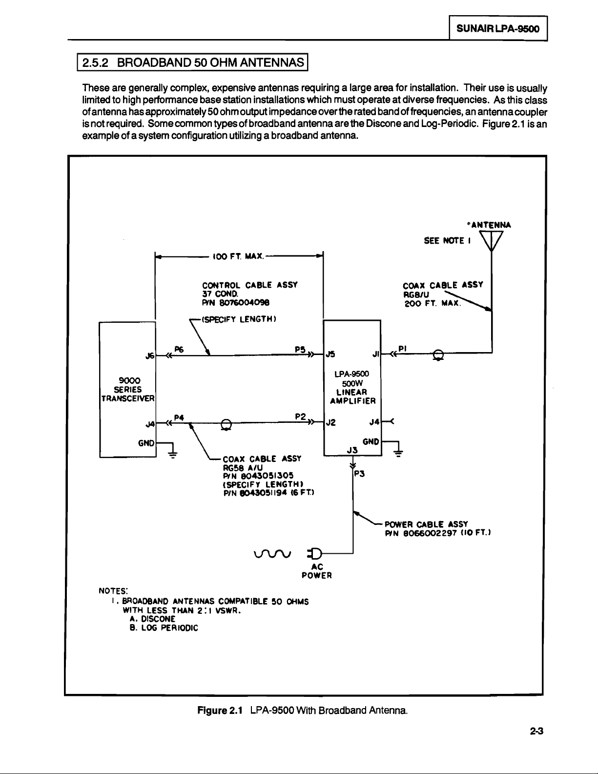
12.5.2
These
limited
of
antenna
is
not
example
BROADBAND
are
generally
to
high
perfonnance
has
approximately
required.
of a
Some
system
~---
50
OHM
complex,
base
50
common
ANTENNAS
expensive
station
ohm
output
types of
broadband
antennas
installations
configuration utilizing a
100
FT
MAX.----~
CONTROL CABLE ASSY COAX
37
CONO.
PfN
8076004098
:SP£CIFY
LENGTH'
1
requiring a large
which
impedance
antenna
broadband
must
over
the
are
the
antenna.
area
for installation. Their use
operate at diverse frequencies.
rated
band offrequencies,
Discone
and
Log-Periodic.
SEE
CABLE
AG8IU
200
FT.
NOTE
ASSY
MAX.
an
antenna coupler
~ANTENNA
I
As
Figure
is
usually
this class
2.1
is
an
9000
SERIES
TRANSCEIVER
GND
NOTES:
I.
BROADBANO
WITH LESS THAN
A.DISCONE
B.
LOG
J6~*(~~~~
J4
PERIODIC
__
1-
____________
(P4
~
.,.
~COAX
ANTENNAS COMPATIBLE
2:
I VSWR.
CABLE
RG58
AlU
PtN
8043051305
(SPECIFY
PIN
804305119.
~P5~"~J5
P2,
ASSV
LENGTH'
(6 FT.l
POWER
50
OHMS
AMPLIFIER
J2
AC
LPA-9500
soow
LINEAR
JIH~P:..:I
__
POWER
PfN
8066002297
CABLE
Pt
___
ASSY
....J
(10 FT.)
Figure
2.1
LPA-9500
With
Broadband
Antenna.
2-3

~a~S~_i~?~a
SUNAIR
L
LPA~9500
______
I
~.
____________________________________
___
I
I
:::
III
j
2-4
Figure 2.2
I
:::
I
t
:1
Cl
LPA-9500
;
W/CU-91
e
i!
it
:II
I~
!
~
~I
'"'
I
Ie
;:
1111
1-
I; _
i~!;
~i
J!
00,
35 FtAntenna (RoofTop Installation).
i!!1
~
wi
.
i!111
I~I:!
!
1111
i

en
c
~
::u
~
i
M1BIIA
,
...
t:
i
• I
MX.
II£CIlfIfJIJED
fT.
FT.
150
101
\1lTMiE
IlDiII
I-
u
-
..
C»tIOIt
ASSY
8&911&1I!I!I
lElliiTHI
PII
CMlE
ISP£[]FY
I681U
COAX
1f.RIUIW.
~~W:al
IIII10IIA
...
~
I
EI
.,
CIIftD
.....
=
)>1.
ISSY
I'f
C_
_
I
lElliiTH
819i!SOOll!li
1M
SPEt:lFY
I
P
~
FTI
110
ASSY
CABlE
8D660OCZ97
PIlIiER
PIN
MX.
fT.
258
I.
ASSY
CMlE
•
FTMX
..
I
311lNJ
eut_
1-
."
11
JS
(f.I
f'5
l£Jl61111
8016004098
PIN
s!ll>ttlFy
..
K(
J6
ca
I\)
c."
if
c
z
o
::::J
J41_«'4
500W
IIIIfllFlElI
UII£M
LPA-9!500
J2
»-1
I'f
Q
/
~
P4
9000
TR.Gm:~
::::J
Sl)
~
:D
-------=-.:..I-fJ.
;a
~
ASSY
CMlE
COAX
L
':"
::::J
::::J
!»
1"3
Fn
II;
lEH6THI
AIU
8043051305
8843051194
ISPEtlFY
R6S8
PIN
PIN
It.
PIlIiER
\.fVV
~

SUNAIR
LPA-9500
HALVARO
INSUI,..ATOR
ANTENNA
75·150
FT.
(CUSTOMER
SELECTS
WI
RE
LENGTH)
20
FT.
MINIMUM
6
FT.
GROUND
POST
ANTENNA
HEAV'"
COUPLER
STRAP
DETAIl,.
._
........ok•
.----
.,.
..........
.
ANTENNA
(l,.OOP
TWICE)
A
WIRE
THROUGH
2-6
Figure 2.4
KW
Longwire
Antenna
Kit.

SUNAIR
LPA-9500
2.6 EXTERNAL
12.6.1
The
Whenever possible, the primary power source
ampere capacity,
type
primary power interconnect
three
black
described. The
12.6.2
Separation
is
fumished
jacketed. This cable
The
is
N
PRIMARY
LPA-95oo
will
insure that
each
NO.
and
the white wires connect to the
TRANSCEIVER
between
shown
adequate for transceiver
OS8864ooo0
in
Figure
with
RF
coaxial cable
CONNECTIONS
POWER
requires a
manual
all
10
AWG
standard
primary
disconnect
power
has
diagram
conductors. The
cable
CONNECTIONS
thetransceiver
2.S.
The
transceiver accessory
the
LPA-9Soo.
is
available
is
also
available
to
should
be
used.
CONNECTIONS
power source that
switch
been
forthe line voltage
as
fumished is 10 feet
and
The
control
in
lengths specified
in
amplifier spacings of
Connector kits are provided
I
can
should
(40 ampere
removed
from the unit prior to entrance for servicing. Referto Figure
green
wire
con
115
or
230
I
the amplifier
cable 0579240002
lengths specified
may
plug,
less
provide
be
connected
if
primary source is 115
connection
nects to the station primary power ground system.
volt
long.
be
PS,
by
the
by
than 50feet. For distances
up
to 2.5
kVA
(115
or
230
VAC).
to
the amplifier
details. The Power
power
source at the disconnect switch previously
up
to
150
feet.
The control cable to the transceiver
is
fumished
is
37 conductor, NO. 20
customer.
the
customer.
with
the
with
Type
LPA·9Soo
through
VAC).
Gable
the transceiver. The
RG-58A/U,
above
and the transceiver.
a double-pole,
An
arrangement ofthis
Assembly contains
AWG
wire,
PIN
50
feet, RG·8A/U,
shielded
0588130001
plug
The
PS,
and
20
2.S
"'
is
PI
12.6.3
Theamplifier's RFoutput connector isalsofumished
regardless of the distance to the antenna or antenna coupler.
RF
OUTPUT
CONNECTIONS
{
LPA-9600
Figure 2.5
GRC
AC
AC
LINE
LINE
Power
1
in
the Connector
J3
-
A
-
B
~
C
'"'"-
Cable Assembly
1'3
-
~
!--
""--
A
B
C
GREEN
BLACK
WHITE
PIN
Kit.
RG-8A/U
}
PRIMARV
POWER
115/230
'%15%
50
to
8086002297.
coaxial
VAC
50
HZ
cable
should beused,
2-7

SUNAIR LPA-9500
':"kea
_
076100003~"
~£'E>?i
aa
AT-gOOD
39
PIN
PH.
CPWD8F-20-39P)
CONNECTOR
1011130009
A)~
____________________________
B)
C)
~
E)
F)
G)
H)
J)
Ie)
L )
w)
N)
P)
A)
S)
T)
U)
~
W)x
X)
Y)
Z)
A.>
~
!:>
~
CABLE.
37
PH.
·~2~B~V~TUN~E~E~N~A=B=LE~
ICW
ICW
cbNOUCTOA.
057924000e
COUPLE
A gETECT ( J
~
IIADLT'
6
CHANNEL
qtANNEL 21 ( Z
CHANNEL
CHANNEL
ICW
!'"OWEA
I'IeFLE(:TEO POWE.. <
TUNE
ICW
ICW
pDWE..
BAND 8 seLecT
BAND 7 SeLEct
BAND 5 seLecT
BAND 3 SeLeCT
BAND 1 SeLeCT
2
2·
e·
SELECT (
CCMotAND
ALC
ACC
DETECT 1
kEY~SDRY
ItW OIHII:t;T P
TUNING
CHANNEL
CHANNEL
CHANNEL
ICW
FI ( W
2i
27
oN
.20
___________________________
LPA-9500
37
PIN
PN.
CMS3106A-eB-~lS)
CONNECTOR
0754320006
--«S
( N
w
'e
( U
<
!:!
( T
~
~
<
IC
<
~
<
~
(
!:
( H
<G
<E
(C
(
~A
(
<
( L
(!
<x
(A
D
~)
G
-)~---------------------------~BA~ND~~O~s~e~L~e~C~T~~---------------------------~
~)
!>
:!.>
9
~
~
~)
9)
~)~
______________________________
leW
POWER
BAND 8 seLecT
BAND 2 SeLeCT
BAND 4 seLecT
GROUND
CHANNEL
leW
.=26~V~D~C~(~2~W~IR~E~S~I~---------
OliTECT 2 ( E
C 2 WIRES I ( 0
2 • (
FORWARD
POWER (
_______________
(
( F
<B
(V
~(!
-
~
~
!:
Figure 2.6 9000 Series Exciter{Transceiver To LPA-9500 Control
Cable.

12.6.4
When
or use
ANTENNA
an
antenna
control
cable
COUPLER
coupler is
assembly
CONNECTIONS
to
be
used,
cable construction
PIN
8092500096 (specify length)
I
is
accomplished
see
Figures
using
2.2
connector
and
2.3.
PIN
1008390011
12.6.5
Grounding
RF
lengths
STATION
terminals
ground
system.
to a minimum.
RF
Use 1or 2 inch
~
GROUND
are
provided
SYSTEM
on
the
transceiver,
wide copper
CONNECTIONS
LPA·95oo
strap
or
NO.6
2.7 PRELIMINARY CHECKS AND APJUSTMENTS
Determine
necessary to
Al
OSl. is
If the
Otherwise, set the power levels
from
change
in
the
LPA·9500
a)
CW,
b)
watts
the
voltage
proper
is
received asa
Set
LPA-9S00
Set
out.
customizing
voltage customizing are
position.
system
transceiver/exciter frequency
to
SOOW.
transceiver/exciter
with
as
follows( see
Key
label
the
proper
shown
its
companion
transceiver/exciter
to
AM.
in
Figure
to
14.2000 MHz.
Key
transceiver/exciter
line voltage forthe unit
Figures 2.7
transceiver/exciter, noadjustments
5.1
for component locations}:
and
I
and
antennacouplerforconnection tothe
AWG
wire
or
larger
for
this
bonding.
being
and
2.8.
Be
Set
transceiver/exciter
adjust
A3A2R33
and
adjust
installed.
sure that the
for
A3A2R43
500
Connection
Fan
should
MODE
watts
for
Keep
Voltage
be
necessary.
to
out.
200
station
lead
changes
Switch,
2.8 BACK MOUNTING KIT OPTION
An
optional
racks.
slide
See
Figures 2.9
rack
mounting kit is available to facilitate installation ofthe LPA·95oo
and
2.10.
in
standard
E.I.A.
equipment
2-9

t
~aMS~b~~.~~a
SUNAIR
LPA-9500
__________~.............................
I
________
....__....__........__....__............__............
SEE
DETAIL A 8 B
_
2-10
BlK
WHT~~~
DETAlL
230VAC
Figure 2.7
CIRCUIT
Voltage
A
BREAKER
Customizing
WIRING
AUXILIARY
POWER
SUPPLY
SWITCH
WHT
- Circuit Breaker/Auxiliary
BLK_
JUMPER
115VAC
CIRCUIT
DETAil 8
BREAKER
Power
WHT
WIRING
Supply.
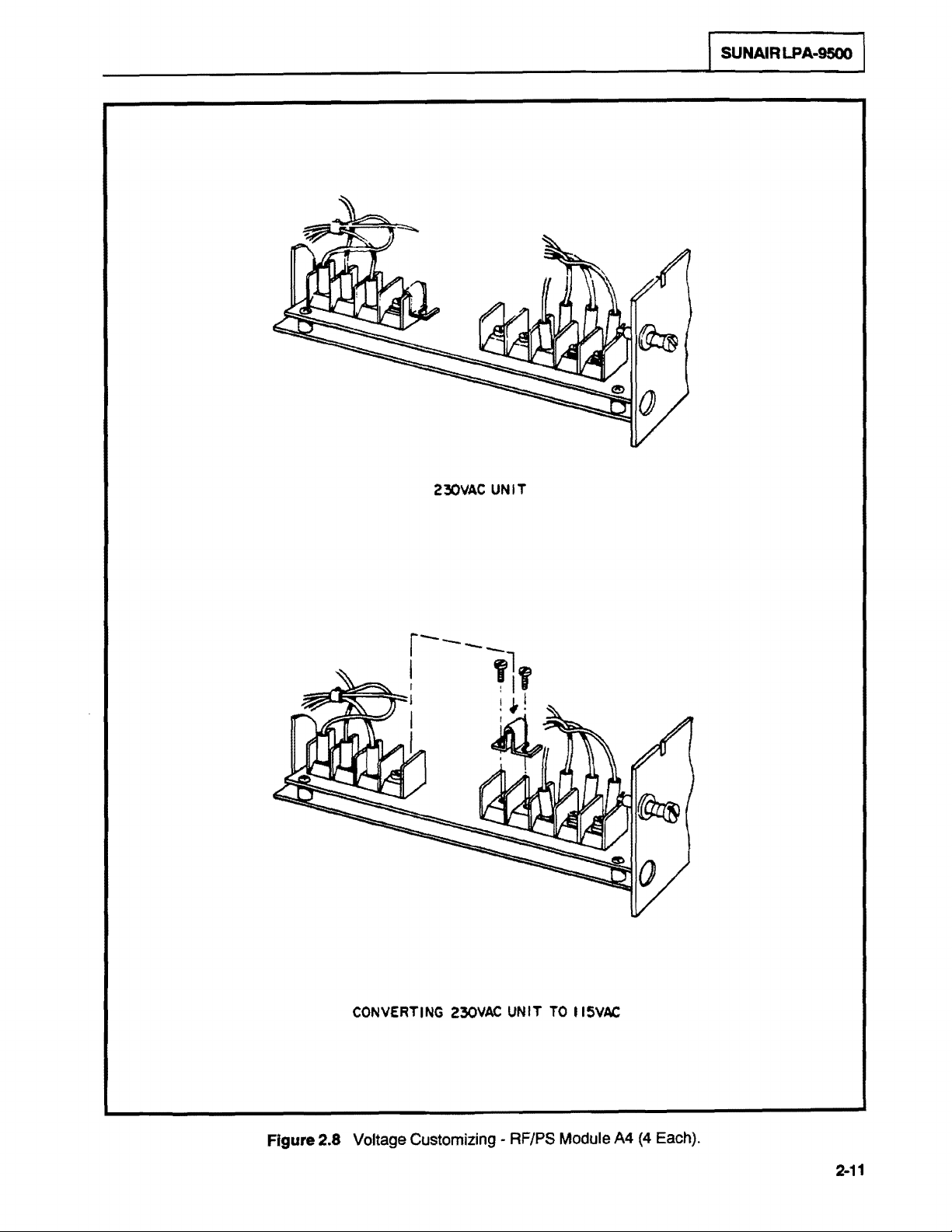
ISUNAIR
LPA-9500
I
230VAC
UNIT
CONVERTING 230VAC
Figure 2.8 Voltage
Customizing
UNIT
- RF/PS
TO
115VAG
Module
A4
(4
Each).
2-11

I
SUNAIR
LPA-9500
I
2-12
RACKMOUNTlNGKJTLPA-9500
SUNAIR
SUNAlBPJN
80660042XX
50660043XX
6032041204
0538750006 Nut, Clip 10-32
0538870001
1002860032
PIN
80660042XX
Back
Mounting
Bracket,
Chassis
Screw,
Shim,
Plate
PESCBIPDQN
Rack
Slide
Ornamental 10-32 x 1/2 L
LPAIPS
Figure 2.9 Rack Mount Slide Details.
Kit
Mounting

I
SUNAIR
LPA·9500
Figure 2.10.1 Shock mount Equipment
Rack
With
Outline Dimensions
And
Details (Sheet
1/2).
2·13

"'--
• •
'rOI'
....
BLANK PANE!.'
EXCITER------f+I~
IlI.ANK
POWER
AIIlPUFIER
BLANK
PAM£l-----+H-
NOTE: IMOCICIIOUNT 0f'T1ON
--oc:::::::U==~-----=~
PANEI.----+l+-
-----+lH-
INC:AEAIU
2112"'
HlIGHT
IV
....
....
••
e.
lit"
'"
2·14
SHOCKMOUNTKlTEQUIPMENT
ITSMNQ SUNAlBPIN
1
2
3
4
5 1001280016
6 1001290003
7
8
0501650008
0501700005
0542880644
0841810001
1001300009
1002980011
RACKSUNAIR
PIN
6032090892
PESCRlP'DON
Washer, Split 3/8
Nut, Hex 3/8-16 X 9/16 AF
Bod,
lhd
Hex
3/8-16 X 4
5/8-11,
Instructions
Isolator, ShockNib. 50-80 Lbs
Isolator, ShockNib. 100-155 Lbs
Bolt,
Washer, Split 5/8
Installation
Lg
1"h1/2
Lg
2
4
2
2
4
4
4
1
Figure 2.10.2 Shockmount Equipment Rack With Outline Dimensions And Details (Sheet 2/2).

LPA-9500 LINEAR POWER AMPLIFIER
INSTALLATION WARNING
If the LPA-9500
9600
power
1.0 Turn the LPA-9500 Circuit Breaker (A8CB1) OFF.
2.0 Turn the RT-9000 power ON.
3.0 Set each operating channel position to
the value.
4.0 Turn the LPA-9500 power
with the desired RF power levels.
(1
kW) Amplifier, accomplish the following procedure before turning the LPA-9500
on.
is
installed with a RT-9000 that has previously been operating with a LPA-
125 WATTS. Press the ENTER key to store
ON and program the RT-9000 operating channel positions

I
SUNAIR
LPA-9500
I
SECTION
III
OPERATION
3.1
GENERAL
This
section
Solid
and
Maintenance
State
provides
Power
information
Amplifier
Manuals
and
for
detailed
and
instructions
an
automatic
antenna
information
required
coupler.
regarding
for
operation
Refer
operation of
ofa
transceiver,
to
the
these
transceiver
units.
the
and
3.2 FUNCTION AND LOCATION OF CONTROLS AND INDICATORS
Table
3.1
lists the controls
and
indicators
of
the
LPA-9500
front
panel.
Locations
are
shown
3.3 OPERATING THE LPA-9500
13.3.1
Insure
and
OPERATION
that
the
transceiver/exciter
in
the
radio
manual.
WITH
If
an
antenna
9000
and
SERIES
the
LPA-9500
coupler
EXCITERITRANSCEIVER
are
is
being
installed
used,
properly
insure
its
by
referring
proper
I
to
installation
LPA-9500
the
coupler
in
Figure
Section
II
also.
500W
Operation
3.1.
in
this
Linear
manual
a) Apply
b)
On
LPA-9500,
1.
power
Without
to
the transceiver/exciter
POWER
an
lamp
automatic
will
antenna
light
and
LPA-9500.
and
LCD
coupler,
will
display
"SYSTEM
system
OPERATIONAL,
5OOW'.
2.
With a CU-91
00
antenna
coupler,
"FAULT:
COUPLER
UNTUNED,
5OOW'.
c)
d)
e)
~
OPERATIONAL".
1.
Without
ready
to
operate. Ifinstead
Reset
the
LPA-9500bytumingthetransceiver/exciteroff,
9500
tum circuit
If
FAULT
dthroughfbelow. v
Select
Depress
On
antenna
Series
does
2.
With aCU-9100antenna
operating
'CPLR
LPA-9500,
1.
If after tune
orfeeclline.
or coupler
an
breaker
not
clear.
frequency
TUNE'
LCD
will
After
completion
manual.
automatic
the
OFF
see
on
button
display
attempt.
Attempt
antenna
FAULT
then
Section
coupler
transceiver/exciter.
on
system
oftune.
FAULT
retuning.
coupler,
lamp
on
ON;
or
using
V
of
this
FAULT,
the
9000
Series
messages:
(maximum 2 seconds)
lamp
on
LPA-9500
If
FAULT
'SYSTEM
the LPA-9500llashes, this
the
PWR
manual.
the
LPA-9500
Front
"COUPLERTUNING",
does
OPERATIONAL'
wait
30
LVL
key
FAULT
Panel.
system
bums
steadily,
not
clear,
seconds,
on
see
message:
indicatesafau
then
the
keyboard,
lamp
"COUPLER
is
ready
this
indicates
Section
METER:
METER:
is
displayed
tum
will
bum
for
operation.
Vofthis
FWD,
FWD,
It
in
back
on; orat
reset
steadily.
TUNED".
a fault
manual
PWR
PWR
and
system
the
LPA-9500.
the
LPA-9500.
Follow
"SYSTEM
in
the
and
the
LVL:
LVL:
the
LPA-
steps
coupler,
9000
is
~~
..
7t.:LIDid
0G
...
3-7t
};:MO.LN:iI~~~}{'17t

SUNAIR LPA-9500
2.
If FAULT lamp on LPA-9500 flashes, this indicates a fault in the LPA-9500. Reset LPA-9500.
FAULT does not clear, see Section V
I
NOlC:
I If an antenna coupler is not used, tuning is not required when the
of
this manual.
operating frequency
of
the transceiver/exciter is changed. With an
antenna coupler, coupler tuning is required with each frequency
change.
If
LCD
CIRCUIT
~
•••
Mt"~~
l
..
.,....,-.~
d~~I~lIo,~
'"
,~,-"'"
BREAKER
.""'~
3-2
KEYBOARD FAULT LAMP
Figure
3.1
LPA-9500 Controls And Indicators.
POWER LAMP

ISUNAIR LPA·9500 I
Table
CONTROL
Meter, A2M 1
LCD Assembly, A2A2
Circuit Breaker,
FAULT Lamp, ASDS2
POWER
Keyboard, A2A 1
OR
Lamp,
INDICATOR
ASCB1
A8DS1
S1
3.1
Controls
And
Indicators - Front
Panel.
FUNCllON
Displays the following:
1.
0 -650: Forward Power
2.
0 -140: Reflected Power
3.
0 -
6OV:
Selected PA's voltage
4. 0 -18A:
This Uquid Crystal Display (LCD) displays all systems messages and
conditions.
Applies primary power to the r.PA-9500.
A
red
fault lamp which, when flashing, indicates a fault
steady fault lamp indicates a fault external to the LPA-9500.
A green lamp which indicates that primary power has been applied to the
LPA-9500.
The keyboard affords the operator/technician the ability to check individual
voltage, current and power levels. The keyboard also provides the operatorl
technician with the ability to select desired power operating levels and to
failure indications.
Selected PA's current
in
in
watts
watts
in
the LPA-9500. A
read
1.
Ic#1:
PAII1
on
meter.
2.
Ic#2:
PAII20n meter.
3.
Vc#1:
PAII1
on meter.
4.
Vc#2:
PAII2
on
meter.
5.
FWD:
watts on meter.
6.
REFD:
in
watts on meter.
7.
PWR LVL: When depressed changes output power
level reading on LCD Assembly from 1 kWto 500 watts to 1 00 watts
(bypass). Also used to reset LPA-9500.
8.
*:
'Fault: MULTIPLE..PRESS
fault message. A different fault message will be displayed each time
the key is depressed until all faults detected have had messages
displayed.
When depressed displays power supply current of
When depressed displays power supply current of
When depressed displays power supply voltage
When depressed displays power supply voltage
When depressed displays forward output power
When depressed displays reflected output power
When morethan one fault occurs, the LCD Assy will read
*'.
Depress this key to display each
of
of
in

I
SUNAIR
LPA·9500 I
•
ITHIS PAGE INTENTIONALLY LEFT BLANK. I

4.1
GENERAL
Refer
to
Figures
The
LPA-95oo isan
transceivers
combining
operation ofthe
In
addition
or
shuts
The
RF
combiner,
RF
modules.
over
300
combiner,
harmonic
frequency
so
that
or
networks,
to
reporting
it
down
circuitry
and aharmonic
watts
providing
outputofthe amplifiers byat least
span
no
tuning
THEORY OF OPERATION
4.1
and
5.4.
all-solid-state,
exciters.
unit
completely,
consists
Each
power
(1.5 xfrequency),automatically
is
The
harmonic
and
report
malfunctions,
of
low
RF
amplifier
output
over
600
required.
self-contained,
unit
is
complete
filters
and
malfu.nctions
the
providing
an
input
power
pass
filter.
module
capability.
watts
output
microprocessor
microprocessor
exciter
consists oftwo
The
SECTION IV
500
watt linear
in
one
package
control
in
English
only
splitter,
The
input
output
capability
75
dB.
language
reconfigures
operation.
two
broadband
power
conservatively
from
the
in
one
The
filter
selected bythe exciter
and
splitter
two
RF
feedline.
is
split
power
amplifier
includes
circuitry.
on
a front
the
RF
power
divides
rated
amplifier
The
into8bands,
and
SUNAIR
designed
RF
amplifier
Built-in
panel
the
diagnostics
liquid
amplifier
modules iscombined
harmonic
buffered bythe
to asafe
amplifier
exciter
power
amplifiers
each amaximum ofone-half octave
for
use
modules,
monitorth,functional
crystal
power
low
alphanumeric
operating
modules,
equally
combined
pass
microprocessor
with
power
an
output
among
in
the
output
filter attenuates
LPA-9500
9000
Series
supplies,
display.
power
level,
power
the two
to provide
power
the
circuitry,
Each
power
amplifier
powersupplies
RF
module
bias
control
voltage to
module
are
high-efficiency
assembly
the
dual
amplifier,
consists ofan
switching
provides
microprocessor-controlled
ensuring
RF
regulators,
linearity.
4.2 CONTROL PANEL MODULE A2
Refer
to
Figure
The
Control
LCD
Assembly.
diagnostic
the
meter
keyboard
Computer
9500.
The·
currents,
5.5.
Panel
Module
and
the
informationI and
display
to
four
close
MOTH
key
is
collector
functions.
the
proper
ERBOARD
used
to
voltages,
is aplug-in
3 x 4
keyboard.
the
function
The
.row
A3A
scroll
through
panel
PC
Assembly
to
the
1.
The
and
either
arrangement
The
LCD
selected
proper
PWR
LVLkey
multiple
forward
module, a power
with
built-in
on
the front ofthe
Assembly
to
be
Control
column
fault
indications.
or
reflected
A2A1 is
displayed
Panel
when a key
is
used
supply,
AC
on
A2A2
to select
The
power.
and
currentfoldbackand
power
inputtothepowersupplies,
LPA-9500
used
the
meter.
provides
is
depressed
the
desired
meter
an
RF
module
to
display
The
3 x 4
the
interconnections
and
pass
operating
is
used
to
display
control
overvoltageprotection.
which
contains
the
power
keyboard
the
power
any ofthe
assembly.
and
the
level
selected,
is
used
which
information
level ofthe
four
meter.
permitthe
The
The
regulated
the
the
to
select
on
to
the
LPA·
collector
4-1

I
SUNAIR
LPA-9500 I
4.3 COMPUTER ASSEMBLY
14.3.1
Referto
The
Microprocessor
Microprocessor
Connector
interfaces
A3A
front
overtemperaturefan.
14.3.2
Refer
4.3.2.1
The
fault indicators
A3A3U1
interface it
PC
ASSY
Figure
Computer
1 J4 interfaces
panel
5.6.
MOTHERBOARD
Board
Board
A3A 1
J1
to
the Filter
of the
PERIPHERAL
to
Figures
GENERAL
Peripheral
when afault
4.2
BoardA3A2
and
with a CU-91
COMPUTER
A3A3
and
plugs
into
provides
with
LPA-95oo
routingforthe signalstoand
Module
the
AS.
transceiver/exciter
by
BOARD
and
5.7.
contains
detectors
has
are
occurred
00
Digital 1OOOW
A3A1J6
transferring control
located
A3
MOTHERBOARD
acts
as a back
to
interconnect these two
and
Connector
A3A21
much ofthe
on
this
in
the
electronic
Coupler.
plane
A3A1J7.
A3A 1 J3
and
the
signals
analog
board.
operation
A3A
11
to interconnect the Peripheral
boards
The
Peripheral
from
the
power
connects
antenna
circuitry
These circuits
coupler.
to the front
used
of the
to
the balance of the
Board
ampl
ifier
to the Control
Connector
panel
..
to
monitor
are
designed
LPA-95oo.
plugs
assemblies.
Panel
and
Also
into
A3A
lights,
control
to
provided
Board
A3A
Module
1 J5 interfaces
the
the
inform
A3A2
LPA-95oo.
1 J8
and
Connector
A2.
bypass
LPA-95oo.
Microprocessor
are
circuits
to
the
The
A3A1J9.
A3A1J2
Connector
with
the
relay,
and
Many
which
The
Peripheral
1.
The
it
from
producing
2.
The
DETECT 2 operate
3.
The
4.
The
attached
The
Peripheral
keyboard
the
front
panel
lamp)backlightfornighttimeviewingoftheLCDAssembly.Alsoprovided
monitors
of
ALC orACC
4.3.2.2 TEMPERATURE SENSE COMPARATORS
The
purpose ofthe
on
the
two
amplifier
speed.
Ifthe temperature continues
Board
signal
signals
signal
signal
and
is
Board
to select
LCD
the
forward
needed
individual
heatsink
is
responsible for
BYPASS
READY
used
+28
tuning.
Temperature
reaches
which
its
power
REMOTE,
circuits
to
drive the
VDC
contains
meter
functions.
Assembly.
and
reflected
to
control
power
between
the
causes
output.
in
the
TUNE
the multiplexer circuits
Similarly, a OCto
Sense
amplifiers
the
KW
DETECT,
9000
Series
fault
lamp
ENABLE
Contained
power.
the
9000
Comparators
has
reached
75°
and
to
increase
This
following
LPA-95oo
on
which
Series
85OC,
functions
to
be
FAULT
Exciter/Transceiver.
the front
also
AC
circuit
and
panel
instructs
which
is a DC
inverter
is
responsible for selecting
equipment
U1,
isto
detect
either of two
Microprocessor
reaches
required
bypassed
REMOTE,
of the
LPA-9500.
the
transceiver that a
permit
to
DC
converter to provide contrast adjustment for
is
provided
attached
U2
when
the
thresholds.
A3A3U1
between
for proper operation of the
in
KWPOWER
ten
which
to the
temperature
1 oo°Cto
the
event of a
of the twelve front
drives
is
the
LPA-9500.
When
causes
1200C,
fault
DETECT
CU-91
the
EL
ALC/ACC
and
producing
on
anyofthe
the temperature
the
fan
A3A3U1
LPA-95oo:
which
in
tum inhibits
1,
and
KWPOWER
00 antenna coupler
panel
keys
on
(electroluminescent
Control
to operate at a higher
Circuit
the proper
two
heatsinks
on
any
power
shuts
down
which
level
the
is
the

I
SUNAIR
LPA·9500 I
overheating
4.3.2.3
The
purpose ofthe
the temperature of
monitor a
If this
In
addition,
4.3.2.4
power
OVERTEMPERATURE
Signal
called
signal
is high,
A3A3U1
GAIN
FAULT
•
The
Gain
Fault
Comparators
power
amplifier
power.
4.3.2.5
The
power
message
BYPASS.
will
If the
Gain
amplifier
place
GAIN
assemblies.
power
FAULT
Fault Buffer
assemblies.
to
be
displayed
The
signal
LPA-9500
amplifier.
BUFFER
Overtemperature
power
amplifier
FILTER
A3A3U1
will
COMPARATORS
amplifier is
BUFFER
is
the
VSWR
in
BYPASS.
force
device
on
MODULE
will
cause
the
are
a series of two detector circuits
The input
not
U7
When
the
LCD
FAULT
protecting it
U3
BufferU3
assemblies
FAULT.
an
indication
LPA-9500
U12
power
producing
by
which
any
of the
Assembly
is
also
isto
provideameans bywhich
1,
and
2.
U3
also acts
This
Signal
originates
on
the
LCD
to
BYPASS
to a particular
the
required
Microprocessor
GAIN
A2A2.
monitored
from
operation
power
amountofpower,
A3A3U1
FAULT
At the
by
A3A3U1
the
excessive
signals
Assembly
to
protect the filter
used
to monitor
amplifier
monitors
go
same
time
thru
VSWR.
Microprocessor
as a position
in
the
Filter
pointing
assembly iscompared
Microprocessor
high,
A3A3U1
U7.
If this
from
Fault Detector
out
the
module
the
power
the status ofthe
A3A3U1
will
will
place
Signal
A3A3U1
which
faulty filter
gain ofthe
A3A3U1
goes
can
A3A3U1
U9C,
from
to
gain ofthe
cause a gain
the
LPA-9500
high.
monitor
can
U20A.
module.
damage.
individual
its
output
is
alerted.
two
fault
A3A3U1
in
4.3.2.6
The
are
volts,
from
4.3.2.7
The
by
ifthe voltages are
4.3.2.8
U19
that is
voltage
A3A3U1
VC
MONITOR
purpose
mounted
theoutputofU11
operation.
purpose
the logic
is
too
of the
in
VOLTAGE
of the
control
VC
MONITORNOL
used
by
low.
is
too
high
takes appropriate
each ofthe
Microprocessor
U19
COMPARATORS
VC
Monitor
goes
MONITOR
Voltage
circuitry
too
high
is also
or
too
Comparators
power
high.
Monitor
in
the
ortoo
TAGE
used
low.
A3A3U1
action
U11
comprising
amplifier
Microprocessor
COMPARATORS
Comparators
LPA-9500.
low.
MONITOR
A3A3U1
to
determine ifthe
and
assemblies.
Microprocessor
BUFFER
to determine if
periodically
alerts
the
operator
U11 isto
When
A3A3U1
U13
comprising
+28V
will
U19
any
logiC
samples
to
monitorthe
the
voltage
sense
this
and
U13
is
to
monitor
A3A3U1
of the
control
the inputs of U
the
monitorstheoutputsofU13todetermine
+48V
power
voltage
condition.
individual+48V
in a power
remove
the
is
too
19.
supply falls below
the
defective
+28VDC
supplies
low
or
If
any
of
power
supplies that
power
and
+5VDC
is
prodUCing
ifthe
+5
V logic
these inputs
+42.3
supply
utilized
a voltage
control
are
high,

ISUNAIR LPA-9500 I
4.3.2.9 COLLECTOR VOLTAGE METER CONDITIONING CIRCUIT U14
U14
functions
U
14C
conditions the
for
PA
#4.
function
divider
Multiplexer
resistance)
reduces
as
four distinct
(PA
#3
and PA#4
identically.
the
+48V
(approximately
causing a +48V
+48V
For
example:
identical
for
PA
are
not
to
+3V.
470
indication.
#2,
installed
For
which
ohms
stages.
U14B
conditions the
in
the
PA
#1
,+48V
when
applied
resistance),
(Full
scale
U14A
conditions the
+48V
for the
LPA-9500).
is applied
through
supplies approximately
on
the meter is
These circuits are voltage follower circuits
to
U14A
a 33.2 k
+48V
100
from
PA
#3,
through
ohm
resistor
80
IJA.)
PA
#1
for display
and
U14D
conditions the
a resistor divider.
and
U17,
the
IJA
to the meter
on
the
meter,
+48V
which
The
resistor
16
Channel
(3.7 k ohms
4.3.2.10 COLLECTOR CURRENT METER
The Collector
Voltage
inverting amplifier
of conditioning the voltage
assembly
deflection of the meter is equivalent
deflection
section of U
4.3.2.11 16CHANNEL
The
purposeofthe 16Channel
to
the
front
selection
4.3.2.12 MULTIPLEXER SWITCH SELECTOR LATCH U18
The
purpose ofthe
can
sel
ect
inputs
to
Meter
and
would
16.
panel
which
the
U17
Current
Conditioning
producing
proper
to
Meter
which
indicate
meter as they
enables
Multiplexer
meter
cause
U17
Conditioning Circuit performs a function similar
Circuit
inverts a minus voltage
which
a proportionate current source to the meter
a half-scale
MULnpLEXER
U17
information
to
U14.
is equivalent
to 18amps.
deflection
Multiplexeristo
are
selected
to
select the proper
Switch
select
the
CONDlnONING
U16
is divided into four sections, A thru
to
resulting
U17
provideameans bywhich
by
the
Selector
to
be
senttothe
proper
Latch
keyboard
plus voltage for indication
to
the collector current
If a
power
amplifier is
from aSOIJA
keyboard.
analog
gate circuit
is
to
provide a
front
panel
selected current
CIRCUIT U16
being
to
deflect
drawing
current
different
Microprocessor
output
means
meter to
be
source
to
that
performed
D.
on
the
meter.
drawn
it
the
proper
a current of 9
source
to
by
displayed.
produced bythe
current
A3A3U1
be
supplied
which
to
by
the Collector
and
acts as a unity
Each
one
by
each
power
amount.
amps,
concerned
sources
provides
Microprocessor
U18
be
supplied to the
can beapplied
binary
to
the
meter.
provides
gain
is
capable
amplifier
Full
scale
the meter
input
A3A3U
the
binary
m"eter.
1
4.3.2.13 OVERCURRENTDETECTORSU15
The
Overcurrent
PA#1, U15B
installed
assemblies
to
operation,
4.3.2.14 LCD
A signal called
used
LCD
BAD7.
in
the overcurrent
by
the
Assembly
Detectors
monitors
the
LPA-9500).
respectively.
condition
reducing
LCD
the
ENABLE
LCD
E is
Assembly
where
are
comprised
PA#2,
output of the
produced
itpermitsthe
U15C
The
detectors are set to detect a condition of
If a
power
amplifier isdrawing
by
U15.
INVERTER U6E
on
A2A2
as
LCD
of four
monitors
Once
the
LPA-9500
the Microprocessor
an
enable.
to
read
identical
PA
#3.
condition
from
U6E
or write information
and
too
much
is verified,
1000
Board
inverts
circuits
U15D
current,
to
500
A3A3
the
U15 A thru
monitors PA#4. (PA#3
then
watts.
and
signal
from
D.
U15A
monitors the current
17.5
amps
in
the four
then
Microprocessor
A3A3U1
needs
to a signal
orto Address/Data
removes
to
be
inverted
called E and
and
PA#4
are
not
power
amplifier
A3A3U1 isalerted
that amplifier
before itcan
sends it
Bus
BADO
from
be
to
the
through
in

I
SUNAIR
LPA-9500 I
4.3.2.15
The
indicating
A3A2R56.
established
4.3.2.16 FILTER FAULT
The
available
it.
U20Amonitors the
from
high
amplifier
4.3.2.17
The
If
power
When
producing
these
VSWR
purpose
that
purpose
is
the poweramplifiers
for
longer
assemblies,
RF
RF
Present
is
present
Microprocessor
only
FAULT
of
the
VSWR
action
is
U9B
compares
by
R56.
the output of
of the Filter Fault
malfunctioning
forward
than
50
preventing
PRESENT
Detector isconnected
on POUT
A3A3U1
power.
if
RF
Since
is
present.
required.
ms,
DETECTOR
Fault
Detector
U9B
the
ratio
of
U9B
DETECTOR
Detector
in
such a way
power
leaving
with
the
power
then
A3A3U1
them
DETECTOR
MONITOR, Q4will
certain
Q4
tothe
detects
faults
U9B
is to alert Microprocessor
may
be
adjusted
FWD
PWR
goes
high
USC,
U20A
is
to
wam
that
power
the LPA-9500.
leaving
causes
from
damaging
Signal POUT
the
low,
can
only
the
betumed
then
be
to
trip
to
REFD
alerting
Microprocessor
the
legitimate faults
A3A3U1
is
being
LPA-9500.
LPA-9500
the
filter
MONITOR
on,
It
knows
A3A3U1
on
VSWR
PWR.
sent
U9Ccomparesthe
A3A3U1
to
module.
producing alow
through
faults of2:1 or 3:1
When
REFD
of the excessive
A3A3U1
into the filter
monitors the
go
to
BYPASS
as
is
U9C ofthe
on
its
software that
in
the presence of
that a
PWR
when
one
assembly
power
by
US,
the
VSWR
VSWR.
entering
outputofU9C
shutting
Filter
RF,
fault
is
occurring.
using
potentiometer
exceeds
of the filters of the eight
but
Fault
Coupler
the
power
A3A3U1
the threshold
is
not exiting
the filter
and
down
the
Detector
Interface
amplifiers
will
modules
if it
circuit.
Buffer.
monitor
from
goes
power
are
•
4.3.2.18 FORWARD
U23Aand
is
to
sent
A3A2U17,
front
meter
this
4.3.2.19 REFLECTED
U23B
Conditioning
the
4.3.2.20 REFLECTED FAULT
The
condition
high.
actually
013 is a
buffer the
to
two
places.
the
panel
meter
on
the
meter.
and
014
reflected
purpose
is
A3A3U1
exists.
forward
16
9000
Circuit
power
of the
occurring
POWER
peak
power
Through
Channel
of
LPA-9500.)
Series
is a peak
is
identical
information
Reflected
in
checks
and
if
so,
detector circuit
information
potentiometer
Multiplexer.
Exciter{Transceiver
POWER
detector circuit
the
LPA-9500.
the
reflected
immediately
METER
used todrive
The
other
METER
to
the
function
on
the front
DETECTOR
Fault
Detector
If the
fault
places
CONDITIONING
U1
OB.
thatthe
(R61
CONDITIONING
condition
Peripheral
A3A2R61
is
used
signal
produced
display.
used
to
of
U1
panel
meter of the
U9D
is
to
wam
reflected
the
LPA-9500
this
to
The
drive
OB.
Microprocessor
power
indicated
CIRCUIT U10B, U23AAND
U1
OB
isconfigured
Board
information
adjust
the
is
FWD
approximate
CIRCUIT
U10A.
A3A2R59
LPA-9500.
level
by
the
in
BYPASS.
receives.
is
full
scale
PWR
U1
The function of the
is
used
reaches
Reflected
as avoltage
U1
called
FWD
level
REMOTE
power
level
OA,
U23B AND
to adjust the
A3A3U1
and
OB
of
when a severe
exceeds
Fault
Q13
follower.
produces
PWR
LOCAL
FWD
PWR
which
is
of the
LPA-9500
Q14
Reflected
full
200
Detector
Its
purpose
a voltage
transferred
scale deflection of
watts,
to
which
and
goes
LOCAL
Power
reflected
on
to
is
read
Meter
fault
U9D
goes
insure that it
is
to
the
the
on

I
SUNAIR
LPA·9500
I
4.3.2.21
The
and
summation
enabling
The
ALC/ACC
is
a low it
transistors
and
at
Soo
and
U1
power
level.
the output of
the
If
the
Transceiver
ALC/ACC
purpose ofthe
to
provide
the
ALC/ACC
circuit.
means
Q1 0and
R42
would beused
watts,
ACC
voltage.
OC
is
used asa buffer
and
reflected
U1 00amplifies
LPA-95oo
outputofU20Cdecreases,
ALC/ACC
ALC
of
forward
transceiver to provide the
Control
The
that
this
high
power
Q3
will
to
compensate.
which
increases
CONTROL
feedback
and
Circuit functions
signal 1 t<YV
the
Q11
shorting out potentiometers
to
turns
to
the
level
decrease,
CIRCUIT
Control
reflected
Microprocessor
adjust the
off
amplify the
are
summed
the
Circuit
when
power
ALC/ACC
ALC
Q1 0 and
adjusted
reducing
U20B
and
the
outputofQ12
RF
power
operating
reflected
and
LPA-95oo
in
and
Q11.
by
the
U20C
U1OC,
is
to
provide
and
either
one
of two
is
Board
ACC
R33
power.
fed
to
R42,
or
ACC
amplify
supplied
U10D,
U20A,
ACC
in
SSB
or
increases
with
the
correct power output
modes.
received
wishes
control
R32and
R42
to
decreases,
to
A:3A2R33
levels.
and
R43
A:3A2A28
R42
and
the transceiver
the
to LPA-9500
BAND
feedback
CWo
It functions either
from
the Microprocessor
operate
and
now
where
R43,
and
level
red
ucing
C,
Q3
AND
to
the transceiver
The
ALC/ACC
or decreases the feedback
in
a 1000 watt
R43.
With
R33
If 1
t<YV
ALC/ACC isa
become
is
adjusted
to
part of the effect controlling the
used
to
adjust the output
all
four
potentiometers
drives
Q3.
which
increases the
by
R32
the
ALC
voltagetothe
compensate.
Q12
when
Control
level.
as a 1000
and
If the output of
or
Circuit monitors the
watt or
Board
A:3A3.
mode.
R43
high
indicating operation
..
can
RF
R32
and
9000
operating
to
the transceiver,
as a Soo
This low
shorted,
ofU1
OC.
affectthe
U1 00decreases,
power
A33
to drive
Series
in
AM,
watt
If this
signal
turns
A3A2R32
ALC
Forward
relative
supplied to
Q12.
Exciter/
on
4.3.2.22
The
display contrast
R164
4.3.2.23
The
A2A2.
backlight,
4.3.2.24
DC
TO
purpose
purposeofU22 isto
4.3.2.24.1
The
on
the
ENABLE,
CU-91
REMOTE,
The
TUNE
the
monitors
The
equipment
of
is
the
adjustment
DC
TO
U22
acceptsa+SVDC
permitting
COUPLER
GENERAL
coupler
Peripheral
READY,
00.
Several
t<YV
LPA-9Soo
ENABLE.
power
being
Signals
LPA-9S00
to
DC
CONVERTER
U21
is
to
and
intensity.
for
AC
CONVERTER
provide
night
CONTROL
control
circuits
BoardA3A2.
FAULT,
signals exit
DETECT,
is
notified that
When
sent
through
READY
utilizes these
display the
provide
the
+SVDC
the
display contrast
an
input
viewing
employed
and
FAULT
the
the
LPA-95oo
the
and
condition
U21
LCD
Assembly
is
converted
U22
AC
signal tothe
and
produces
of
the
LCD
CIRCUITS
in
The
Signals
COUPLER
the
LPA-9S00
REMOTE,
CU-91
00
detects this
LPA-9Soo
FAULT
Signals
of
from
in
the
A2A2
with
to
-SVDC
and
intenSity.
electroluminescentlamp
approximately
display.
the
LPA-9Soo
interfacing
PRESENT.
for
t<YV
is
readytotune
to the
the
CU-91
an
algorithm
CU-91
the
use
POWER
signal,
CU-91
00.
00
on
to
CU-91
These
in
00
which
their front
a negative voltage
by
U21
and
applied
which
90VAC
permit interfacing
the
DETECT 1 and
when
it immediately selects
is
These
out
which
00
to
the
LPA-9500
signals
9000
the
the
signals indicate the
produces
panel
are
Series
LPA-9S00
power
from
the
displays.
equipment.
signals sent
with
inputs
t<YV
the transceiver.
which
can
to
potentiometer
backlights
excites
the
the
CU-91
include:
to
the
POWER
receives
BYPASS
status ofthe
be
used
to
vary
A3A2R164.
the
LCD
Assembly
electroluminescent
00
are
all
located
+28VOL
LPA-9500
These
DETECT
the
signal
operation
to
the
are:
+28 VOLT
The
LPA-9Soo
CU-91
9000
TTUNE
from the
READY
2.
so
that
Series
the
00.

I
SUNAIR
LPA-9500 I
4.3.2.24.2
The
purpose of the Coupler Input Detectors
are:
monitors these signals through
as a high
9500
A3A3U
of the tune cycle that the
4.3.2.24.3
COUPLER
+28
VOLT
anytime the
at the
end
1 to detect ifa
COUPLER
INPUT
TUNE
CU-91
of the tune cycle that the
CU-91
INTERFACE
DETECTORS
ENABLE,
U8,
00
wishes to tune.
00
coupler
CU-91
00
READY,
Coupler Interface Buffer. The
is
has
failed
BUFFER
U6A-D,
is
to
COUPLER
CU-91
attached.
to
U9A
buffer signals that originate
PRESENT,
The
Signal
called
00
has tuned properly.
FAULT
tune properly.
U8
when
and
FAULT.
+28
VOLT
READY
COUPLER
low,
indicates to the
in
the
CU-91
Microprocessor
TUNE
when
low,
00.
ENABLE
indicates
PRESENT
LPA-9Soo
These signals
arrives at U9A
to
is
at the
..
The
Coupler Interface Buffer
U8
Detectors.
When
RF
fault conditions
ignore those fault indications. Another input to
it
is
an
indication to Microprocessor
4.3.2.24.4
Latch
U4
9OOOSeriesequipmentfrontpanelsandtheFAULTlightonthefrontpaneioftheLPA-950o. The output
are
READY,
Signal
BYPASS
is
issued
and
when
also monitors a signal called
PRESENT
can
be monitored or detected. If the
OUTPUT
outputs the signals produced
KW
both
when
the
CU-91
LATCH
DETECT,
is
produced byA3A3U1
A3A3U1
00
is
is
used
by
Microprocessor
RF
PRESENT
low,
this indicates to
A3A3U1
U4
is
tuning.
FAULT,
KW
detects fault conditions within its operation
A3A3U1
U8
that the +28V
by
microprocessor
POWER
when
itwishes the LPA-9S00to operate
A3A3U1
that
Signal
is a Signal
A3A3U
DETECT
which
RF
to monitor the signals
originates
is
present
is
high,
meaning
called+28V
is
out of tolerance
1 to activate the display messages
1,
KW
POWER
in
the
in
the
RF
TOO
DETECT 2 and
which
from
RF
Present Detector 04.
LPA-9Soo,
is
not present,
HIGH.
on
the
in
BYPASS.
warrant
the coupler Input
and
that certain
A3A3U1
If this signal
high
side.
BYPASS.
This
command
going
to
BYPASS,
A3A3U1
the
LPA-
used
by
end
will
is
high,
on
the
signals
The
4.3.2.24.S
The purpose of the
U4
to the
REMOTE,
receives a
Bypass
the
4.3.2.25 BITE BITS
The
LPA-9S00
controls these
LAMP
9000
Series equipment
KW
DETECT,
high
anytime Microprocessor
relay
is
capable of self-checking certain elements of its circuit operation. Microprocessor
BITE
DRIVER/RELAY
Lamp
Driver/Relay Driver Circuit
and
FAULT
K18
in
the
AS
BITS,
monitors
DRIVER
and
to control the
REMOTE
Filter Module to energize.
them
for circuits not operating properly
CIRCUIT
A3A3U1
USG,
is
to provide drive capability
Bypass
respectively.
wishes
to operate the
01,
OS,
relay.
Transistors 01 ,
06
also controls
Q6
LPA-9500
and
takes action accordingly.
to
the signals
OS
and 06control
FAULT
OUT
in
BYPASS.
exiting
LOCAL.
Latch
READY
This causes
A3A3U1
USG
4-7

ISUNAIRLPA·9500 I
14.3.3
4.3.3.1 GENERAL
Refer to Figures
The Microprocessor Board A3A3 produces three major functions
interfacing
intelligent information. The third function is the controlling of the diagnostic feature,
within the LPA·9500 are monitored
occurs.
Specific to the three major functions. the Microprocessor
MICROPROCESSOR
4.3
and
5.B.
ofthe
Keyboard
to the meter. The second function is the driving of the LCD Display providing it with
BOARD
both to provide failure information
A3A31
in
Board
A3A3 is responsible for the following activities
the LPA-9500. The first function is the
and
to trigger corrective action if a failure
ofthe LPA-9500:
a)
Monitors overcurrent signals and reflected fault signals from the Peripheral Board
b)
Produces drive dump commands to control the Power Amplifier Assemblies A4A3
c)
Monitors
the Filter Module Assembly
d) Produces buffered address/data
band
information from the 9000 Series equipment sothat it
AS
to select the proper
ADO
thru AD7linestothe Peripheral Board
Band
Filter
(1
thru
can
produce the controlling signals for
B).
in
which all major functions
A3A2..
(2
each).
and
the
LCD
Assembly
A2.A2..
e)
Produces
it has received from the Microprocessor Board is a command or a data
~
Produces
g)
Produces signals
(2
each).
4.3.3.2 MICROPROCESSOR
The Microprocessor
first
The
second
contains signals
When
produces
address
address onto the
When
address
enabled, it
bus
U1
U1
signaisAO
chip
bus
isADOthru AD7. a multiplexed address/data
isAB
thru~
RD,
wishes to obtain
an
ALE
signal
is
directed to
ADO
requires a Device Selection mechanism to communicate
on
the
AB
can
either
and
A 1 forthe
selects which are used to enable various bus driven components
which
drive the power supply relays providing +4BVDCtothe Power Amplifier assemblies
U1
U1
controls the functions of Microprocessor Board
and
w,ways
WR.
10/M,
an
instruction from
which
latches that address into Address
U9,
U1
then produces RDto U9and U9 responds by giving the instruction stored at that
thru
AD71ine.
thru A 15 address lines causing that port device to become enabled.
read
information from or write information to
LCD
Assembly to indicate to the
bus
containing either data or address information. The
contains address information. Thethird bus
and
ALE.
U1
EPROM
reads
the instruction, then acts upon
U9
it produces
Latch
with
U1
LCD
Assembly whether the information
word.
on
the Peripheral
A3A3.
an
on
U 1 contains three major busses.
is
the control/status
address on
UB
which forwards it to
it.
its input or output ports, it produces the
the
ADO
ADO
thru
When
thru AD7lines.
AD7.
U9.
Board.
bus
which
U1
then
Once the
the device is
The signals present
it wishes to obtain
to give
10
(write)
and
Memory operations. If
(read)
information to a device on the
on
the control/status bus are used
information from a device
ADO
U1
is reading from or writing to memory, the
by
U1
to transfer information.
on
the
ADO
thru ADllines.
thru AD7lines.
101M
is
usfiS.l
101M
RD
is used
WR
is
used by
by U 1 to discriminate between
line is
low.
If
by
U1
U1
when it wishes
U1
is
reading from
when

or
writing
from
on
the
to
IOthe
ADOthru
ADO
thru
101M
AD7lines
AD7
lines,
line
into
is
high.
the
ALE
ALE
Address
is
low.
(address
Latch U8to
latch
select
enable)
an
is
pulsed
instruction
high
from
when
U1
EPROM
SUNAIR
wishes
U9.
When
to
write
LPA·,95CXt
an
address
data
is
present
I
4.3.3.3 ADDRESS LATCH
When
Microprocessor
the
address
the
address
address
4.3.3.4
The
EPROM U9is
to
fetch
AS
thru A15.
order
and
present,
to
contain
time,
U1
After a short
into
from
bufferU19.
EPROM
an
instruction
address
the
also
and
on
U1
lower
causes
delay,
instruction that
transition,
4.3.3.5
The
The
reset
transfers
it
will
POWER
PowerClearCircuitis
circuit
provides a low
until
transient conditions
U1
pin
was
U1
produces
U8.
U8
provides
the
data
U9
the
storage
from
the
lower
ADO
thru
AD7
will
issue
an
order
address
Memory
U1
will
stored
fetch
into
itself the instruction
CLEAR CIRCUIT
necessary
on
36
to a high.
U&
an
continuous
information
device
U9, itwill
order
address
is
connected
ALE
signal
produce
information
DevlE!
issue a RD
at the
address
U2C,
to
pin
36 of
have
passed.
address
on
address
on
the
ADO
where
Microprocessor
the upper order
ofthe instruction it
to
address
to
latch
that
of the
Selector
signal
to
USA,
U9
selected.
on
U4A, U4B
initialize
U1
MicroprocessorU1
for a time after
Atthat
ADO
thru
AD7.
it
also
information
thru
AD7
latch
information
instruction
U7,
U21A,
AO
bus.
U8
U1's
programming
address
wishes
U8.
When
into
which
to
issue a signal
thru A 7 for
also
ofthe instruction it
to
U8,
causing U9to deposit
When
U1
causes
ADO
thru
AD7
it
has
when
the
point,
U1 ispermitted
voltage
is
produces
provides
an
the
AO
ALE
EPROM
and
code isstored.
read
on
lines
ADO
the
address
information
causing the output of
U 1
wishes
to
fetch
called
on
its output
the
RD
selected
power is first
applied
to
run
to
because
signal
to act
applied
the
LPA-9500.
lines,
signal
U9
A 1
When
wishes
thru
from
EPROM
ADO
to
make
upon.
to the
the
Power
which
by
to
drive
to
read
AD7.
at
U8
U8,
AO
U9.
At
to enable
thru
a low to
LPA-9500.
This
Clear
latches
sorting
the
U1
wishes
on
The
lower
is
correct
thru
the
same
AD7,
holds
Circuit
out
LCD
lines
A7,
U9.
the
high
U1
4.3.3.6 CRYSTAL OSCILLATOR
U34
provides a reference
dependent
4.3.3.7 MEMORY DEVICE SELECTOR U6A,
When U7A or U78
by
Microprocessor
either
4.3.3.&
U248
input
the
timer
on
the
output
produce
U1
EPROM
is
pin
U9,
DIVIDE
a flip-flop
11
of
the
RAM
BY 2 CIRCUIT U24B
which
flip-flop. U248 divides
portion ofRAM-IO-TIMER
frequency of
of
U34.
a low output they
on
their
U13 orthe
receives
inputs
LCD
the
U34
6.144
from
Assembly,
clock
U13.
busA8 thru A
output ofMicroprocessor
its
input
MHz
to
Microprocessor
U7,
U21A
are
doing
so
15.
to
aliowMicroprocessor
and
produces
as a result
The
low
output enables a particular
an
U1.
All
activities of
ofthe
addresses
U1
to
read
from orwrite
U1.
The
clock
frequency
output frequency of
U1
occur at
being
selected properly
memory
is
3.072
1.536
MHzon
to that
rates
device,
device.
MHz
on
pin
9to

I
SUNAJR
LPA~9500
I
4.3.3.9 RAM-IOU13
contains a
which
is
The
RAM
for future access
selected
the proper relay
relays
providing the
enables
ALC/ACC
ports
Assembly,
permits
reset
and
TIMER
The
while
4.3.3.10 RELAY
the
on
U1
for
the
Bite
portion
Real
permitting
RAM
driven
by
is
used
by
U1
for output operation. PortA
in
PA
assemblies'
to tell
U1
the
Microprocessor
in
conjunction
to act
Watchdog
Bit 1 which,
ofU13 is
Time Interrupt allows
U1
11MER
by
or
the Filter
U13
(Random
U24B.
Microprocessor
which
is
being
ModuleAS.
power
amplifier assemblies
drive capability, Overtemp
to
operate
the
Access
Board.
with
U1
accordingly
circuit,
like
employedtogenerate
to
process
DRIVERS
Bite
to
QUICK
Bit
U1
other
U14,
Memory),
U1
as
a temporary storage facility for information that needs to
acted
upon
(PAO-PA7)
Port B(PBO-PB7)
LPA-9500
Port C (PCO-PCS)
reading
each
FAULT
2,
is
used
to
keep
programming
U15
at
the four columns
key
stroke
RESET
as
part
the
track of how
three
10
ports
(has
input or output capabilities),
in
real
time.
The
10
Ports
(Input/Output Ports
provides
with
+48
Command
500
watts,
outputs
on
the
to resetthe
of the Microprocessor Board's self-diagnostic
Real
Time
much
code
between
the
outputs
VDC.
and
Keyboard
the
Also
the
sequential
to
determine
flip-flop
Interrupt
time
to
interrupts.
BAND
Bite
has
1 thru
latch signals
output
increase the
Assembly.
which isused
are
Bit 2
which
lows
which
section ofthe
transpired simply
BAND
Drive
Also,
8 information for driving
which
drive the
Enable
speed
of the blower
allows
on
Rows
key
is
being
output
Drive
to
relieveU1 oftiming
by
and aTIMER
be
A,
B,
C)
power
which
disab~
fan 1KW,
U1
to
self-test various
1-3
to the
Keyboard
depressed.
from
Port
C is the
Dump
control
routine.
roUtines.
counting interrupts
stored
are
all
supply
This
circuit.
The
The
purposeofthe
carrying
4.3.3.11
The
purpose of
code.
If
timer
U3B
properly.
4.3.3.12
The
purpose
However,
U11
functions
devices.
A
12
thru A
to
read
its
U12
is
written to
to
be
controlled
4.3.3.13
relay
capability
WATCHDOG
U1
is
INPUT/OUTPUT
the
U11
15
contents.
MEMORY
to
energize a relay.
the
watchdog
fails
to
function
reset,
preventing
of the
Input/Output
Input/Output
as
the
device
an<!1U2 are
and
RD.
U12
by
U1
with
which
1/0
The
has
drivers isto
CIRCUIT
properly,
DEVICE
Device
selector for
controlled
device
functions
the information contained on the
both
DEVICE
acceptahigh
Q1,
U2B,
circuit
is tomonitorthe actions of Microprocessor
then
itfrom
timing
out everytimea
SELECTOR
Device
input
Selector is similartothatofthe
Selector
all
by
the
accessed
as
does
and
SELECTOR
from
U3B
the
watchdog
U10C,
accesses
input.,g,evices
101M
signal.
by
U11
places its
U11
except that it
output capability.
U10B,
U13
U10D,
1/0
mapped
and
U35
and
circuit
Real
U12
In
addition,
information
ADO
convert
will
time
Time
U11,
devices
functions
uses
thru
that
signal
out
Interrupt
U12
Memory
rather
as
U11
is
on
the signal
AD7
bus.
to
a low
with
sufficient
U1
as
it processes
and
reinitialize U
occursaslong
Device
the device selector for
controlled by
the.,6QOthru
U 1
Selecto rUSA,U7,U21A.
than
memory
WR.
The
OC
and
1.
as
U1 isprocessing
mapped
the
address signals
AD7
bus
device accessed by
U1
00
current-
programming
The
watchdog
devices.
all
output
allowing
permit a device
U1
This
U3S
as a RAM
4-10
device
uses
the
is
present
address
or
as
since
lines A 12thru A15
an
1/0
device.
RAM
U13
requires treatment
to
select the output desired
eitherasa
memory
by
device or
Microprocessor
as
an
U1
input/output
to
control
U13
device.
either

ISUNAIRLPA-9500 I
4.3.3.14
The
Board
to
necessary
This circuit
which
4.3.3.15
The
Microprocessor
Memory
4.3.3.16
This
LCD
Assembly
4.3.3.17 WAIT
ADO-AD7
purPose
the
purpose
is
is
of the
~~
unless
LCD
Assembly
to
communicate
also
is
placed
LCD
of
Device
LCD
a two-gate circuit
enabled bythis
via the
BUFFER
ADOthru
the signals are
permits
on
the
ADO
ADDRESS
U19
is
U1
wishes
Selector
ENABLE CIRCUIT
circuit,
ADO
thru
STATE
CIRCUIT
AD7BufferCircuit is
A2A2.
Microprocessor
GENERATOR
Containing
off
board,
thru
AD7
BUFFER
to
provide the
to
read
U7.
intended
Microprocessor
AD7
bus.
U2D,
necessary
minimizes
U1
lines.
U19
address
fr.om
or write
U6B,
U10A
to
provide
U4C,
U2E,
U6C.
U20E.
to
preventADOthruAD7 signals
either
to
write
to
a device
ADO
thru
AD7
on
the Microprocessor
the
conducted
to
read
information
signals
to
the
LCD.
the
proper device
U1
will either
U4D,
U4E,
AO
U5
from
and
U19
enable
read
U20F,
U32
on
the
and
radiated
the
Peripheral
A 1
to
the
is
enabled bythe
to
the
or write data
from
leaving
Peripheral
Board
RF
produced
Board
LCD
Assembly
Signal
LCD
Assembly
or
commands
the
Microprocessor
Board
A3A2
~~,
by
the bus
and
the
A2A2.
SELECT
A2A2.
from
except
LCD
LCD
or
orto write
when
Signals.
Assembly
only
when
from
When
the
to
the
LCD
the
The
Wait
State
when
communicating
A2A2
requires
is a dual
35
4.3.3.18
The
produces
occurs.
If a
1
to
Microprocessor
the
If
an
similar
and
rather
After either a
QUICK
flip-flop device
ROY,
will
DRIVE
purpose
interrupt
reflected
through 4 to
protect
itself
LPA-9500
overcurrent
to
that
U28
interrupts
than
transient,
FAULT
hold
of the
fault
caused
reflected
Generator
with
moretimeto
which
U1
until
DUMP
Drive
signals
occurs,
the
power
from
the effects of the
U1
that a
in
BYPASS.
occurs,
RESET.
either
by a reflected
U1
notffying
the
fault
produces a wait
the
LCD
Assembly
have
information
is
stimulated
the
LCD
Assembly
CONTROL
Dump
tothe Interrupt
U22A
amplifier
reflected
LPA-9500
or
This
signal
CIRCUIT
Control
pin 6 goes
assemblies.
fault
U22B,
fault. A Drive
U1
that
will
an
overcurrent
is
condition
initially
Circuit
Control
low
reflected
has
U23A,
an
overcurrent
go
to
used
A2A2..
written
to itor
by
has
an
02-05,
is
to
provide
Circuit
causing
This
fault.
occurred.
U23B,
or
Dump
BYPASS.
occurs,
to
reset
which
forces Microprocessor
The
Wait
State
read
from
signal
SELECT
opportunity
U22,
U23,
rapid
responsetocertain
U28,
U29
anytime a
U26A
and
causes
U24A
U22A,
each
In
addition, a
This allows
will
set.
is
issued
has
occurred.
Microprocessor
B,
U23A,
is
necessary
itthan
U1
normally
LCD.
A low
to
accept data or
U24A,
U27
U26A,
reflected
A-C
to
output a
power amplifier
high
on
U22A
U1
to
take
the appropriate
The
overcurrentfunction
to
the
affected
If the overcurrent
U1
instructs
Band
U24A.
U1
to
because
would
from
the generator
to
produce
U27
fault
faultor
high
assembly
pin 5 causes
power
condition
U13
to
U1
resets
delay
one
the
LCD
take.
Thegenerator
data.
conditions.
an
overcurrentfault
on
Drive
to
tum off
U28
action ofplacing
causes
amplifier
issue a signal
assembly(s)
is
these flip-flops
clock cycle
Assembly
on
U1
pin
The
circuit
Dump
lines
its
input
to notify
an
activity
continuing
called
to
4-11

I
SUNAIR
LPA-9500 I
determine ifa fault actually does
be
set
again
flip-flop will
its
to initiate
band
4.3.3.19 BAND
The
purpose of the
filter
band
Interrupt Control Circuit will detect
read
equivalent
own
changes to protect the
has
been
on
bus
lines
band
bythefaultsignal
DRIVE
BUFFER
change
Band
selected
ADO
DUM
thru
exist. Ifthe
P.
This occurs
band
relays.
CIRCUIT
Buffer Circuit
in
AD7
on
Port A of
U30, U31,
is
the transceiver driving
it
and
via
U33.
RAM
fault
again
to provide a means
inform
When
U13
•
4.3.3.20 INTERRUPT CONTROL CIRCUIT
The
purpose
a reflected fault
cause
4.3.3.21
of the Interrupt
has
of the interrupt.
KEYBOARD INPUT BUFFERS U16A-U16D,
Control
occurred, or
Circuit isto
when a band
condition isgenuine
notifying
during
U33
U1
U1
.
U28,
notify
change
U1.
The
power
level
by
the
LPA-9500.
that a
band
sees
that a
U29
Microprocessor
has
occurred.
U18,
U20A-D
and
not
caused
DRIVE
changes to protect the
which
change
band
ENABLE
Microprocessor
When a band
has
change
U1
when
U1
will
by
signal
occurred.
has
occurred,
an
overcurrent
stop
all activity
a transient, the respective
is
used
by
U1
if itwishes
Bypass
U1
change occurs,
The
relay
can
determine
band
U1
has
and
and during
which
U29
of the
information
will produce
occurred,
act
when
upon
is
an
the
The
purpose of the
key
of the 3 x 4
AD7lines.
4.3.3.22 KEYBOARD
The
purpose ofthe
of the twelve
its
keyboard
pushed,
4.3.3.23 + 12V GENERATOR
The
to interface
the
4.3.3.24 VOLTAGE PRESENT INDICATORS
The
of three voltages.
of
acts accordingly.
purpose of the + 12V Generator is to produce the + 12V necessary for the
with
Auxiliary
Voltage Present Indicators
+5VDC,
CR10
Keyboard
keyboard
Keyboard
keys
on
the
scan
routine to determine
the + 12V
Power
Supply.
When
indicates the state of +
Input Buffers
is
being
PUSHED
Pushed
front
band
CR8
the LED's
is
to
provide Microprocessor
pushed.
INTERRUPT GENERATOR
panel
keyboard
R36,
CR8
Signals
is
a zener diode
are
a series of three LED's
are
U1
reads
Column
Interrupt Generator
is
pushed. A high
which
key
is
being
being
supplied
CR9-CR11
illuminated, the voltage they represent
12VDC,
which
and
from
CR11
1 thru 4 of the
U4F,
is
to alert Microprocessor
on
pushed.
the transceiver.
regulates the
which
are
indicates
U1 a means
U16F,
U17A
RST6.5
U1,
when
+28
VDC
positioned
the
state of the
by
which
keyboard
interrupts
it determines
band
+28
on
is
correct.
via
U18
U1
immediately
U1 , causing
which
buffer circuits to permit
VDC
is
received at
to +
12
VDC.
the
board
to indicate
CR9
indicates the state
+28VDC.
it
can
detect which
on
the
when
U1
key
ADO
to enter
is
being
them
R36
from
the
state
thru
one
4-12

4.4 BEIPS MODULE A4
I
SUNAIR
LPA-9500
I
14.4.1
Referto Figure5.g.
This
module.
main
Voltage
for
correct
04.
safe
One
14.4.2
Refer
4.4.2.1
RF
assembly
The
power
sensing
each
pair of If
operating
R6
and
limits
complete
+48VDC
to
Figure5.1
GENERAL
MODULE
AC
supply,
R11
in
case
CONTROL
contains
power
elements
output
RF
the bias voltage regulators for
relay.
is
also
transistors.
idle
current for
provide
of
an
amplifier
Module
current
SWITCHING
O.
which
is
a part of this
located
Control
on
Bias
each
sense
failure.
Assembly
POWER
ASSEMBLY
energized
module.
the
RF
adjust
transistor
feedback
by
Power
potentionmeters
pair.
is
provided
SUPPLY
A4A
11
each
of the
two
pairs of amplifier transistors
the microprocessor circuitry
Amplifier
Actual
to
U1
are
used
by
U1
R1 0 and
idle current issupplied bypower
and
U2.
respectively.
for
each
RF
R15
Module
A4A21
to
control
and
U2
to
are
used
to
limit the
Assembly
in
a single If
input to the module's
govem
to
initially
transistors
bias
supply
A4.
the
bias
establish
voltage
03
current
the
and
to
The
+48
VDC
size.
TheAC
at
50
kHz
(Inverter
components
to
the
load
provide
increase or
is
provided
to
120%ofthe
supply
will
not
4.4.2.2
The
AC
rectifier
4.4.2.3
Transformer
altemately.
of 01
+
175VDC
INPUT
11
OVAC
line.
Surgistors
CR1
INVERTER
and
02
to
Switching
input isconverted
via
an
decrease
through
nominal
exceed
SECTION
to
220VAC
rectifies the
T1
receives a pulse-width
CR4-7.
is
applied
-175VDC
Power
Section).
output transformer
the regulator
in
size.
a current limit circuit
output current
a preset
is
routed
R1
and
R2limit the
AC
SECTION
CR8-11 , and
to
the
at a
50
Supply
to
high
voltage
The
DC
with
an
depending
(Current
level
(Overvoltage
through
input
voltage.
C15-C16
primary
kHz
side
rate.
is of the
driven
indication asto
pulse-width
DC
(Input
output voltage is
by
the Inverter
on
line
and
load
which
limits
the
Umiting). Overvoltage
Protection).
RFI
coil
L 1
in
rush
current
Capacitors
modulated
provide
ofT2
negative
in
the
signal
modulating
Section).
whether
conditions
maximum
to
prevent
when
C5-C8
from
form
of a
The
provided
Section
power
bias
from
(Output Section).
the pulse-width
(Control
amount of current available
power
is
provide
the
control
from
pulse-width
type,
employing
DC
drives a
associated
modulation
Section).
protection isprovided
supply
first
the inverter
01
induced
applied
section
and 02for faster tum-off.
modulated
high
half-bridge
rectification
Sense
Short circuit
noise
to
the
power
section
which
tums
waveform
efficiency
inverter
leads
control
with
voltage
from
to insure
from
reaching
supply.
:t175VDC.
on
swinging
and
small
operating
and
filtering
connected
must
protection
the
supply
the
power
Bridge
01
and
The
action
from
the
02
4-13

ISUNAIR LPA·9500 I
4.4.2.4 CONTROL SECTION
The
main
component ofthe
and
makes
the
voltage adjust
output of
The
generatedbyT2windingthroughCR22,CR23andfilteredbyC30. Thepush-pulicircuitderivedfrom04,05,T1
winding,
RC
the
withinU1.
4.4.2.5 OUTPUT SECTION
The
action ofpulse-width
voltage
filtered by
left
open.
load"
the
necessary
pot
the
pulse-width
two
Signals
CR21
time constant for a
even
condition.
provides the
though
L2.
L3
R32
is
are
and
used
the peak-to-peakvalue
correction
R35
is
modulator
used
to
100
modulation
C36
thru
for
preload,
control
section
moved.
drive transistors Q4
necessary
kHz
clock
C41.
minimum
is regulator
to the pulse-width
(2)
the
load
may
be
seen
control
which
through
C43,
T2
remains
C44
load
U1.
Pin
modulator.
current
signal
can
providesameans
and
to insure
has
as
two
signals
and
05. A
required
be
seen
unchanged.
R33.
R34
proper
changed,
at U
1 monitors the output voltage of the
This correction
(3)
the
AC
1800
out of
phase
20-30
volt
bias
to drive the Invertor
1.
pin
3.
This clock is intemally divided
of increasing
The
secondary
are
provided
operation of the pulse-width modulator ata
as
will
be
line voltage
at
U1
pin
supply for the
Section.
or
decreasing
voltage
protection if the sense leads
is
rectified
power
necessary
has
changed.
12
and
control
R9
and
C19
secondary
by
U1
CR24
when
section
supply
(1)
The
pin
13.
is
provide
by
two
output
and
are
"no
4.4.2.6 CURRENT LIMITING
Current
T3
across
the primary ofT3.
across
programmed
output
of
4.4.2.7 OVERVOLTAGE PROTECTION
When
With
This
output
limiting isaccomplished
is
in
series
with
T2
and
hasasingle-tum
T3
will
cause
a voltage to be generated
Hence,
R26
is
rectified
with
R24
current.
nominal.
the output voltage increases over
CR20
condition
voltage
When
even
with
on
CR12
will cause
to collapse
T3
primary
and
filtered
(current
Q3
is
on, itwill
a further increase
will tum
on
the
pulse-width
to
nearly
by
determining
current will
by
CR18.
limit adjust) to tum
affect the
120%
and
a voltage of
zero
when acertain
primary
across
CR19
pulse-width
in
load
of the
modulator to
volts.
CR12
side.
The
R26
be
proportional
and
on 03when
(i.e.,
a direct short across the output
nominal
.2
volts
will
go
will
14.4.3 POWER AMPLIFIER ASSEMBLY A4A31
level
of inverter
secondary
proportional to the amount of current going
to
output
C27.
This
the
power supply
modulator,
value,
be
to absolute
retum
seen
to
"off"
such
it
exceeds
on
minimum
section
side ofT3
load
voltage,
as
to limit the output currentto
pin
4 of
condition
current
has
100tums.
current.
proportional to
is
the
U1
pulse-width
The voltage generated
loaded
by
to
of
the power
breakdown
with
respect to
removing
has
R26
load
120%
voltage of
and
the
been
of the
will
reached.
connected
through
current.
nominal
120%
supply.
CR20.
pin
5 of
cause
AC
input.
is
U1.
the
Refer
The
approximate
A
PA
power
4-14
to
Figures
two
Power
13
Assembly
splitter circuit
4.4
and
5.11.
Amplifier
dB
power
is
composed oftwo
and
Assemblies
gain
an
output
ofthe
power
A4A3
LPA-9500.
push-pull
combiner
contain
Refer
class
AB
circuit.
the
to
Figure
power
solid
amplifiers
Refer
state power amplifiers
4.4
for the
block
diagram of
which
are
interconnected
to
the
schematic diagram
which
one
Figure
produce
PA
Assembly.
by
5.11.
an
input
Notice
the

ISUNAIR LPA-9500 I
that the amplifier
the upper amplifier (02-03)
TheinputSpiitterT1 isahybridtransformercircuitwhichsplitsthe500hmmoduleinputintotw01000hmoutputs
to
drive the
any
interaction
a 1 ooohm
remaining
absorb
Referring
T3.
impedance
over
Each
the
bias
Output
the
T5
T2combinesthetwo100ohmamplifieroutputsintoasingle500hmmoduleoutputwhichdeliversanominaloutput
power
presented a load
amplifier is
dump
part of the input power that
to the
Computer
the
1.S
push-pull
bias
supply
supply
transformer T7
high
current
converts
of 300
resistor
circuits
two
push-pull
between
impedance
push-pull
top
amplifier
designed
and,
in
conjunction
to
30
MHz
stage
board
board.
center
the
push-pull
watts.
impedance
delivering
R40,
and
above
will
amplifiers.
the amplifier
regardless
stage,
should
02,03
RCL
networks R
with
frequency
is
biased
for
matches
tap
This
more
separately. Temperature
bias
temperature
formed bythe
output
output combiner
of
output power
the other half
and
below the splitter
apply equally
The
inputs.
of the
one amplifier
would
the stage input impedance is
R34,
range.
the stage output impedance
to a 100
100
ohms,
appears
to
circuit
Assuming a 50
other
amplifier's
normally
11
thru
R35
and
tracking.
shield
conductors of
ohm
unbalanced
has
regardless
than
the
as
and
combiner
the lower amplifier (04·05).
has
isolation
input
fail.
In
this failure
go
to
the failed amplifier.
R20,
C10,
feedback
..
sensing
Controls
configuration
properties similar
of the
other,
half of
additional
are
identical.
between
ohm
impedance.
C12,
from
for
to
the
condition ofthe
the
module
the
two
driver,
matched
outputtransformerT7, flatten the
diodes
quiescent
100
coaxial
to
power
each
This
condition,
to 1
C13,
and
CRS,
ohms.
windings
suitable
the
input
imbalance
output
Therefore,
100
ohm
amplifier input is
preserves
the splitter dump resistors
00
ohms bythe inputtransformer
LS,
L 1 0
CR7
provide thermal
(idling)
The
other
power.
current are provided
4SV
collector bias
on
T7.
for
driving the
splitter.
output.
is
dissipated
the description of
outputs
the
establish
The
Each
which
presented
performanceofthe
the
balun
ouput
amplifier
In
the
event
in
prevents
with
RS-RS
stage
input
gain
variation
feedback
is
applied
transformer
combiner.
thecombiner
on
output
that
one
to
the
to
is
CR2
is a power
removes
is
applied
pin
forward
Input
resistive
BITE
Thermistor
positive function of
several
temperature fault
4.S
Referto Figure5.12.
The
Filter
and a plug-in
drive
from
to
the
2 to
go
high,
biased
and
output
voltage
sample
and anegative
RT1
thousand
FILTER MOPULE
Module
consists
wattmeter
PIN
diode
the
power
PIN
diode
saturating
by
current
BITE
samples
dividers
is
mounted
heatsink
ohms
is
generated
of a
assembly.
which
shorts the
amplifiers
thru
R5.
When
the
dump
from
unregulated 5 volts
are
developed
deliver
at
RF
voltage for
to the heatsink
temperature,
85°C.
This
when
AS
fan
cooled
module
during
Microprocessor
transistor 01.
in
samples
the
to the diodes
the
output
close
rising
change
resistance
shielded
input
to
ground
periods ofuncertain
A3A3U1
01's
collector pulls the
thru
R9, T4,
CR1,
CR3
and
which
BITE
sample.
to
the
PA
transistors.
from a nominal
in
resistance is
exceeds
enclosure, a MOTHERBOARD,
the
when
certain fault conditions
loading.
determines that a fault exists, it
and
T1,
associated
develop a positive output voltage for
resistance
monitored
preset threshold.
Normally,
cathode
shunting
circuitry.
The
resistance
of 1 00
by
Microprocessor
any
ohms
eight
40
volts of
of
CR210w.
input
Signals
Frequency
of the thermistor
at
room
temperature
A3A3U1
plug-in
filter
exist.
This
reverse
CR2
to
compensated
assemblies,
causes
is
then
ground.
the
input
and
bias
J3
is
a
to
a
4-15

I
SUNAIR
LPA.09500
I
14.5.1 PLUG-IN FILTER MODULES A5A 1 THRU
The
band filters consist of three sections
The
bands
13.5
to
20
are divided
MHz,
and
as
20
follows:
to
30
MHz.
each
and
cover a useful frequency
1.6
to 2 MHz,
Harmonic output from the filter
2 to 3
MHz,
14.5.2 PLUG-IN WATTMETER MODULEA5A91
The Wattmeter
reflected
bypassfortheantenna to the transceiverwhen
in
the
500W
A3A3U1.
manually
The directional wattmeter consists of current transformer
the rf is
forward
Similarly. the
The VHF filter, consisting
adequately attenuated. regardles of the filter
combined
rf
Board
power,
the
T/R
mode.
The
or
This
Bypass
by
the microprocessor.
with
power.
This
reflected
consists of a directional wattmeter
relay
and
bypass
relay
may bedisabled
relay
is energized whenever the linear amplifier
a voltage sample
signal
is
processed
power
is
combined
of
C69-C72
relays,
(from
and
and
a VHFfilter.
in
receive
by
C67
on
the Peripheral Board
at
CR4
L29-l31, provides assurance that
band
mode,
K18,
the Bypass
and
csa)
to provide reflected
chosen.
T1
A5Asi
span
of one-half octave
3 to 4
MHz, 4 to 6 MHz,
modules
which
supplies signals proportional to forward
The
T/R
relay,
and
inserts
the
relay,
which
has
been
and
associated components. A current sample
at
CR5
to provide a voltage output proportional to
A3A2
and
displayed
power
voltage data for meter display.
6 to 9
is
at least
K17
and
K19,
power
amplifier
is
controlled
placed
on
all
harmonics over
MHz,
75
dB
provides
when
by
Microprocessor
in
bypass
the front panel
maximum.
9 to 13.5
below
PEP.
a straight
transmitting
mode,
30
MHz
MHz,
and
either
of
meter.
are
14.5.3 MOTHERBOARD ASSEMBLY ASA 10 I
The
MOTHERBOARD
in
assemblies. The
are
networks
rf
Signal
with
the active filter.
a part of this
through
4.6 OUTPUT POWER COMBINER
Refer
to
Figure
5.13.
The
Output
purpose
operation, the
resistors provide the
switches the amplifier
is
to
Power
Combiner consists
combine the outputs ofthe
batancing
is attached to the enclosure
band
switching
assembly.
the
filter
and
out to the wattmeter
of
two
resistors
remaining
to
bypass.
diSSipate a minimal
module
With
and
relays.
K1
thru
Band
switching relays located
board.
A6
transformers
rf
modules,
an
acceptable
T1.
summing
amount of power.
4.7 INPUT POWER SPLITTER ASSEMBLY
Refer
to
Figure
5.14.
The
Input
Power
R3
and
isolation
network
R4.
The
between
to
compensate
Splitter Assembly
purpose
of this
each.
Under
for slight imbalances
conSists
network
normal
of transformers
istodividethe inputpowerfrom
operating conditions, only a very
in
rf module input characteristics. If
supplies all rf
K16,
PA
All
unused filters
and
T2
load
until
A7
T1,
and
control
Output
them
T2,
Power
at
either
are
plus
balancing
to
provide the required 500
However, ifa module fails, the balancing
the microprocessor
T3,
T 4
and
the
transceiver
small
amount of power
interconnect
Monitor,
end
terminated
resistors
T5
and
of the selected filter direct the
board
and
balancing resistors
into
four
an
rf
module input should short
for
the nine plug-
band
line decoupling
to
prevent interaction
R1, R2,
R3
watts.
detects the fault
equal
parts,
is
dissipated
and
R4.
In
normal
R1, R2,
providing
by
Its
and
this
4-16

or
open
or a module
power.
4.&
FRONT PANELA&
The
Front
Panel
and
the
FAULT
be
removed,
Assembly
and
POWER
A8
contains
lamps.
the
balancing
the
resistor
power
corresponding
ON/OFF
circuit breaker
4.9 REAR PANEL CONNECTOR ASSEMBLY A9
Refer
to
Figure
5.15.
The
Rear
Panel
and
control
Connector
lines
going
Assembly
into
and
out of
contains
the
LPA-9500.
the
power
and
control
4.10 AUXIUARY POWER SUPPLYA10
Refer
to
Figure
5.16.
to
that
A8CB1,
connectors
module
the
and
provides
I
SUNAIR
will
absorb
overtemperature
rffiltering
LPA-95OQ
excessive input
on
fan
all
I
ABB1
power
The
Auxiliary
amplifier for
microprocessor
it
supplies
consists
regulated
+5
VDC
modulesfor
K3
prevents
Relay
threshold
4.11
Reterto Figure5.H.
The
purpose
Power
relays
circuitry.
the
AC
voltage
of rectifier bridge
supply
voltage
K1
switches
as
consists ofrectifier bridge
is
taken
use
inthe
bias
from
the
determined
DUAL DUMMY LOAP
of t
his
Supply
(+28VDC),
is aconventional
The
source
CR2, CR3,
from
bias
supplies.
being
applied tothe
blowers
by
Microprocessor
assembly
rf
power
amplifier"bias
power
transformer not only supplies
for
high
speed
CR4
CR6
the input to the
Relay
K2
rfamplifier
from
low
speed
A11
is
to
terminate
linear
and
and
CR5.
and
regulator.
is
energized
to
high
A3A3U1.
the two
regulated
(unregulated
low
speed
and
regulator
regulator
switched
wheneverthe
modules
speed
unused
supply
designed
+5VDC).
low
blower
U1
U2
with
its
through
wheneverthe power
whenever
outputs of the Input Splitter
to
provide
and
regulated
voltage
with
the
to
the +28Vand
operation.
associated
associated
K2
and
KEYLINEACCESSORY
heatsink
The
components.
sent
amplifier
temperatures
voltages
voltage
+28VDC
components.
to
each ofthe
is
in
the
A7.
required
+5V
regulated
Theunregulated
within
(+5VDC)
regulators,
supply
The
+5VDC
four rf amplifier
is
closed.
BYPASS
exceed
mode.
a preset
the
for
aU
but
Relay
4-17

I
SUNAIR
LPA·9500
I
ITHIS PAGE INTENTIONALLY LEFT
BLANK.
I
4-18

SECTION V
MAIN'rENANCE AND REPAIR
ISUNAIR LPA-9500 I
WARNING:
5.1
pREVENTIVE MAINTENANCE
In
the normal service life of any piece of equipment, faults
may
be
repairs
technician should familiarize himself/herself with the circuitry
occurrence of trouble. Refer
When
technicians, supplied
repairs are necessary, it
15.1.1
The
LPA-9500 design calls for periodic cleaning of the air filter
and
clean
filter must
Cleaning
9500is
inspections. If during the three
(PIN
8066002301).
carried out
PERIODIC INSPECTIONS 1
by
vacuuming or
be
completely dry before reinstallation).
of
the
installed
115/230VACAPPEARSONCIRCUITBREAKERANDCONNECTORSTRIP.
115/230VACAPPEARSON +48V
I
NOTE: I All
in
a reasonably short time, a logical testing routine must
to
with
suitable tools
Air
Filter. Inspect
in acontrolled
Figures applicable
Figure
forced
5.1
for major assembly locations.
is
recommended that this servicing be done whenever possible by competent
and
test equipment.
air.
The air filter
and
clean the air filter a minimum of every three
environment.
(3)
month
Unusually
inspection the filter shows signs of deterioration, replace the air filter
to
Section V appear following paragraph
and
should
po
severe
POWER
breakdowns will develop.
and
be
Not Use
SUPPLY TERMINAL
be
the physical layout of the equipment prior to the
on
the front
periodically cleaned
Any
environmental conditions
panel
Form
asembly. Remove the air filter
with
of
Petroleum Based Fluid
STRIP.
5.5.S.
In
order that the necessary
followed. The maintenance
soap
and
fresh water (air
(3)
months
will
require
when
morefrequent
the
for
LPA-
I
No
lubrication of.any
NOTE:
kind
I
In
the case of LPA-95oo faults due to overtemperature, always insure
that the air filter
is
required
in
the
5.2 CORRECTIVE MAINTENANCE
15.2.1
The following list of equipment or its equivalent
TEST EQUIPMENT REQUIRED 1
a)
Transceiver/Exciter
b}
Wattmeter,
c}
Coaxial
d}
RF
VTVM, HP-41
Bird
Dummy
Thruline
Load,
2500
OC,
Oty.
Model
Watt,
1
43,
Oty.
Bird
is
clean
LPA-9500.
is
required
1
No.
8890-300,
before progressing
to perform the specified tests
Oty.
3
with
further repair.
in
this section.
5-1

ISUNAIR LPA-9500 I
Coaxial
e)
Multimeter,
~
Oscilloscope,
g)
h)
Wattmeter
Audio Oscillator,
Q
Artificial Antenna
D
Audio
k)
I)
Coaxial
15.2.2
a)
1011130009
b)
Connector
c)
0579240002,
Tee,
HP-11
042A,
Simpson
Tektronix
Elements,
HP-2OQCD
Injection
Dummy
Test
Load,
Cable,
CONNECTORS
Connector,
Kit,
Sunair
Cable,
37
aty. 1
260,
aty. 1
No.
465B,
1000W
see
150
Watt,
AND
Power,
PIN
8105000296
Cond.
aty. 1
and
100W
Figure
Bird
5.3
Model
CABLES
39
Pin
Round
8135,
aty.2
REQUIREDI
(to
9000
(see
section
1.4
Series,
for
contents)
P2)
d)
Power
e)
Miscellaneous
15.2.3
Primary
be
capable
Before Applying Power.
15.2.4 TEST
Set
up
Cable
Assembly,
coaxial
RG-58NU for Input
RG-8NU for Output
PRIMARY
power
of supplying
should
POWER
be
supplied
230
CONDITIONS
LPA-9500
and
required
Sunair
cables:
PIN
INPUT
through a
VAC
at
20
See
Figures 2.7
I
test equipment
5.3 ALIGNMENT PROCEPURES
The
LPA-9500
used
only
with
an
exciter other
the alignment
is
tested
by
a competent
procedures
and
aligned
t~hnician
than
the
one itwas
a failure
atthefactory before shipment. The following alignment procedures should
after repair
originally
occurs,
8066002297
I
switch
amps
or
115
and
2.8.
as
has
been
aligned
refer
to
the
box
with
either
VAC
at
40
shown
in
Figure
accomplished
to,
it
may
Fault Isolation
fuses
amps.
5.2.
be
necessary
procedure
or circuit breaker protection. It should
Insure Proper Voltage Customizing
to
the
unit.
If the LPA-95oo
to
resetthe power
applicable
to
is
to
levels. Ifduring
the
failure.
be
be
utilized
These
5-2
alignment
procedures
must befollowed intheir entirety
to beassured ofthe
correct alignment of
the
LPA-9500.

15.3.1 PRELIMINARY
SUNAIR LPA-9500
a) Connect
POWER
b}
Remove
c}
Connect coaxial cables
LPA-9500
J3.
Be
sure 9000 Series equipment
top cover of
to 9000 Series equipment at CONTROL
15.3.2 POWER UP I
a)
Set
circuit breaker
b}
Tum
ON
9000
c}
The
green
POWER
Microprocessor
d)
On
Peripheral
should
meter should
read:
read
'SYSTEM OPERATIONAL
on
Series Exciter/Transceiver.
lamp
Board
A3A3
Board
zero.
LPA-95oo.
to
RF
OUTPUT
LPA-9500
on
the LPA-9500 front
should illuminate.
A3A2
adjust
to
ON.
R164
is
OFF.
J1
and
until the
METER:
RF
INPUT J2 of
panel
should
LCD
FWD
CABLE
Assembly
PWR
J5
and
appropriate power source at
LPA-9500.
illuminate. The three power supply LED's
A2A2
has
its
best contrast. The display
LVL:
500W'.
The LPA-9500frontpanel
AC
on
15.3.3 KEYBOARD I
a)
Press
pushbuttons
the function selected.
b}
Press
push
buttons
the function selected. The meter
c}
Press
the
REFLD
meter
d)
Press
zero.
e}
Depress
display
should
the
PWR
should
read
FWD
show 500
IC,
and
The
meter
VC,
and
pushbutton.
zero.
pushbutton.
LVL
pushbutton.
Watts.
IC2 in
sequence. The display should change
should
VC2 in
should
The
The
display should showthatthe meter indicates
The
15.3.4 POWER ADJUSTMENT I
a) Select 1.6050
adjust
R32
and
MHz
R33
and
until the
set the exciter
HP-41
OC
to
continue to
sequence. The display should change
indicate
display should change
display should show a 'BYPASS'. Depress
MODE
voltmeter indicates
48V.
to
CW
read
zero.
and
158
to
to
show that the meter indicates
depress
VRMS.
CW
KEY.
show that the meter indicates
show that the meter indicates
FWD.
On
The
meter
PWR
LVL
Peripheral
REFLD.
should
again.
Board
The
read
The
A3A2
b}
While holding the
indicates
500
watts.
CW
On
KEY
the
keyboard
down,
adjust
R61
depress the
on
the Peripheral
REFLD
key,
Board
which
A3A2
causes
until the LPA-9500
the front
panel
meter to indicate
panel
meter
5-3

I
SUNAIR
LPA·9500 I
reflected
indication
Depress
c)
limits of
power.
on
the
Select the followingfrequencies individually
450
the
CW
to
550
On
panel
key,
watts
the
meter.
and
RF
Wattmeter
adjust
on
each
On
the
C68
for
frequency
Assembly
keyboard,
maximum
on
as
displayed
1.9999MHz
2.0000
2.9999
3.0000
3.9999
4.0000
5.9999
6.0000
8.9999
9.0000
13.4999
13.5000
19.5999MHz
20.5000
29.9999
ASAS
in
depress the
indication
the exciter
on
MHz
MHz
MHz
MHz
MHz
MHz
MHz
MHz
MHz
MHz
MHz
MHz
MHz
the Filter Module
FWD
key.
Set
on
panel
meter.
and
observe that the
the front
panel
meter.
A5,
adjust
C62
for
minimum
the exciter to 29.9999
CW
power
remains
MHz.
within
d)
With
Observe
15.3.5
a)
Depress
microphone
b)
On
15.3.6
a)
Reverse
pushbutton
b)
Set
of
125
exciter frequency at
panel
meter
and
AM
POWER
PWR
LVL
PTT
button.
Peripheral
VSWR
exciter
watts.
Board
ADJUSTMENT I
the
LPA-9500
until the
MODE
LPA-9500
to
29.9999
note
that
I
pushbutton
A3A2
adjust
RF
INPUT
is
CWo
Depress
MHz,
IC
is
until
500
R42
(J2)
in
BYPASS.
CW
depress the
not
more
watt
power
and
R43
and
RF
Depress
KEY
and
CW
than
17
level
until H
P-41
OUTPUT
REFL
adjust
Key.
Select
amperes.
is
selected.
OC
indicates
(J1)
cables
pushbutton.
R59
on
Retum
Set
the
Peripheral
meter
function
meter function to
exciter
on
100
VRMS.
rear of
MODE
unit.
Board
IC1 and
to
Depress
for a meter
AM
IC:!
FWD.
and
PWR
in
tum.
depress
LVL
reading
54

c)
Return
with
d)
Depress the
Peripheral
e)
Connect a third
9500
1)
Tum the 9000 Series equipment
RF
INPUT
first. Set power to
Board
just fails to display a
and
PWR
LVL
until it just begins to decrease the indication
dummy
RF
SOO
pushbutton
load
VSWR
•
5.4 FAULT MESSAGES
OUTPUT
watts.
cables to proper· J-connector. Connect a
Set 9000 equipment to
in
parallel
FAULT
OFF.
until the
with
when
SOO
the first
keyed.
watt
level
two.
USB
Mode
is selected.
on
Adjust
the
RSS
and
Key
forward
on
the Peripheral
END OF ALIGNMENT PROCEDURES
SUNAIR
second
frequency to 2.000
the
power
radio
meter.
dummy
and
adjust
Unkey
Board
LPA-9500
load
MHz.
R28
the
until the
in
parallel
on
radio.
the
LPA-
Failures
attention to the areas
MUL
to display the fault
all fault messages
Table
messages with
(1
specific
in
the
LPA-9500
TIPLE..PRESS·'
S.1
defines
which
through
2)
or Filter
number.
cause
fault messages to bedisplayed
in
which
failures have occurred. If more than one fault
will
be
displayed.
messages.
which
the
fault
the symbol'" appears, followed
Band
A different fault
describe existing malfunctions
messages
(1
through
When
and
indicates the areas
8).
For the
this
message
purpose
5.5 FAULT ISOLADON PROCEDURES
5.5.1 RF/PS MODULE A4
The
RF/PS
Power
and
bench
protection circuits. If the
VDC
5.5.1.1
Module
Supply
Power
A4A2,
tested,
SupplyM.U&Ibe
DIAGNOSTIC
is
a self-contained module consisting of the
and
the
Power
Amplifier Assembly
or tests
may
be performed
RF/PS
PROCEDURE
Module
provided.
in
is
removed
Failure to
the
on
the
LCD
Display
happens,
LPA-9500
for testing. forced air cooling of the Power Amplifier
provide
depress the asterisk
will
be displayed
have
been
in
which
by a number,
of discussion, the letter Xwill
Module
A4A3.
The
provided the faults
this
cooling
each
displayed.
the problems
indicate either a particular
Control Assembly
RF/PS
may
result
A2A2.
(*)
time
are
Module
in
These
messages
occurs,
pushbutton
the
do
failure of the powertransistors.
the
message
on
button
is
depressed
most
likely to befound.
RF/PS
be used
may
not activate the
in
place of anyone
A4A
be
removed
the
Module
1.
the
asa
LPA-9S00
direct
'Fault:
keyboard
until
The
A4
+48VDC
whole
and
+48
a)
ConnectAC power of proper voltage
b)
Connect
c)
Connect +
d)
Connect
capacity.
e)
Utilize Table
+28
VDC
12
VDC
A4A3J2
S.2
to A4A 1 J4
between
through a
to
perform
A4J1
Bird
testing.
(11S
pin
2,
with
pin 1 (positive)
Thru
Line
or
230
VAC)
and
frequency
power supply negative to
and
A4A
1J4
pin
Wattmeter to a
SO
ohm
coaxial
to
A4A1JS
ground.
3 (negative).
resistor of at least
pins 1
and
2.
SOOwatt
power

ISUNAIRLPA·9500 I
15.5.2
See Table
15.5.3
5.5.3.1 FAULT,
If a Fault
a}
Remove
•
b)
With
no
If
Wattmeter
c) Ifcontinuity
If a short circuit
bridging of the
d)
Remove
PERIPHERAL
S.3.
FILTER
exists
exciter
continuity
MODULE
ALL
in
all
bands,
exciter
Assembly
connections
and
unkeyed,
is
indicated,
exists,
is
indicated,
RF
circuit.
BOARD
A3A21
A51
BANDS
proceed
antenna connections
measure
check
ASA9.
measure
check
Check
from
as
for continuity
ASK17
resistance
capaCitors
for intemal
A5J3
and
follows:
from
and
from
ASA9C69,
shorts
A5J4
rear
between
ASK19
antenna
in
on
the front of
panel.
exciter
contacts
connector
C70,
ASK17
the
and
and
check
J1
to
C71 , C72
and
ASK19.
AS
module.
antenna connectors .
for
open
connections
ground.
for
The
shorted
resistance
components.
on
the
RF
should behigh.
Check
for
e)
Select
SOOW
or 1kW
~
Check
for continuity
Ifno continuity
connection
g)
If continuity
h) Ifall
inspect for
Q If
coupler
5.5.3.2 FAULT, ONE BAND
a}
b)
c)
measurements
still
and
Remove
Select defective
Measure
exists,
between
exists,
burned
no
defect
antenna
connections
for continuity
power
between
check
A5J3
and
check
fail to indicate a defect,
or
discolored
appears,
system.
from
band
in
between
level
and
A5J3
and
circuits
for short circuit
the
exciter
and
ASA1OE9.
components.
antenna
ASJ3
and
A5J2.
and
key
ASJ2
key
exciter.
ASJ2
coax
between
from
tum
system
exciter.
and
A5J3.
of
the
antenna
power
may
Select
AS
module.
ASA10E21AandASA1OJ22
connection
off,
be
at
fault.
SOOW
and
or 1
to
remove
Refer
to technical
kW
power
ground.
RF
Wattmeter Assembly
level.
pin
T,
manuals
U,
16and
for the
17
and
ASA9
and
antenna
If
no
continuity
Check
for
open
is
measured,
circuits
check
appropriate
on
the
filter for the defective
relays
band.
ASA1OK1
thru
K8
and
ASA1OK9
thru
K16.

d)
If continuity exists,
measure
for short circuit to
ground.
I
SUNAIR
LPA-9500 I
If a short circuit
e)
Examine
exists.
the defective
check
capacitors
band
module
15.5.4 OUTPUT COMBINER A61
Using
FigureS.13
and
continuity through the
use.
refer
to the following
improper
connections
should
of
1 0.0
of the
resistors.
impedance
be
S2±8 ohms
MHz.
impedance.
15.5.5 INPUT SPLITTER
Comments
except
for
power
and amultimeter.
into
are
terminated
with a
Impedance
Variations
applying
to
the Output Combiner A6 also
handling capability.
check
coaxial
as a means
one ormore
will bemeasured
cables.
with
SO
ohm
phase
angle of± 1 a
in
impedance will
connectors
A71
on
defective
for
burned
for
opens
OPTION: If a vector
of
board
load
resistors.
with
a vector
band
or discolored components
and
check
when
the
degrees.
impedance
be
caused
apply
module.
shorts
on
the
Output
impedance
out.
Faults
in
the Output Combiner
others
are
properly terminated.lfany two ofthe three
the impedance
This impedance should
by
open
to the Input Splitter
measured
meter displaying magnitude
or shorted coaxial cables or
and
replace
Combiner.
meter isavailablefortroubleshooting
at the
be
as
these
as
Check
for
will
remaining
measured
and
devices
necessary.
visual
damage
show
up
as
connector
ata frequency
phase
angle
balanCing
are identical
an
15.5.6 MICROPROCESSOR BOARD
Becauseofthetransient nature ofsignals existing
is
unduly
Forthese
with a known
expensive
reasons. itis
good
board.
to
have
in afield
recommended
Repair
service
of this
facility.
that iffault isfound
board
5.6 PISASSEMBLY INSTRUCTIONS
a)
TOP
COVER:
b)
BOTTOM
c)
FILTER
d)
FILTER
time.
RF/PS
zeus
Disconnect
MODULE
screws.
a
Loosen 4 zeus
e)
2
MODULE
MODULE
Loosen 2 zeus
COVER:
ribbon
screws.
A4:
Uft
up
and
screws.
Loosen 2 zeus
COVER:
AS:
With
unit upright,
cable atJS. Disconnect 2
Uft out
With
out
and
unit
to
remove 2 RF
screws.
Loosen 4 zeus
up.
upright,
disconnect3
A3A~
on
this
board,
In
addition,
to bethis
must
be
accomplished
screws,
remove
connectors
lift out
A3A2
RF
connectors at
power
trouble-shooting
a particular
board,
the
and
up.
and
A3A3
assemblies
J3
and
control
at
J1
and
J2
requires
knowledge
board
must
at
depot or factory
by
and
J4.
Disconnect 2
connectors
on
bottom
of
test equipment
of the
software
be
removed
level.
pulling straight
atJ3,
module.
J4
and
fan
and
which
is
required.
replaced
up,
one at
connectors.
JS.
Loosen
I
NOTE: I Removal
end
modules.
the
module
are interchangeable
is
easiest if center
Modules are
to the left
when
between
module
numbered 1 thru
facing
is
removed
the front of the
modules.
first before
4 with number 1
unit.
Also,
removing
RF
being
cables
5-7

I
SUNAIR
~
connectors
g)
3
screws.
h)
3
zeus
LPA·9500
POWER
AUXILIARY
CONTROL
screws
AMPLIFIER
at
P1.
Lift
up
inside
I
P2.
ribbon
POWER
and
out.
PANEL
front
ASSEMBLY
cable
SUPPLY A10:
Remove 2 connectors
MODULEA2:
panel.
Pull
A4A3:
at
P3
and 2 screws.
With
With unit
module
To
unit
at
upright.
free
remove
upright.
J1
and
remove
from
front
the
To
open
remove
J2.
A4A3
power
the
panel.
from
supply
the
A3A2
A3A2,
Remove
the
A4
loosen 2 zeus
and
A3A3
A3A3
and
ribbon
Module.
AS
cables at J 1
remove 2 crimp
screws.
assemblies.
assemblies.
Remove
and
Loosen
J2.
ij FRONTPANELAIRFILTER:
instructions.
Loosen 2zeus
fasteners,
filter
will
fall
free.
Seeparagraph5.1.1 for
cleaning
..

I
SUNAIR
LPA-9500
I
A2A2
A2A1
A2M1
Control Panel Module A2
A8B1
A8B2
(A8B2
is
not installed in the
Front Panel with Control Panel Module
LPA~9500).
A2
and Filter Module Removed.
A8CB1
A8DS2
A8DS1
Figure
5.1
(Sheet 1/8) Major Assembly Locations.

SUNAIR LPA-9500
•
A5A6
ASA4
&10
+28V
Top
Covers
Figure
CRll
Removed
5.1
(Sheet
with
Peripheral Board, Sunair
2/8)
Major Assembly Locations.
PIN
8066082096.

I
SUNAIRLPA-9SOO
R32
ASC6Z
A5C68
R33
R61
Top
Covers Removed with Peripheral Board, Sunair PIN 8066082096.
A3A2
---AlA3
Figure
5.1
(Sheet 3/8) Major Assembly Locations.
5-11

ISUNAIR LPA-9500 I
(PA #3 and PA #4 are not installed
in
the LPA-9500).
•
5-12
AlAI
Top View with
Figure
5.1
(Sheet
A3A2.,
A3A3, A5, Removed.
4/8)
Major Assembly Locations.
•

SUNAIR
LPA·9500
(PA #3 and PA #4 are not installed
in
the LPA-9500).
Top View with A3A2, A3A3,
Figure
5.1
(Sheet 5/8) Major Assembly Locations.
AS
Removed and A4#3 Pulled Out.
5-13

I
SUNAJR
LPA-9500
5-14
Top View with
Figure
5.1
(Sheet 6/8) Major Assembly Locations.
A3A2.,
A3A3,
AS,
A4
(4 each) Removed.

SUNAIR
LPA-9500
(PA #3 and
PA
#4 are not installed in the LPA-9500).
-.
.
......
-~;
.<
,'.:::
:",<::.';'::,.,":
Figure
Bottom Cover Removed.
5.1
(Sheet 7/8) Major Assembly Locations.
5-15

I
SUNAIR
LPA-9500
~16
Figure
RF/PS Module
5.1
(Sheet 8/8) Major Assembly Locations.
A4.

I
SUNAIR
LPA~9500
I
Table
1.
'Fault: PAlXGAIN LOW
gain
of this
This indicates that the
a)
Remove
Module
b)
Reset
c)
Note
trouble lies
the fault. If
d)
If the fault message cites the
with
lies
2.
'Fault:
This indicates that the output voltage from this
a)
Remove
bottom cover
and
another
LPA-9500 controls
the fault message displayed. If this message shows the same
in
thisA4
no
the output
VC#X
LPA-9500
fault
LOW
A4
Module.
is
found,
combiner.
RFIPS
from
LPA-9500
Module
bottom
which
and
Followthe
follow the Peripheral
A4
Follow the Combiner Assembly
cover
5.1
Module
is
attempt to transmit.
RF/PS
with
which the output connection
and
Fault Messages.
A4
has
decreased more
and
interchange output coax connections between the defective
operating.
Module
+48V
disconnect
A4
fault isolation
Board
A3A2 fault isolation procedure, paragraph
A6
Power
Supply A4A2 is low or missing.
+48
volts input from the indicated
than 3 dB.
A4
Module
Qrocedure,
has
been
fault isolation procedure, paragraph 5.5.4.
to
be
defective,
paragraph
interchanged.
A4
Module.
then
5.5.1,
to locate
5.5.2.
the trouble
then
A4
the
b)
Reset
LPA-9500
c)
Iffault message
isolation procedure, paragraph5.5.1.
d)
Iffault message is still displayed, follow +48V Power Supply A4A2 fault isolation procedure
no
fault is
found,
3.
'Fault:
This message indicates that the temperature of this
a)
Remove
b)
Check
c)
Insure that the fans change to
d)
Check air passage for
e)
If
f)
If Peripheral
4.
'Fault:
PAlX
and
fans for operation
no
fault
is
HIGH
controls
is
not displayed,
follow Peripheral
OVERTEMP'
dean or replace the front
found,
follow
Board
VSWR'
and
observe
then
Board
and
freedom
HI
freedom
is
operational. check thermistor
from obstruction.
Peripheral
LCD
the trouble lies
A3A2
panel
from
SPEED
operation before temperature limit occurs.
Board
A3A2
display.
in
the
A4
Module.
fault isolation procedure, paragraph 5.5.2.
A4
Module
air filter.
obstruction.
fault isolation procedure
on
has
exceeded its limit.
this
A4
Module.
Follow the RFIPS Module
in
paragraph 5.5.2.
A4
in
Table 5.2. If
fault
This indicates a fault
coupler is not installed, follow
in
the coupler or antenna
general
system
maintenance
or transmission line. Refer to antenna coupler
and
troubleshooting procedures for the antenna system.
manual.
If a
5-17

SUNAIR LPA-9500
5.
'Fault:
TIMEOUr
This indicates that the antenna coupler failed
to
refer
antenna coupler
S.
'Fault:
COUPLER
This message appears
an
antenna coupler tune cycle.
7.
'Fault:
IC#X
manual.
when
HIGH'
UNTUNED'
the LPA-95oo istumed
to
tune.
Reset LPA-9500
on, ifan
This message indicates that the Power Supply current drain
•
a)
Remove
and
an
b)
Reset LPA-9500 controls and attempt to transmit.
c)
If the same
isolation procedure, paragraph 5.5.1. If
A3A2
d)
Iffault occurs
procedure,
LPA-95oo
operational
A4
bottom
cover
module.
Module faults,
and
interchange output coax connections
then
the trouble lies
no
fault isolation procedure, paragraph
in PAwith
paragraph
which outputs have
5.5.4.
fault
5.5.2.
been
is
found
interchanged, follow Combiner Assembly
and
antenna coupler
on
this
A4
Module
in
the
A4
Module.
on
the
RF/PS
attempt retuning. If fault is repeated,
is
connected
has
between
Follow the
Module
to
the
LPA-95oo.
exceeded 17.5 amperes .
the affected
RF/PS
A4,
follow the peripheral Board
A4
Module
AS
fault isolation
Initiate
Module
A4
fault
8.
'Fault:
TUNE
FAILURE'
This message indicates that the antenna coupler failed to tune. Reset LPA-9500
repeated,
This message indicates that
that the frequency selected
refer to antenna coupler manual.
9.
a)
b)
c)
d)
e)
'Fault:
Check
Check
Check
Check
If
NO
BANDS'
transceiver/exciter frequency to insure that it
transceiver/exciter for proper operation without the LPA-9500. Refer to transceiver
interconnecting cables between transceiver/exciter and LPA-9500 for opens or shorts.
wiring between LPA-9500 control connector and Microprocessor
no
fault
found,
follow Microprocessor
no
Filter
Band
has
been
on
the transceiver/exciter
selected by the transceiver/exciter. This message
is
below
1.S
MHz.
is
Board
between 1.6000
A3A3
fault isolation procedure, paragraph
and
and
attempt retuning. If fault is
29.9999
MHz.
manual.
Board
A3A3.
5.5.S.
may
indicate
5-18

10.
'Fault:
This
mesage
a)
Depress
temperature limit.
b)
Remove
c)
Check
d)
Assure that the
e)
Check
~
If
no
g)
If
Peripheral
11.
'Fault:
This
message
manual
or follow
MULTIPLEOVERTEMP'
indicates that
the asterisk
and
fans
for operation
air
passages
fault
is
found,
REFL'D
more
(*)
clean
or
replace
fans
change
for
follow Peripheral
Board
is
operational, check thermistors
POWER
than
pushbutton
the
and
freedom
to
freedom
HIGH'
indicates that a defect exists
general
maintenance procedures for the antenna
one
HI
from
front
SPEED
RF/PS
on
from
the
panel
Module
A4
keyboard
air filter.
obstruction.
has
exceeded
to
determine
operation before temperature limit
obstruction.
Board
A3A2
fault isolation procedure, paragraph
on
the
A4
in
the antenna coupler or antenna
system.
its temperature
which
Modules.
system.
SUNAIR
limit.
A4
Modules
have
occurs.
5.5.2.
Refer to antenna coupler
LPA-9500
exceeded
the
12.
'Fault:
FILTER#X'
message
This
a)
on
b)
c) Ifbands
Check
all
other
If
bands
indicates that
outputs of
A3A3U14
bands.
are
being
are
not
selected
RF
selected
5.5.S.
13.
'Fault:
BAND#X'
This
is
being
message
a)
b)
14.
appears
selected
Check
Refer
by
the transceiver/exciter.
control cable
to
transceiver/exciter
'Fault: 5 VOLT
in
conjunction
between
SUPPLY
This message indicates that the
is
present atthe Filter AS
and U15
on
Microprocessor
input,
but
is
either absent orthe
Board
A3A3
properly, follow Filter AS fault isolation procedure,
properly, follow Microprocessor
with
the multiple fault message
transceiver/exciter
and
Board
and
LPA-9500
A3A3
indicates that
for opens
manual.
La'
+5
volt
power
supply output
from
the Auxiliary Power Supply A
level
for a
Low
on
paragraph
fault isolation
more
or
shorts.
is
too
low atthe
selected
5.5.3.
procedure,
than
10
band
and
paragraph
one filter
is
too
low.
output.
High
band
a)
Measure
Board
b)
Check
A3A2
input to 5
resistance
while the
Volt
to
ground
board
on
is
connected
Regulator (A1
the
+5
volt
line.
to
its edge
OU2)
of the Auxiliary
This
can
connector.
be
measured
Clear
Power
from
any shorts if they
Supply A
10.
C14
positive
on
the Peripheral
exist.
5-19

I
SUNAIR
c)
d}
15.
This
message
a)
b)
LPA·9500
Replace
Follow
Peripheral
'Fault:
indicates that
Measure
If output voltage
5 Volt
5 VOLT
+5
Volt
I
Regulator,
Board
A3A2
SUPPLY
the
+5
Power
Supply
is
high,
replace
if
necessary.
fault isolation procedure,
HI'
volts
is
too
high.
A 1
OU2
output.
5 Volt
regulator.
paragraph
5.5.2.
c) Ifoutput voltage
16.
'Fault:
This
message
a)
Measure
on
the
Peripheral
b)
Check
c)
Replace
d}
Follow
17.
'Fault:
This
message
a)
Measure
b)
If
voltage is
c)
If voltage
is
norma',
28
VOLT
SUPPLY
indicates that
resistance
input
voltage
28
Volt
Peripheral
28
VOLT
indicates that the
+28
Volt
too
is
normal,
the
from
Board
A3A2
to
Regulator,
Board
SUPPLY
Power
high,
replace
follow
follow
LO'
+28
+28
while the
28
Volt
if
A3A2
HI'
+28
Supply
Peripheral
Peripheral
volts
is
too
Volt
Power
board
Regulator.
necessary.
fault isolation
volts is
28
too
A 1
OU1
Volt
Regulator.
Board
Board
low.
Supply A 1
is
connected.
procedure,
high.
voltage.
A3A2
A3A2
OU1
fault
fault
isolation
to
ground.
Clear
paragraph
isolation
procedure,
This
can
any
shorts
5.5.2.
procedure,
paragraph
be
measured
detected.
paragraph
at
5.5.2.
5.5.2.
C16
positive
5-20

I
SUNAIR
Table 5.2 RF/PS Module A4 Fault Isolation Procedures.
LPA·9500 I
STEP
1.
Aemove+48VDC connection from
P10fA4A3.
2.
Connect multimeterto
between +48V supply and A4A3P1.
3. Ground A4A1J3 pin
4.
Adjust Idle Current by following
Steps 5 thru 7 below.
5.
Set A4A1A10 and A15 fully
clockwise.
6.
AdjustA4A 1
until meter indicates 300
R1
ocounterclockwise
read
4.
mAo
current
·NORMALINDICATION
a.
600
mA,
if so proceed to Setp 8.
a.
300
rnA,
if so proceed to Step
FAILURE
PROCEDURE
•
a. Check collector voltage on
A4A302,
b.
Ifwrong, check +48VPowerSupply
A4A2.
c. Ifcorrect, adjust Idle current, see
Step
7.
a.
Check base voltage
and
03,
04,
05
and +48 VDC.
4.
on
03
for approximately +0.7 VDC.
A4A302
7.
AdjustA4A 1 R15counterclockwise
until meter reads 600 mA.
a.
600 mA,
if
so proceed to Step 8.
b.
If voltage is wrong and cannot be
varied by A4A 1
regulator #1, A4A 1 U1.
c.
Ifvoltage can bevaried and current
is wrong, replace
a. Check base voltage on
and
05
for +0.7 VOC.
b. Ifvoltage is wrong and cannot be
varied by A4A 1 R15, check bias
regulator #2, A4A 1 U2.
c.
Ifvoltage can be varied and current
is wrong, replace
A1
0, check bias
02
and
03.
A4A304
04
and
05.
5-21

I
SUNAIR
LPA;.9500
I
Table 5.2 RF/PS Module A4 Fault Isolation Procedures (Cont...).
STEP
8.
Remove ground from A4A 1
P1
4 and reconnect
Supply
9.
1.6to 30 MHzatO to 20 watts through
a thru-line wattmeter to A4A3J1. Set
excitation level
COOUNG
10.
and ground A4A 1
11.
output from amplifier is 300 watts. or
input
whichever occurs first.
A4A2..
Connect a source of RF excitation
FANS
Set Exciterfrequencyto 1.6 MHz
Increase excitation level until
from
exciter
to +48V Power
to
O.
ABE
OPEBADVE.
J3
pin 4.
is
J3
pin
BE
SURE
20
watts, + 15VDC.
NORMAL
INDICATION
FAILURE
PROCEDURE
•
a.
Output 300W. input <20W. a. Check DCV on collector
A4A301.
01.
b.lfoutputis1ooWt0200W,measure
RF outputs on collectors
03,04,05.
c.
If
+48V supply voltage to assure that it
is not decreasing.
This
should
If
voltage
all outputs are equal, check
is
low, replace
of
of
exceed
A4A302,
12.
If
all inputs and outputs are
normal, check input and output BITE
circuits.
5-22
a.
Output BITE, nominal-12VDC.
b.
Input BITE, +2 to +5VDC.
d. If any outputs are low, compare
inputs with other transistors.
e. Ifinputs
circuitry and transistors.
1.
If inputs are low, check input
circuitry.
a.
CheckA4A3R45, R46, C33, CR3,
L 19, C30, C31.
b.
Check A4A3R2, R3,
L1,CR1.
are
correct, check output
C1
, C2, C3,

I
SUNAIR
Table 5.3 Peripheral Board A3A2 Fault Isolation Procedures
I
NOTE: I The
LPA-9500
Antenna
has
Coupler.
been
designed
to
work
with the
CU-91
00
Digital
LPA·9500 I
SYMPTOM
1.
ALC
and
ACC
Inop.
2.
ALClnop.
3.
4.
5.
6.
7.
8.
PA#XLow.
ACClnop .
VSWR
REFL
Band
PA
Fault.
Power
#X
#X,
Overtemp
Fault.
High
Fault.
Fault.
•
Check
a.
CheckA3A2CR4.
b.
Check
a
Check
a
a.
Check
Check
b.
Check
a.
Check
b.
Check
a.
b.
Check P
Check reference potential
a
D.
Check
b.
Check operation of A3A2U3
c.
Check operation of
a
b.
Check inputs
Check
c.
FWD
Power
operation
operation ofA3A2U1
operation ofA3A2U9B
FWD
and
operation ofA3A2U9D.
reference
operation ofA3A2U9C.
Out
and
operation ofA3A2U1
and
operation ofA3A2U7.
PROCEDURE
input to
of
A3A2U20
REFL
power inputs
voltage
FWD
references
on
Power inputs
on
A3A2U12.
A3A2R32
Band C
ODand
A3A2U9D
and
and
A3A2Q3.
A3A2U1
A3A2U2.
A3A2U7.
of
A3A2U
and
A3A2R42.
and
A3A2Q12.
to
A3A2U9B
pin
10
to
A3A2U9C.
B. Dand
12.
(2V).
A3A2U2B,
Vc#XLow.
9.
10.
Ic#XHigh.
11.
Multiple
12.
5 Volt Supply
13.
28
Overtemp.
Volt Supply
HI
HI
or
or
LO
LO.
Check
a.
b.
Check
c.
Check
Check inputs
a.
Check operation of
b.
Check
a
b.
Check
c.
Check
a.
Check
b.
Check
a.
Check
b.
Check
operation ofA3A2U11.
operation ofA3A2U19.
inputs
operation ofA3A2U1
operation ofA3A2U3
inputs
operation ofA3A2U13.
inputs
operation of
inputs
and
references
and
references to
A3A2U15.
and
references to
and
references
and
references
A3A2U13.
to
A3A2U11.
A3A2U15.
A3A2U1
and
A3A2U2.
and
A3A2U7.
to
A3A2U13B
to
A3A2U13A
and
and
and
A3A2U2.
D.
C.
5-23

I
SUNAIR
LPA-9500
"""'
OR
EXCITER
I
""
nCITlft
LPA·9500
.-
OR
J
I
METER
WATT
I-
WIth
CU-9100.
LPA-9500
H
/
I
WATT
I
IIETERJ
WATT
IIETIR
J--
CU-"OO
rl
::.-r-J
',O.n..
:-1
LOAD
:..,
::.-r-I
JART!FICIALJ
I
lANTlNNA
Without CU-91 00.
Figure
5.2
...-T_O_PIn_C
To
Pin
LPA·9500
24
GlugeWd
___
A
Test
Setup.
-I
<1-:...JPTT:....t..-_~
5-24
MIcfophcnePIug
U2291UG1
PH
10033D0014
Figure
5.3
Length Determined byCustomer.
Audio
Injection
Test
Cable
(Used in
BantnaPlug
orLJG.88N
Test
Setup).

5.7 SCHEMATICS ANP PARTS USTS
The following pages contain schematics
and
parts lists for the
LPA-9500,
see
Table
ISUNAIR LPA-9500 I
5.4
below.
DESIGNATOR
ASSEMBLY
A1
A2
ft.2
A4
SUBASSEMBLY
W2A1
W3A1
W4A1
W5A1
W6A1
A2A1
A2A2
A2M1
ft.2A1
ft.2A2
ft.2ft.2
A4A1
A4A2
A4ft.2
A4A3A1
DESCRIPTION
QI::!ASSIS
HARNESS
HARNESS ASSY CHASSIS
HARNESS ASSY CHASSIS
HARNESS ASSY CHASSIS
HARNESS ASSY CHASSIS
QQ~TBQL
PC
ASSY,
LCD
METER
COMPUT~BMOTHEB60ARO
PC
ASSY PERIPHERAL
PC
ASSY
BFLPS
PC
ASSY,
PC
ASSY,
POWER
PC
ASSY,
ASSEM6L.
ASSY CHASSIS
PA~ELMQOUL.E
CONTROL
ASSY
ILLUMINATED
MICRO
MQOULE
MODULE
48V SWITCHING
AMP
POWER
Y
P
CONTROL
ASSY
AMP
PANEL
PS
SUNAIR
PART
00600100XX
8066013299
8066013396
8066013493
8066013591
8066013698
00600000XX
8066093098
8066092091
8066090803
8105081091
8105085097
8105083094
8066030096
8066037091
8066335091
8066031092
8066033095
NUMBER
/lJ3
A6
A7
A8
A9
A10
A11
A11A1
/lJ3A1
/lJ3A2
/lJ3A3
/lJ3A4
/lJ3/lJ3
/lJ3A6
/lJ3A7
/lJ3A8
/lJ3A9
/lJ3A10
A10A1
FILTEB
PC
PC
PC
PC
PC
PC
PC
PC
PC
PC
CQM6IN~B
SP!,.II I ER
FRQNT
PC
CONNECTOR
AUX
PC
FILLER ASSY
PC
MQDUL.E
ASSY
BAND
ASSY
BAND
ASSY
BAND
ASSY
BAND
ASSY
BAND
ASSY
BAND
ASSY
BAND
ASSY
BAND
ASSY,
ASSY,
ASSY,
ASSY,
ASSY,
WATTMETER
MOTHERBOARD
MQQ!"'!"~
MQOUI..E
PAN~LASSY
REAR
PQWER
SUPPLY
AUX
DUAL
FILTER
FILTER
FILTER
FILTER
FILTER
FILTER
FILTER 7
FILTER
PAN~L
MQDULE
PWR
SUPPLY
DUMMY
1
2
3
4
5
6
8
LOAD
8066020091
8066021097
8066022093
8066023090
8066024096
8066025092
8066026099
8066027095
8066028091
8066029098
8066020899
8116060091
8066070098
8116015095
8105041090
8066050097
8066051093
8116016296
8116071092
Table 5.4 LPA-9500 Table of Assemblies.
5-25

I
SUNAIR
LPA-9500
I
•
ITHIS PAGE INTENTIONALl
YLEFT
BLANK. I
5-28


 Loading...