SUMMIT
MICROELECTRONICS, Inc.
Nonvolatile DACPOT™ Electronic Potentiometer
With Up/Down Counter Interface
FEATURES
• Digitally Controlled Electronic Potentiometer
• 8-Bit Digital-to-Analog Converter (DAC)
– Independent Reference Inputs
– Differential Non-Linearity - ±0.5LSB max
– Integral Non-Linearity - ±1LSB max
•V
Value in E2PROM for Power-On Recall
OUT
– Equivalent to 256-Step Potentiometer
• Unity Gain Op Amp Drives up to 1mA
• Simple Trimming Adjustment
– Up/Down Counter Style Operation
• Low Noise Operation
• “Clickless” Transitions between DAC Steps
• No Mechanical Wearout Problem
– 1,000,000 Stores (typical)
– 100 Year Data Retention
• Operation from +2.7V to +5.5V Supply
OVERVIEW
The S9318 DACPOT™ trimmer is an 8-bit nonvolatile
DAC designed to replace mechanical potentiometers.
The S9318 includes a unity-gain amplifier to buffer the
DAC output and enables V
The DACPOT trimmer operates over a supply voltage
range of 2.7V to 5.5V.
The S9318’s simple up/down counter input provides an
ideal interface for automatic test equipment to dither and
monitor the V
and consistent calibration of even the most sophisticated
systems.
The S9318 is a pin-compatible performance upgrade for
other industry nonvolatile potentiometers. The S9318
offers double the resolution of these devices and provides
‘clickless’ transitions of V
S9318
to swing from rail to rail.
OUT
voltage. This interface allows for quick
OUT
.
OUT
• Low Power, 1mW max at +5V
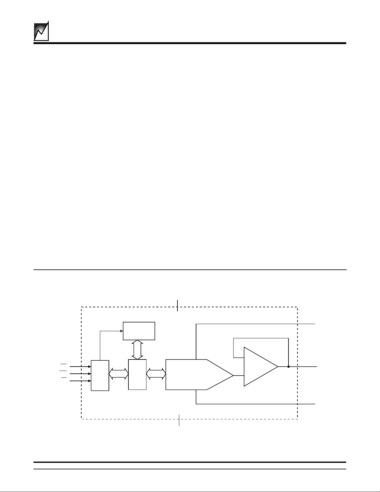
FUNCTIONAL BLOCK DIAGRAM
UP/DN
INC
CS
Counter
&
Write
Control
8-bit E2 PROM
8-bit
Data
Register
V
DD
8-bit DAC
-
+
AMP
V
V
OUT
V
H
L
GND
2016 ILL2.1
SUMMIT MICROELECTRONICS, Inc. • 300 Orchard City Drive, Suite 131 • Campbell, CA 95008 • Telephone 408-378-6461 • Fax 408-378-6586 • www.summitmicro.com
© SUMMIT MICROELECTRONICS, Inc. 1999
2016-04 4/24/99
1
Characteristics subject to change without notice

S9318
PIN NAMES
Symbol Description
INC Increment Input, High to Low
Edge Trigger
UP/DN Up/Down Input controlling relative
V
movement
OUT
V
H
V+ reference input
GND Analog and Digital Ground
V
OUT
V
L
Trimmed Voltage Output
V- reference input
CS Active low chip select input
V
DD
Supply Voltage (2.7V to 5.5V)
Analog Section
The S9318 is an 8-bit, voltage output digital-to-analog
converter (DAC). The DAC consists of a resistor network
that converts an 8-bit value into equivalent analog output
voltages in proportion to the applied reference voltage.
Reference Inputs
The voltage differential between the VL and VH inputs
sets the full-scale output voltage range. VL must be equal
to or greater than ground (i.e. a positive voltage). VH must
be greater than VL and less than or equal to VDD. See
table on page 3 for guaranteed operating limits.
Output Buffer Amplifier
The voltage output is a precision unity-gain follower that
can slew up to 1V/µs.
Digital Interface
The interface is designed to emulate a simple up/down
counter, but instead of a parallel count output, a
ratiometric voltage output is provided.
PINOUT
INC
UP/DN
V
GND
Chip Select (
1
2
3
H
4
CSCS
CS) is an active low input. Whenever CS is
CSCS
8
7
6
5
2016 ILL1.1
V
CS
V
V
DD
L
OUT
high the S9318 is in standby mode and consumes the
least power. This mode is equivalent to a potentiometer
that is adjusted to the required setting. When CS is low the
S9318 will recognize transitions on the INC input and will
move the V
either toward the VH reference or toward
OUT
the VL reference depending upon the state of the UP/DN
input.
The host may exit an adjustment routine in two ways:
deselecting the S9318 while INC is low will not perform a
store operation (a subsequent power cycle will recall the
original data); deselecting the S9318 while INC is high will
store the current V
Increment (
INCINC
INC) is an edge triggered input. Whenever
INCINC
setting into nonvolatile memory.
OUT
CS is low and a high to low transition occurs on the INC
input, the V
voltage will either move toward VH or V
OUT
depending upon the state of the UP/DN input.
UP/Down (UP/
DNDN
DN) is an input that will determine the V
DNDN
OUT
movement relative to VH and VL. When CS is low, UP/DN
is high and there is a high to low transition on INC, the
V
voltage will move (1/256th x VH-VL) toward VH.
OUT
When CS and UP/DN are low, and there is a high to low
transition on INC, the V
will move (1/256th x VH-VL)
OUT
toward VL.
L
2016-04 4/24/99
2
 Loading...