SUMMIT S39421S Datasheet
SUMMIT
MICROELECTRONICS, Inc.
Hot Swap Voltage Controller
S39421
FEATURES
• Full Voltage Control for Hot Swap Applications
– Card Insertion Detection
– Platform Voltage Detection
– Card Voltage Sequencing
– 5 Volt, 12 Volt and 3.3 Volt
• 12 Volt FET Enable Outputs
– Allows use of Low On-resistance N-Channel
FETS
• Card Reset Generation Based on Out of Spec
Voltages
– Host Reset
• Programmable Slew Rate Control [250V/Sec
Default Rate]
• Supports 5 Volt, 3.3 Volt and Mixed Voltage
Cards
• Integrated 1K Bit E
2
PROM Memory
• Data Download™ Mode [Simplifies
Downloading of Configuration Memory into
Interface ASIC or MCU]
DESCRIPTION
The S39421 is a fully integrated hot swap controller
intended for use on add-in cards that may be inserted into
or removed from powered-on host platforms. The S39421
performs a variety of tasks starting with the validation of
proper card insertion and the presence of “in-spec” voltages at the host platform interface.
Once power is switched on, the S39421 continues to
monitor the back-end power to the add-in card and the
host power supply. If either the 5V or 3.3V supplies drop
below Vtrip the S39421 will immediately assert the RESET outputs and power-down the add-in card.
In addition to the power control for the add-in card, the
S39421 provides status signals that can be employed by
the host and for the control of bus interface components.
The on board E2PROM can be used as configuration
memory for the individual card or as general purpose
memory. The proprietary DataDownload mode provides
a more direct interface to the E2PROM for simplified
access by the add-in card’s controller or ASIC.
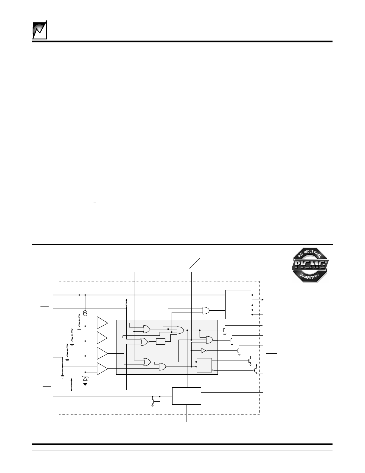
FUNCTIONAL BLOCK DIAGRAM
VCC5
PND1
+
VCC3
CARD_5V
CARD_3V
PND2
ISLEW
-
+
-
+
-
+
-
VSEL
HST_PWR
Filter
Sequencing
Logic
Slew Rate
Control
HST_RST
RESET
Timer
EEPROM
Memory
Array
DD
DO
CS
SK
DI
DRVREN
SGNL_VLD
CARD_V_VLD
RESET
RESET
VGATE3
VGATE5
ASSOCIATE
MEMBER
VCC12
© SUMMIT MICROELECTRONICS, Inc. 2001 • 300 Orchard City Drive, Suite 131 • Campbell, CA 95008 • Telephone 408-378-6461 • Fax 408-378-6586 • www.summitmicro.com
Characteristics subject to change without notice
2024 9.1 1/23/01
2024 ILL2.1
1
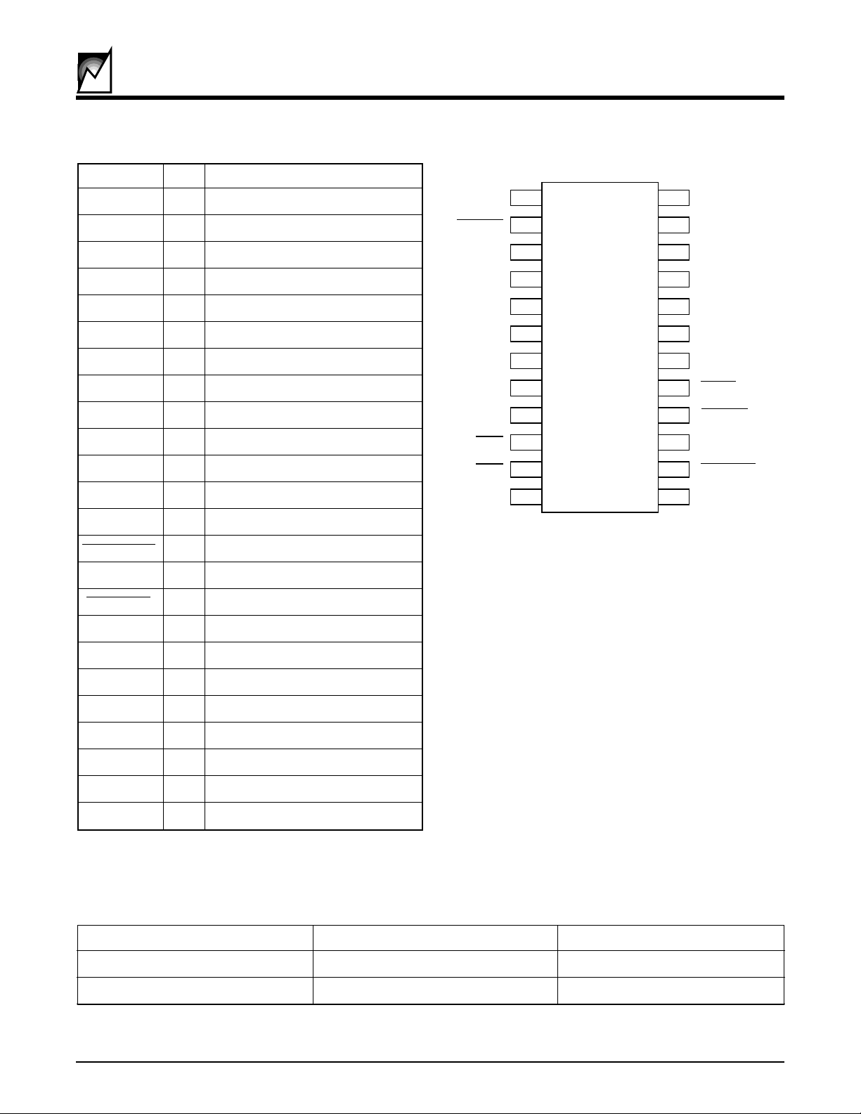
PIN CONFIGURATION
Symbol Pin Description
VCC12 1 12 Volt Input
DRVREN 2 High Side Driver Enable (L)
ISLEW 3 Slew Rate Control
VSEL 4 Voltage Select
DD 5 Data Download Enable
CS 6 Microwire Chip Select
SK 7 Microwire Serial Clock
DI 8 Microwire Data In
DO 9 Microwire Data Out
VCC12
DRVREN
ISLEW
VSEL
1
2
3
4
DD
5
CS
6
SK
7
DI
8
DO HST_RST
9
24
23
22
21
20
19
18
17
16
S39421
VCC5
VGATE5
CARD_5V
VCC3
VGATE3
CARD_3V
RESET
RESET
PND2 10 Pin Detect 2 (Active Low)
PND1 11 Pin Detect 1 (Active Low)
GND 12 Ground
CARD_V_VLD
13 Card Voltage Valid
SGNL_VLD 14 Signals Valid (Active Low)
HST_PWR 15 Host Power Up Enable
HST_RST 16 Host Reset (Active Low)
RESET 17 RESET(Active Low)
RESET 18 RESET
CARD_3V 19 Card’s 3 Volt Monitor Input
VGATE3 20 3 Volt Gate Output
VCC3 21 3 Volt Input
CARD_5V 22 Card’s 5 Volt Monitor Input
VGATE5 23 5 Volt Gate Output
VCC5 24 5 Volt Input
PND2
PND1
GND
10
11
12
15
14
CARD_V_VLD
13
HST_PWR
SGNL_VLD
2024 ILL1.1
RECOMMENDED OPERATING CONDITIONS
Condition Min Max
Temperature -40°C +85°C
V
CC
2
2.7V 5.5V
2024 9.1 1/23/01
2024 PGM T1.1
SUMMIT MICROELECTRONICS, Inc.
S39421
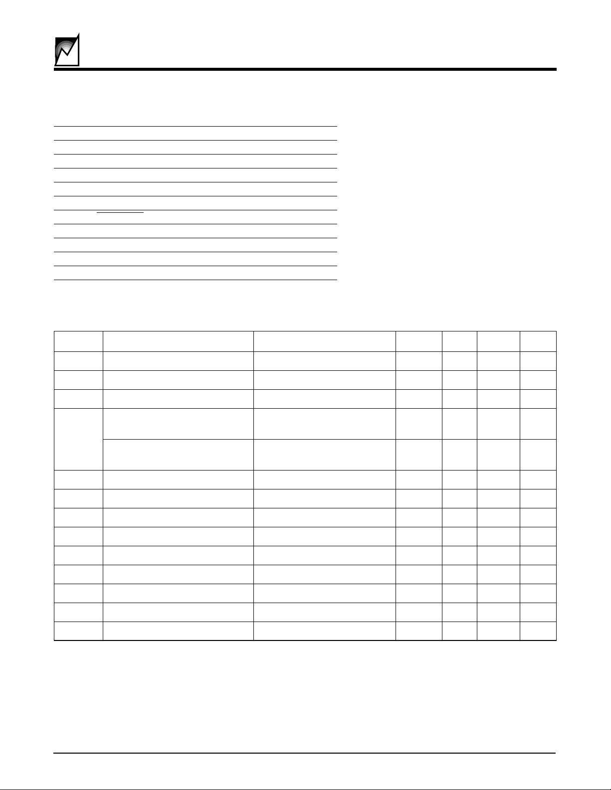
ABSOLUTE MAXIMUM RATINGS*
Temperature Under Bias -55°C to +125°C
Storage Temperature -65°C to +150°C
Voltage on :
DRVREN
VCC12 15V
VCC3 7V
CARD_5V 7V
CARD_3V 7V
SGNL_VLD, CARD_V_VLD & RESET 12V
COMMENT
Stresses listed under Absolute Maximum
Ratings may cause permanent damage to
the device. These are stress ratings only, and
functional operation of the device at these or
any other conditions outside those listed in
the operational sections of this specification
is not implied. Exposure to any absolute
maximum rating for extended periods may
affect device performance and reliability.
RESET VCC +.7V
All Others VCC +.7V
Output Short Circuit Current 100mA
Lead Solder Temperature (10 secs) 300°C
DC OPERATING CHARACTERISTICS (Over Recommended Operating Conditions)
Symbol Parameter Conditions Min Typ Max Units
I
CC1
I
CC2
Power Supply Current Resets Active, VGATES Ramping .6 1 mA
Power Supply Current
Quiesent - Resets released, VGATES On
250 500 µA
I
CC3
V
TRIP
V
TRHST
I
LI
I
LO
V
IL
V
IH
V
OL
V
OH
V
OLRS
V
OHRS
Power Supply Current Quiesent - EEPROM Access .8 1.5 mA
VTRIP Sense Levels VCC5 and CARD_5V 4.5 4.6 4.75 V
Low to High
High to Low
VCC3 and CARD_3V 2.8 2.9 3.0 V
VCC5 and CARD_5V 4.5 4.70 V
VCC3 and CARD_3V 2.8 2.95 V
Trip Point Hysteresis 7 mV
Input Leakage Current 1 2 µA
Output Leakage Current 2 10 µA
Input Low Voltage -0.1 0.8 V
Input High Voltage 2 VCC+1 V
Output Low Voltage VCC = 5.0V, IOL = 2.1mA 0.4 V
Output High Voltage VCC = 5.0V, IOH = -400µA 2.4 V
RESET Output Low Voltage IOL = 3.2mA 0.4 V
RESET Output High Voltage IOH = -800 µA VCC-.75V V
2024 PGM T2.3
SUMMIT MICROELECTRONICS, Inc.
2024 9.1 1/23/01
3
S39421
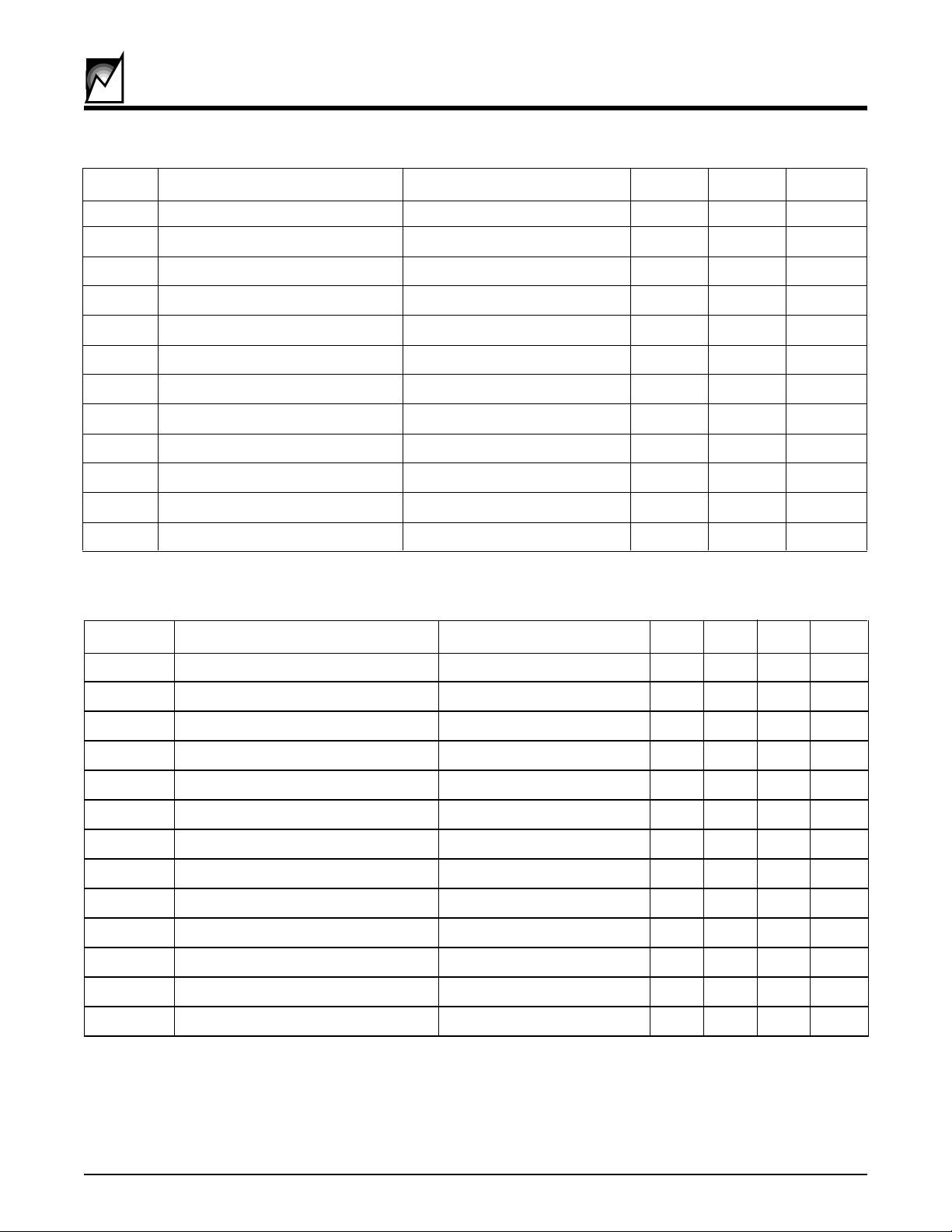
MEMORY AC OPERATING CHARACTERISTICS (Over Recommended Operating Conditions)
Symbol Parameter Conditions Min Max Units
t
CSS
CS Setup Time 50 ns
50
t
CSH
t
DIS
t
DIH
t
PD1
t
PD0
t
HZ
t
EW
t
CSMIN
t
SKHI
t
SV
SK
MAX
CS Hold Time 0 ns
DI Setup Time 100 ns
DI Hold Time 100 ns
Output Delay to 1 250 ns
Output Delay to 0 250 ns
Output Delay to Hi-Z 100 ns
Program/Erase Time 10 ms
Minimum CS Low Time 250 ns
Minimum SK Low Time 250 ns
Output Delay to Status Valid 250 ns
Maximum Clock Frequency 1 MHz
0
2024 PGM T3.1
SEQUENCER AC OPERATING CHARACTERISTICS (Over Recommended Operating Conditions)
Symbol Parameter Notes Min Typ Max Units
T
SLEW
Slew Rate 250 280 V/Sec
T
HSE
V
TRHST
t
PURST
V
RVALID
t
GLTICH
t
LVVG
t
LVSV
t
LVDE
t
RPD
t
CRVG
t
CRSV
t
CRDE
High Side Enable Delay Card Insertion Noise Filter 100 140 200 ms
Trip Point Hysteresis 7 mV
Power-up Reset Timeout 105 130 200 ms
RESET Output Valid 1 .9 V
Glitch Reject Pulse Width 40 ns
Loss of Voltage to V
off w. 100 pf load 2 µs
GATE
Loss of Voltage to Signal Valid off 5 µs
Loss of Voltage to Drive Enable off 20 µs
V
to RESET output Delay 5 µs
TRIP
Card Removal to V
off w. 100 pf load 2 µs
GATE
Card Removal to Signal Valid off 5 µs
Card Removal to Drive Enable off 20 µs
2024 PGM T4.4
4
2024 9.1 1/23/01
SUMMIT MICROELECTRONICS, Inc.
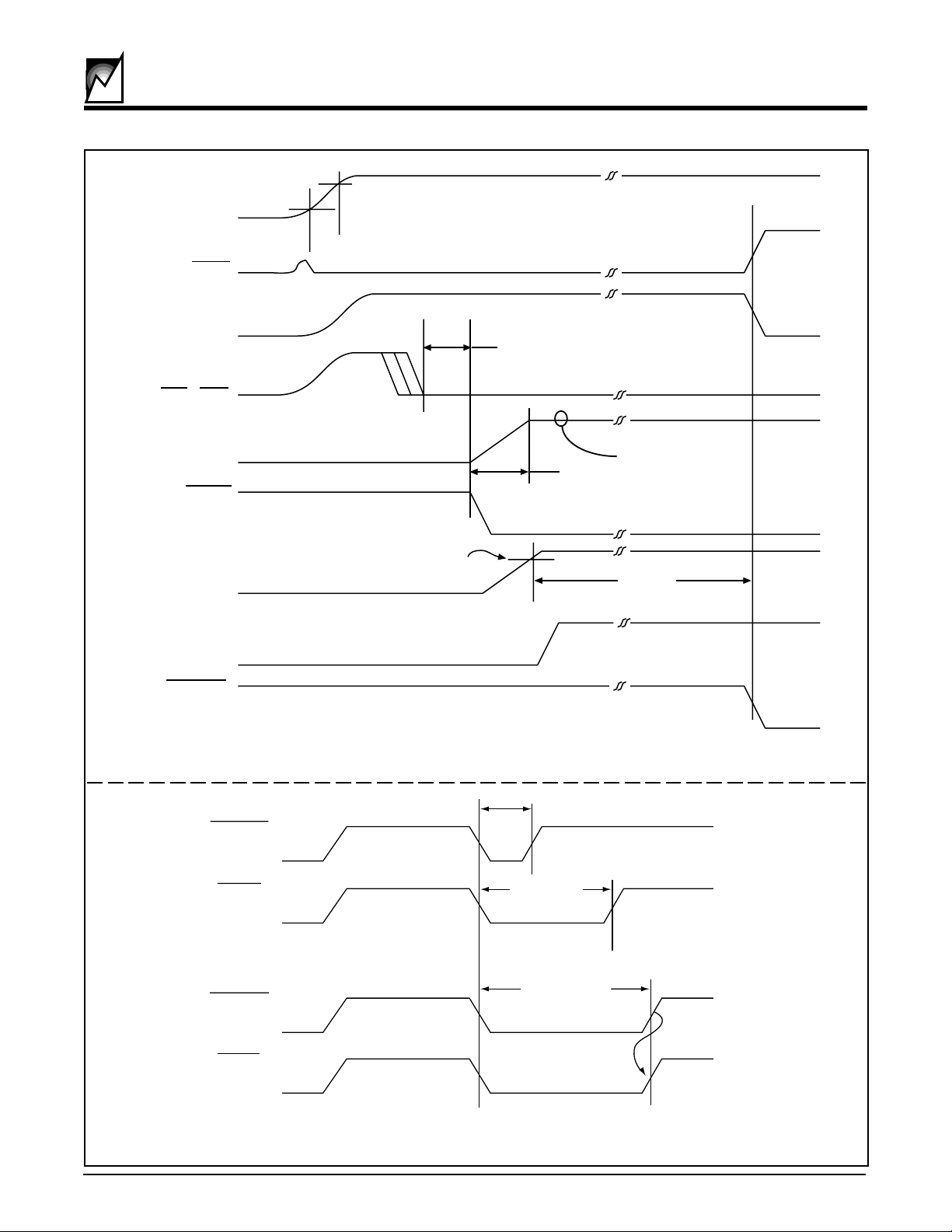
V
CC5
RESET
V
RVALID
V
TRIP5
S39421
RESET
PND1+PND2
V
CARD_5V & CARD_3V
& V
GATE5
CARD_V_VLD
SGNL_VLD
GATE3
DRVREN
V
CARD3
V
CARD5
tHSE
12V Level
tSLEW
&
tPURST
2024 ILL3.1
HST_RST
[input]
RESET
[output]
HST_RST
[input]
RESET
[output]
SUMMIT MICROELECTRONICS, Inc.
<tPURST
=tPURST
>tPURST
2024 ILL31.0
FIGURE 1. CARD INSERTION AND HOST RESET TIMING DIAGRAM
2024 9.1 1/23/01
5
VCC5
S39421
12V
VGATE5 & VGATE3
SGNLVLD
DRVEN
CARD5V
CARD_V_VLD & RESET
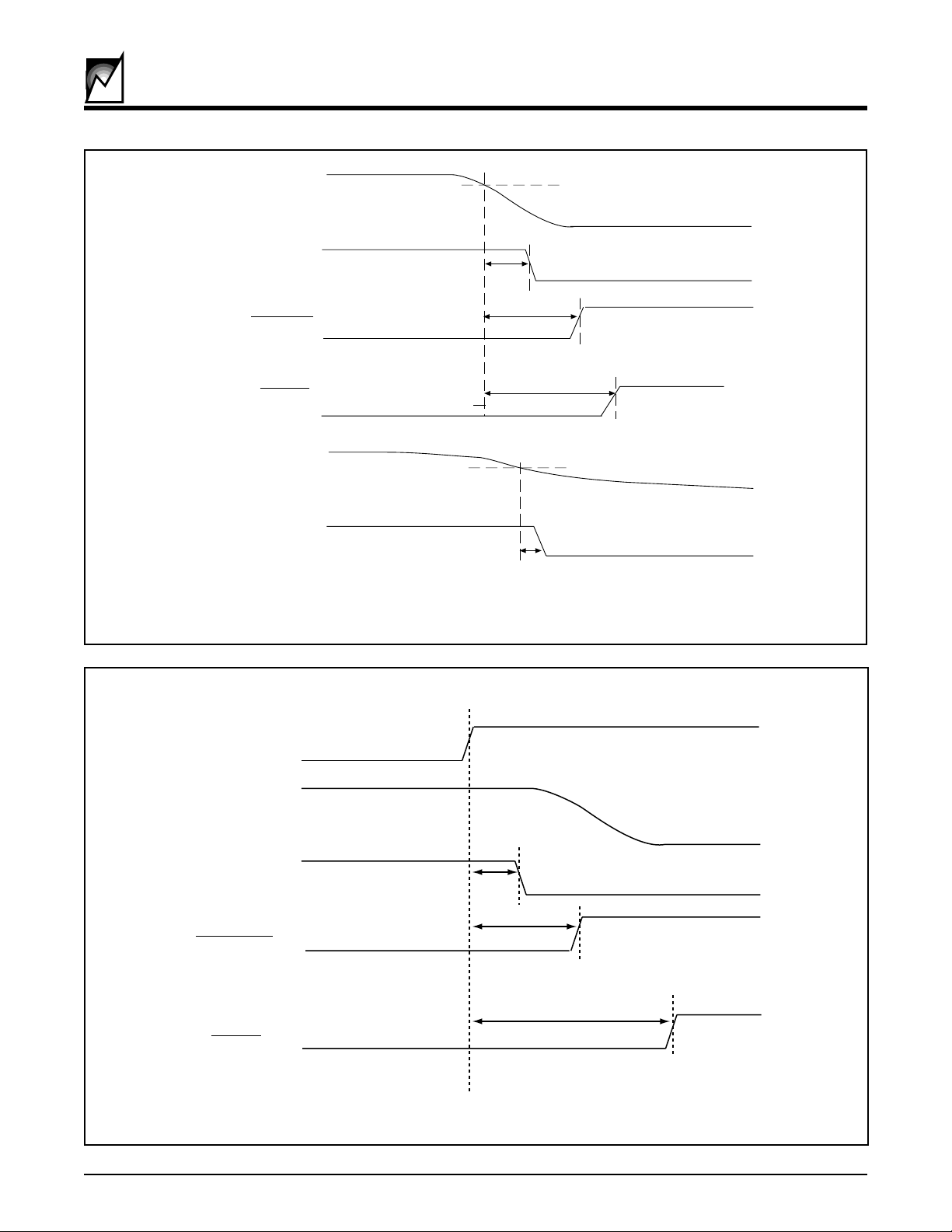
FIGURE 2. LOSS OF VOLTAGE TIMING SEQUENCE
tLVVG
tLVSV
tLVDE
tRPD
2024 ILL4.2
PinD1+PinD2
VCC5
12V
VGATE5 & VGATE3
tCRVG
tCRSV
SGNL_VLD
DRVEN
FIGURE 3. CARD REMOVAL TIMING SEQUENCE
6
tCRDE
2024 9.1 1/23/01
2024 ILL5.2
SUMMIT MICROELECTRONICS, Inc.
S39421
PIN DESCRIPTIONS
PIN NAME [
CompactPCI
name] (pin #)
VCC12 (Pin 1): Supplies the 12 volts required for power-
ing the high-side drivers.
DRVREN (Pin 2): Open drain, active low output indicates
the status of the 3 volt and 5 volt high side driver outputs
(VGATE5 and VGATE3). This signal may also be used as
a switching signal for the 12 volt supply.
ISLEW (Pin 3): Diode-connected NFET input may be
used to adjust the 250V/s default slew rate of the high-side
driver outputs. One quarter of the current injected into this
pin will be mirrored into each of the high-side driver
outputs.
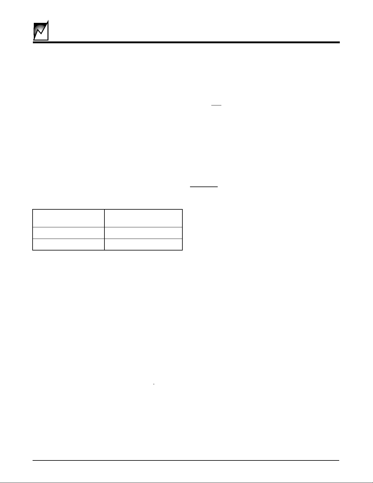
VSEL (Pin 4): TTL level input used to determine which of
the Host power supply inputs will be monitored for valid
voltage and reset generation.
VSEL-Voltage Host Voltage
Select Monitored
Low 5 Volt or Mixed-Mode
High 3.3 Volt Only
DD (Pin 5): A high going edge on this input will place the
embedded memory into Data Download mode. This
mode allows the entire contents of the E2PROM array to
be read out of the device by selecting the device (CS high)
and providing clock cycles on the SK input. Data Down-
load mode is exited when Chip Select is brought low.
CS (Pin 6): E2PROM memory chip select, active high.
SK (Pin 7): E2PROM memory serial clock input.
DI (Pin 8): E2PROM memory data input.
DO (Pin 9): E2PROM memory data output.
PND2 [BD_SEL2#] (Pin 10): Active low TTL level input
with internal pull-up to VCC5. In conjunction with PND1,
this signal indicates proper card insertion. This pin must
be connected to ground on the host side of the connector.
PND1 and PND2 must be placed on opposite corners of
the connector and will preferably be staggered shorter
than the power connector pins. Board insertion is assumed when PND1 and PND2 are low.
PND1 [BD_SEL1#] (Pin 11): Active low TTL level input
with internal pull-up to VCC5. In conjunction with PND2,
this signal indicates proper card insertion.
GND (Pin 12): Ground.
CARD_V_VLD (pin13): CARD_V_VLD is an open drain
output, indicating the card side voltages are at or above
V
.
TRIP
SGNL_VLD (Pin 14): Signals valid (SGNL_VLD) is an
open drain active low signal indicating the card side power
is valid and that the reset signals have been released.
This signal can be used by the host as an indication that
the bus interface is active and all signals are valid.
HST_PWR (pin15): The host power (HST_PWR) input is
an active high input. It provides the host system active
control over the sequencing of the power up operation.
When low, the S39421 will hold the add-in card in reset
and block all power to the backend logic. When
HST_PWR is high the power sequencing will begin immediately and the reset outputs will be driven active after
t
.
PURST
HST_RST [PCI_RST#] (Pin 16): TTL level input used as
a reset input signal from the host interface. An active low
level longer than 40 nsec will cause a reset sequence to
be performed on the card. The power switching logic will
not be affected.
RESET (Pin 17): RESET is an active low open-drain
output. It should be tied high through a pull-up resistor
connected to VCC.
RESET (Pin 18): RESET is an active high open drain
(PFET) output. It should be tied low through a pull-down
resistor connected to ground.
CARD_3V (Pin 19): 3.3 volt card side supply input. This
input is monitored for power integrity. If it falls below the
3.3V sense threshold, the PWR_VLD signal is de-asserted and a RESET sequence initiates.
VGATE3 (Pin 20): Slew rate limited high side driver
output for the 3.3V external Power FET gate.
VCC3 (Pin 21): 3.3 volt host side supply input. This input
is monitored for power integrity. If it falls below the 3.3V
sense threshold, the SGNL_VLD signal is de-asserted
and the high side drivers disabled.
CARD_5V (Pin 22): 5 volt card side supply input. This
input is monitored for power integrity. If it falls below the
5V sense threshold and the VSEL input is low, the
PWR_VLD signal is de-asserted and a RESET sequence
initiates.
VGATE5 (Pin 23): Slew rate limited high side driver
output for the 5V external Power FET gate.
VCC5 (Pin 24): Power to the S39421 and 5 volt host side
supply input. This input is monitored for power integrity. If
it falls below the 5V sense threshold and the VSEL input
is low, the SGNL_VLD signal is de-asserted and the high
side drivers disabled.
SUMMIT MICROELECTRONICS, Inc.
2024 9.1 1/23/01
7

S39421
DEVICE OPERATION
Power-Up Sequence
A sequencing operation is initiated by the physical insertion of the card into the platform’s connector. The
S39421’s VCC5 pin should be connected to the early
power pins of the connector. As soon as power is applied,
the S39421 will drive the reset outputs active and clamp
the VGATE outputs to ground.
Proper card insertion is insured by detecting the presence
of a low level on the pin detect (PND1, PND2) inputs,
which should be located on opposite ends of the bus
connector. These pin detect inputs have internal pull-up
resistors and the connection on the host platform side
must be connected directly to ground. [In a
CompactPCI
application these are the BD_SEL# signals]. The PND
inputs have an internal noise filter nominally set at 150ms.
Once the proper card insertion has been detected, the
S39421 will check the status of the HST_PWR signal from
the host.
Implementation of HST_PWR is optional; e.g. it can be
used to power down individual cards on the bus via
software control. If it is not used by the host system the
input must be held high in order for the S39421 to enable
power sequencing to the card.
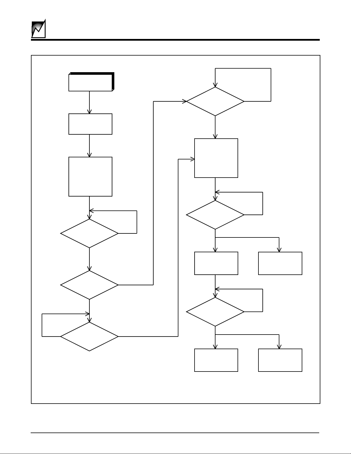
Once these basic conditions are met the S39421 will
begin the power-up portion of the sequence. First, the
host platform supplies are checked for compliance.
Based on the state of the VSEL input the S39421 will
monitor the +5V and +3.3V supplies. If these are above
the VTRIP thresholds the sequencing next begins the
backend logic power-on operation.
The S39421 will drive the VGATE3 and VGATE5 outputs
to the 12V rail to turn on the external 3 volt and 5 volt power
FETs. The slew rate of these outputs defaults to 250V/s.
Different slew rates can be accommodated by either
adding an additional capacitor between the FET gate and
ground or by injecting current into the ISLEW input.
RESET CONTROL
In order to provide positive control to an add-in-card’s
bakckend logic, the reset control function of the S39421
begins operation as soon as a voltage is applied to VCC5.
The conditions that affect the reset outputs are the VCC5,
VCC3, CARD_5V and CARD_3V input levels and the
state of the HST_RST input.
Assume HST_RST has been released and is pulled high.
The S39421 reset ouputs will be valid as long as VCC5
is • 1V. If any one of VCC5, VCC3, CARD_5V or
CARD_3V input levels is below its respective Vtrip level
the reset outputs and CARD_V_VLD output will be driven
active. (In the case of the CARD_V_VLD output, the
active condition is low but its logical true condition is a
release of its open drain output pulled high by an external
pull-up) As soon as the VCC5, VCC3, CARD_5V and
CARD_3V inputs are above their Vtrip levels
CARD_V_VLD will be released and the internal tPURST
timer will be started. The reset outputs will be held active
until tPURST has expired and then be released.
The HST_RST input is also used to control the reset
outputs. A high to low transition on HST_RST will initiate
a reset cycle with a duration of tPURST. The reset outputs
will remain active for a minimum period tPURST or for the
duration of HST_RST active low, whichever is longer. A
HST_RST activated reset will not affect the power sequencing logic.
During normal operation, the supply voltages are continuously monitored. If the cardside supplies fall below the
VTRIP levels the reset outputs will be driven active. If the
host platform supplies fall below VTRIP, the S39421 will
immediately assert the reset outputs and disable the
highside drivers.
Power Configurations
The S39421 can be used in 5V-only, 3.3V-only and mixed
voltage systems. For mixed voltage systems, simply
connect the appropriate bus and card power inputs as
indicated. The VSEL pin should be grounded.
For systems with a single power supply, connect VCC5
and VCC3 together to the platform host early power line
(long pin power supply). Also connect CARD5V and
CARD3V together to the cardside power output of the
FET.
The state of VSEL determines the reset level that will be
used to signal CARD_V_VLD. For 3.3V systems, tie
VSEL to the supply; for 5V systems, tie VSEL to ground.
8
2024 9.1 1/23/01
SUMMIT MICROELECTRONICS, Inc.
VCC5 ≥ 1V
S39421
ASSERT
RESET
OUTPUTS
SHUT OFF
VGTE5
VGTE3
DRVREN
PWR_VLD
SGNL-VLD
PND1
&
PND2?
YES
VSEL
HI ?
NO
NO
HOST
5V & 3V
OK?
YES
TURN-ON
VGTE5
VGTE3
DRVREN
CARD 5V & 3V
OK?
YES
START
RESET
TIMER
NO
NO
TURN ON
PWR_VLD
NO
3VOLT
OK?
SUMMIT MICROELECTRONICS, Inc.
YES
YES
FIGURE 4.
2024 9.1 1/23/01
tPURST
TIMEOUT?
YESHOST
RELEASE
RESETS
NO
TURN ON
SGNL_VLD
2024 ILL6.2
9
