

Page 1

SIS Documentation SIS3820
VME Scaler
Page 1 of 79
SIS3820
VME Scaler
User Manual
SIS GmbH
Harksheider Str. 102A
22399 Hamburg
Germany
Phone: ++49 (0) 40 60 87 305 0
Fax: ++49 (0) 40 60 87 305 20
email: [email protected]
http://www.struck.de
Version: sis3820-M-0-001-v184-scaler.doc as of 27.07.07
Page 2
SIS Documentation SIS3820
VME Scaler
Page 2 of 79
Revision Table:
Revision Date Modification
0.0x 13.02.02 Start of module definition
0.10 23.06.03 Prerelease
1.00 24.06.03 First official release
1.01 11.08.03 Id. reg R/W -> R only
bug fix in JTAG JP570 text and watchdog enable
1.10 09.12.03 VME JTAG firmware upgrade support,
read during preset scaler operation, support for 512 MB
memory strips and add mode
(Xilinx Firmware: sis38200102.mcs)
1.20 27.04.04 Firmware Version 01 03
Chained Block Transfer (CBLT) implemented
(Xilinx Firmware: sis38200103.mcs)
1.30 04.06.04 Firmware Version 01 04
48-bit deep counter implementation in channels 1 and 17
(for scaler mode, new address 0x210)
1.31 09.11.04 Bug fix in address map, change FIFO threshold register
explanation
1.32 13.01.05 Couple of index entries added, typo fix
1.40 20.05.05 Firmware Version 01 05
New Control Output mode 2 (10Mhz)
1.50 26.08.05 Firmware Version 01 08
New Control Input mode 6 (with external counter clear)
1.60 14.10.05 Firmware Version 01 09
Bug fix in control input inversion
New register 0x214 (veto external count inhibit)
1.61 20.10.05 Bug fix in example veto external count register
1.70 03.11.05 Firmware Version 01 0A
New register 0x218 (test pulse mask register)
1.71 04.12.05 Bug fixes
1.72 11.02.06 ESD note added
1.80 15.06.06 New MUX_OUT feature, firmware revision 0xB
1.81 19.06.06 Bug fixes
1.82 25.10.06 Note on external LNE/channel N rate being limited to 5
MHz
1.83 21.11.06 JTAG jumper JP570 factory default
1.84 27.07.07 50 Ω TTL and high impedance input configuration
Page 3

SIS Documentation SIS3820
VME Scaler
Page 3 of 79
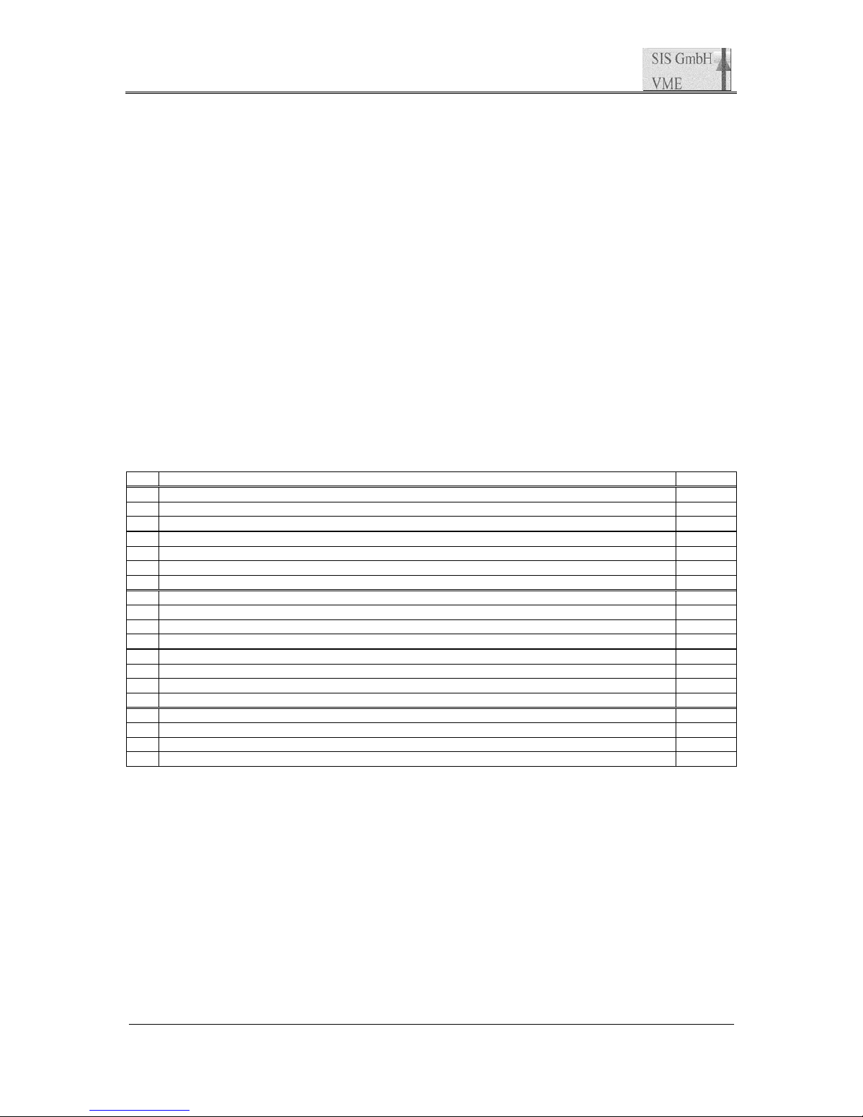
1 Table of contents
1 Table of contents ................................................................................................................. 3
2 Introduction ......................................................................................................................... 7
3 Technical Properties/Features.............................................................................................. 8
4 Functionality........................................................................................................................ 9
4.1 Block Diagram ........................................................................................................................................ 9
4.2 Modes of operation ............................................................................................................................... 10
4.2.1 Scaler/Counter............................................................................................................................... 10
4.2.2 Latching Scaler.............................................................................................................................. 10
4.2.3 Preset Scaler.................................................................................................................................. 10
4.2.4 Multi channel Scaler (MCS) ........................................................................................................ 10
4.2.5 Histogramming Scaler(3820 01 02 and higher design)................................................................. 10
5 Getting started.................................................................................................................... 11
5.1 Installation............................................................................................................................................. 11
5.2 LINUX example/test code..................................................................................................................... 11
5.2.1 User LED test................................................................................................................................ 11
5.2.2 Readout of Module Id. and firmware revision register ................................................................. 11
5.2.3 Standard Counter........................................................................................................................... 12
5.2.4 Multiscaler (MCS) ........................................................................................................................ 13
5.2.5 Preset Scaler.................................................................................................................................. 14
5.3 Win2K/XP Visual C++ example/test code............................................................................................ 15
6 VME Addressing............................................................................................................... 16
6.1 Address map.......................................................................................................................................... 17
7 Register description........................................................................................................... 18
7.1 Control/Status Register(0x, write/read)................................................................................................. 19
7.1.1 Counter test mode ......................................................................................................................... 20
7.1.2 25 MHz test pulse mode................................................................................................................ 20
7.1.3 Reference pulser channel 1 ........................................................................................................... 20
7.2 Module Id. and Firmware Revision Register (0x4, read)...................................................................... 21
7.2.1 Major revision numbers ................................................................................................................ 21
7.3 Interrupt configuration register (0x8).................................................................................................... 22
7.3.1 IRQ mode...................................................................................................................................... 22
7.4 Interrupt Control/Status register (0xC).................................................................................................. 23
7.4.1 Interrupt sources............................................................................................................................ 24
7.5 (0x10)Acquisition preset register.......................................................................................................... 26
7.6 Acquisition count register (0x14).......................................................................................................... 26
7.7 LNE Prescaler factor register (0x18)..................................................................................................... 27
7.8 Preset value register counter group 1 (0x20)......................................................................................... 28
7.9 Preset value register counter group 2 (0x24)......................................................................................... 28
7.10 Preset Enable and Hit register (0x28).................................................................................................... 28
7.11 CBLT/Broadcast setup register............................................................................................................. 29
7.12 SDRAM page register (0x34) ............................................................................................................... 30
7.13 FIFO word counter/memory address pointer register (0x38)................................................................ 31
7.14 FIFO word counter threshold (0x3C).................................................................................................... 32
7.15 HISCAL_START_PRESET register (0x40)......................................................................................... 33
7.16 HISCAL_START_COUNTER register (0x44) .................................................................................... 33
7.17 HISCAL_LAST_ACQ_COUNTER register (0x48)............................................................................. 33
7.18 (Acquisition) Operation Mode register (0x100).................................................................................... 34
7.18.1 Modes of Operation modes (Bits 30:28) ....................................................................................... 34
7.18.2 Input modes (Bits 18:16)............................................................................................................... 35
7.18.3 Output mode (Bits 21:20).............................................................................................................. 36
7.18.4 HISCAL_START_SOURCE_BIT (Bit 14) .................................................................................. 36
7.18.5 SDRAM mode (Bit 12) and SDRAM add mode (Bit 13) ............................................................. 37
7.18.6 Arm/enable source ........................................................................................................................ 37
7.18.7 LNE source ................................................................................................................................... 38
7.18.8 Data format ................................................................................................................................... 39
Page 4

SIS Documentation SIS3820
VME Scaler
Page 4 of 79
7.18.9 Clearing/non clearing .................................................................................................................... 39
7.19 Copy disable register (0x104)............................................................................................................... 40
7.20 LNE channel select register (0x108) ..................................................................................................... 41
7.21 PRESET channel select register (0x10C).............................................................................................. 42
7.21.1 Preset scheme................................................................................................................................ 42
7.22 MUX OUT channel select register (0x110) .......................................................................................... 43
7.23 Inhibit/count disable register (0x200) ................................................................................................... 44
7.24 Counter clear register (0x204)............................................................................................................... 44
7.25 Counter Overflow register (0x208) ....................................................................................................... 44
7.26 Channel 1/17 Bits 33-48 register (0x210)............................................................................................. 45
7.27 Veto external count inhibit register (0x214) ......................................................................................... 45
7.28 Test pulse mask register (0x218) ......................................................................................................... 46
7.29 SDRAM SPD register (0x300).............................................................................................................. 46
7.30 JTAG_TEST register ............................................................................................................................ 47
7.31 JTAG_DATA_IN register..................................................................................................................... 47
7.32 JTAG_CONTROL register ................................................................................................................... 47
7.33 One wire Id. register (tbd)..................................................................................................................... 48
7.34 FIFO address space (0x800000-0xFFFFFC)......................................................................................... 49
7.34.1 non incrementing VME master .....................................................................................................49
7.34.2 incrementing VME master ............................................................................................................ 49
7.35 SDRAM address space (0x800000-0xFFFFFC) ................................................................................... 49
8 Data Format ....................................................................................................................... 50
8.1 32-bit Mode........................................................................................................................................... 50
8.2 24-bit Mode........................................................................................................................................... 50
8.3 16-bit Mode........................................................................................................................................... 51
8.4 8-bit Mode............................................................................................................................................. 51
9 Front panel elements.......................................................................................................... 52
9.1 Front Panel Layout................................................................................................................................ 52
9.2 Front Panel LEDs.................................................................................................................................. 53
9.3 Flat cable Input/Output Pin Assignments.............................................................................................. 54
9.3.1 ECL ............................................................................................................................................... 54
9.3.2 TTL ............................................................................................................................................... 55
10 Board Layout.................................................................................................................. 56
11 Jumper settings/pinouts.................................................................................................. 57
11.1 J1........................................................................................................................................................... 57
11.2 J90......................................................................................................................................................... 57
11.3 JP570 JTAG source............................................................................................................................... 58
11.4 CON500 JTAG ..................................................................................................................................... 58
12 Input Configuration ........................................................................................................ 59
12.1 ECL....................................................................................................................................................... 59
12.2 LVDS.................................................................................................................................................... 60
12.3 NIM....................................................................................................................................................... 61
12.4 TTL ....................................................................................................................................................... 62
12.4.1 High impedance TTL/LEMO........................................................................................................ 62
12.4.2 50Ω TTL/LEMO........................................................................................................................... 62
12.4.3 TTL/Flat Cable.............................................................................................................................. 62
13 TTL output configuration ............................................................................................... 63
14 Signal Specification........................................................................................................ 63
14.1 Control Signals...................................................................................................................................... 63
14.2 Inputs..................................................................................................................................................... 63
14.3 User Bits................................................................................................................................................ 63
15 Theory of operation ........................................................................................................ 64
15.1 Enable Logic......................................................................................................................................... 64
15.2 Read on the fly...................................................................................................................................... 65
15.3 Latching scaler...................................................................................................................................... 65
15.4 Preset Scaling........................................................................................................................................ 65
15.5 Multiscaling (MCS) .............................................................................................................................. 66
15.5.1 Minimum dwell time..................................................................................................................... 66
Page 5

SIS Documentation SIS3820
VME Scaler
Page 5 of 79
15.5.2 arm/enable with MCS.................................................................................................................... 67
15.6 Clearing/non clearing mode .................................................................................................................. 67
15.7 Histogramming Scaler (HISCAL)......................................................................................................... 68
15.7.1 Minimum dwell time in HISCAL mode........................................................................................ 68
15.8 Firmware upgrade over VME ............................................................................................................... 68
15.9 CBLT readout (3820 01 03 and higher design)....................................................................................69
15.9.1 CBLT Setup example.................................................................................................................... 70
15.9.2 CBLT hints.................................................................................................................................... 71
15.10 Broadcast........................................................................................................................................... 71
16 Appendix ........................................................................................................................ 72
16.1 P2 row A/C pin assignments ................................................................................................................. 72
16.2 Row d and z Pin Assignments............................................................................................................... 73
16.3 Connector Types ................................................................................................................................... 74
16.4 Power consumption............................................................................................................................... 74
16.5 Operating conditions............................................................................................................................. 74
16.5.1 Cooling.......................................................................................................................................... 74
16.5.2 Hot swap/live insertion.................................................................................................................. 74
16.6 LED (selftest)........................................................................................................................................ 74
16.7 VME readout performance.................................................................................................................... 75
16.8 Software Support................................................................................................................................... 75
17 Glossary.......................................................................................................................... 76
18 Index............................................................................................................................... 77
Page 6

SIS Documentation SIS3820
VME Scaler
Page 6 of 79
Page 7
SIS Documentation SIS3820
VME Scaler
Page 7 of 79
2 Introduction
The SIS3820 is a multi purpose counter. It combines the functionality of the SIS3800 scaler
and the SIS3801 multiscaler with extended functions. The proven concept of flexible leaded
component based frontend circuitry in conjunction with more recent FPGA (field
programmable gate array) technology results in unprecedented flexibility to implement the
given readout application.
Applications comprise, but are not limited to:
• Nuclear Phyics
• Particle Physics
• Neutrino/Astrophysics
• Synchrotron Radiation
• Neutron Scattering
• Machine (accelerator) diagnosis
• Scanning microscope readout
Page 8

SIS Documentation SIS3820
VME Scaler
Page 8 of 79
3 Technical Properties/Features
This manual describes the implemented functionality for the SIS3820-SCALER firmware.
Other firmware designs are SIS3820-CLOCK (clock distributor for up to 32 SIS330x VE
digitizers) and SIS3820-LATCH (input register with counter and interrupt functionality)
Find below a list of key features of the SIS3820.
• 32 channels (64 channel option)
• 4 front panel control inputs
• 4 front panel control outputs
• 64 Mbytes SDRAM (512 MB option)
• 250 MHz counting rate (ECL and NIM), 100 MHz for TTL (50 MHz for P2 fed channels)
• 32-bit counter depth (channel 1 and 17 48-bit deep with firmware > 01 04 in scaler mode)
• NIM/TTL/ECL/LVDS versions
• flat cable (ECL, TTL and LVDS) and LEMO (TTL/NIM) options
• multi channel, latching and preset scaler operation
• shadow register (latching scaler mode)
• read on the fly (latching scaler mode)
• reference pulser
• test pulser
• A24/32 D32/BLT32/MBLT64/2eVME/CBLT32)
• Geographical addressing mode (in conjunction with VME64x backplane)
• Broadcast addressing
• Interrupt capabilities
• Hot swap (in conjunction with VME64x backplane)
• VME64x Connectors
• VME64x Side Shielding
• VME64x Front panel
• VME64x extractor handles (on request)
• single supply (+5 V)
• in field firmware upgrade capability
Page 9
SIS Documentation SIS3820
VME Scaler
Page 9 of 79
4 Functionality
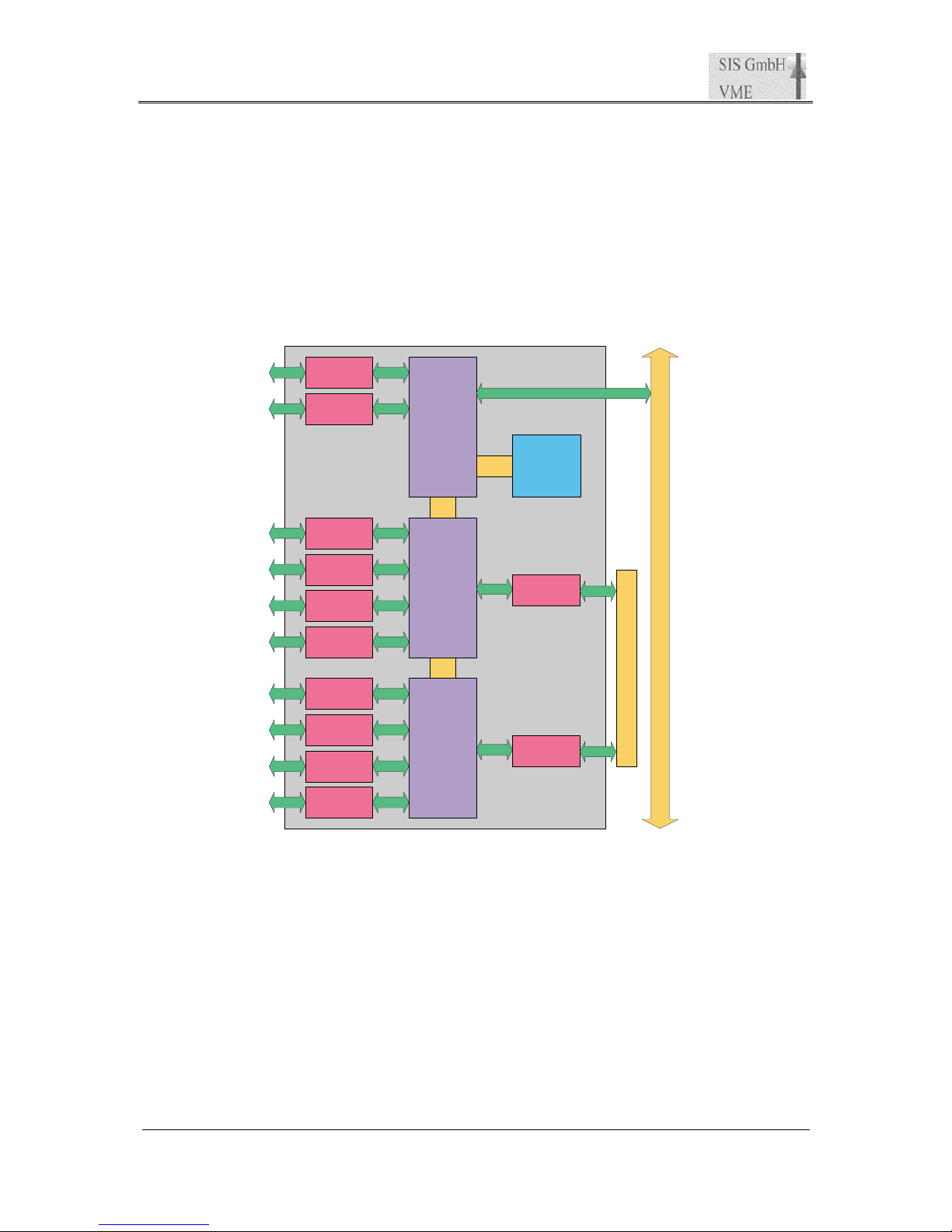
The functionality of the SIS3820 is a combination of hardware (printed circuit board) design,
stuffing options and firmware. The module consists of two FPGAs that hold the frontend
logic and on FPGA that holds the VME interface, the SDRAM controller and the control logic
functions. Logic level adaptation is handled by classic DIL components and single inline
(SIL) resistor networks. The firmware is loaded from a serial PROM at power up. Both JTAG
and VME can be used for in field firmware upgrades/changes.
4.1 Block Diagram
SDRAM
4 x
Level Adaptation
Driver/Receiver
4 x
Level Adaptation
Driver/Receiver
4 x
Level Adaptation
Driver/Receiver
4 x
Level Adaptation
Driver/Receiver
Driver/Receiver
16 x
Frontend
FPGA
4 x
Level Adaptation
Driver/Receiver
4 x
Level Adaptation
Driver/Receiver
4 x
Level Adaptation
Driver/Receiver
4 x
Level Adaptation
Driver/Receiver
Driver/Receiver
16 x
VME
and
Control
FPGA
4 x
Level Adaptation
Driver/Receiver
4 x
Level Adaptation
Driver/Receiver
Frontend
FPGA
P2 (A,C)
VME P1 and P2
Page 10

SIS Documentation SIS3820
VME Scaler
Page 10 of 79
4.2 Modes of operation
4.2.1 Scaler/Counter
In standard counter/scaler mode data can be read on the fly with an accuracy to the least
significant bit. No counts are lost in read on the fly mode.
4.2.2 Latching Scaler
In latching scaler mode scaler values are copied to a shadow register set upon a front panel
signal LNE or a VME command. Broadcast functionality is implemented for the later to allow
for minimum time difference over a set of several SIS3820s without front panel cabling.
4.2.3 Preset Scaler
The SIS3820 can be operated as preset scaler. An arbitrary channel or a combination of
channels can be selected as the condition for the termination of the counting process. The
selection of the channel(s) is done via the preset enable mask register . The first selected
channel that reaches its preset value will terminate the counting process. The actual preset
values are defined though the preset value register set. The internal 25 MHz pulse generator
(or a prescaled derived output) can be used as time base for measurements if its enabled for
channel 1 with this channel being enabled in the preset enable mask and the desired prescale
factor stored into the channel 1 preset value register. The terminating channel can be
identified by the actual scaler data or the preset hit mask register if more than one preset
channel is enabled.
4.2.4 Multi channel Scaler (MCS)
MCS mode allows for the buffered readout of variable or fixed lengths counting time
intervals. The interval length can be defined by an internal timer as well as by an external
signal, which can be prescaled also. The minimum buffer memory size of 64 MB takes the
realtime burden away from the VME master even at very short time intervals (dwell times).
Two factors facilitate short dwell time applications. The first is high speed VME readout of
data from SDRAM in MBLT64 and 2eVME. The second is data compression with a
reduction in counter depth to 16 or 8-bit. Data compression is also a good way to save VME
bandwidth in lower count rate applications (with V/F converters e.g.) at longer dwell times.
4.2.5 Histogramming Scaler(3820 01 02 and higher design)
Histogramming scaler mode (MCS mode with add enabled) allows to acquire and add MCS
data of several repeated scans in SDRAM without CPU interaction. The user has to make
sure, that the reset to the first bin and the number of bins are issued with the accuracy that is
required by the application. I.e. no number of bin/reset checking mechanism is implemented
(unlike in the SIS3100-HISCAL DSP based design).
Page 11

SIS Documentation SIS3820
VME Scaler
Page 11 of 79
5 Getting started
This section is intended for the first time SIS3820 user. In some cases it may be good enough
to use the provided header file and C examples to get acquainted to a couple of the modules
functions before looking at the other sections of the manual in more detail. If you have a
SIS1100/3100 PCI to VME interface under LINUX or under Win2K/XP with Visual C++ you
can use the provided example code without modifications.
5.1 Installation
• Select addressing A32 or geographical address mode with J1 (factory default is A32)
• Select base address with SW3 and SW4 in non geographical addressing (the default base
address setting is 0x38000000)
• turn VME crate power off
• install your SIS3820 board in the VME crate
• connect inputs
• turn VME crate power back on
• verify, that the P (power) and R (ready) LEDs are on and all other LEDs are off after the
approximately 2s long power up self test cycle
5.2 LINUX example/test code
The file sis3820.tar.gz holds LINUX example programs, the sis3820.h header files and
Makefiles to generate the executables.
Initial VME access test
Both the user LED and readout of the Module Id. and firmware register provide a good way to
verify that proper initial communciation with the SIS3820 can be established.
5.2.1 User LED test
The program sis3820_led.c runs 30 cycles with the sequence user LED on, sleep(1), user LED
off, sleep(1).
5.2.2 Readout of Module Id. and firmware revision register
The program sis3820_readmodid.c reads and displays the module identification and firmware
register.
mki@mki:~/sis1100/sis3820> ./sis3820_readmodid
Module identification and firmware register reads: 38200102
Page 12

SIS Documentation SIS3820
VME Scaler
Page 12 of 79
5.2.3 Standard Counter
In the minimum counter application you enable the logic, have the module count for a period
of time and read out the scaler values after disabling the logic.
The sis3820_counter program runs 2 counting cycles of 5 s each. During the second cycle the
internal 50 MHz reference pulse generator is routed to channel 1. Sample output with a 11
MHz signal connected to scaler channel 17 is shown below.
mki@mki:~/sis1100/sis3820> ./sis3820_counter
SIS3820 scaler counting
gotwords 32
scaler data
ch01 00000000 ch02 00000000 ch03 00000000 ch04 00000000
ch05 00000000 ch06 00000000 ch07 00000000 ch08 00000000
ch09 00000000 ch10 00000000 ch11 00000000 ch12 00000000
ch13 00000000 ch14 00000000 ch15 00000000 ch16 00000000
ch17 03477ce7 ch18 00000000 ch19 00000000 ch20 00000000
ch21 00000000 ch22 00000000 ch23 00000000 ch24 00000000
ch25 00000000 ch26 00000000 ch27 00000000 ch28 00000000
ch29 00000000 ch30 00000000 ch31 00000000 ch32 00000000
now with reference pulser on ch1 enabled
SIS3820 scaler counting
gotwords 32
scaler data
ch01 0eedfb33 ch02 00000000 ch03 00000000 ch04 00000000
ch05 00000000 ch06 00000000 ch07 00000000 ch08 00000000
ch09 00000000 ch10 00000000 ch11 00000000 ch12 00000000
ch13 00000000 ch14 00000000 ch15 00000000 ch16 00000000
ch17 0348d70d ch18 00000000 ch19 00000000 ch20 00000000
ch21 00000000 ch22 00000000 ch23 00000000 ch24 00000000
ch25 00000000 ch26 00000000 ch27 00000000 ch28 00000000
ch29 00000000 ch30 00000000 ch31 00000000 ch32 00000000
Note: The 50 MHz reference pulse generator will give you an idea on the sleep/scheduling
accuracy of your LINUX system.
Page 13

SIS Documentation SIS3820
VME Scaler
Page 13 of 79
5.2.4 Multiscaler (MCS)
MCS mode is demonstrated with the program sis3820_mcs.c. With respect to the fact that
SDRAM mode with a fixed number of acquisitions is used, its kind of a minimum approach
that does not make use of the full capabilities of the SIS3820.
The example uses the internal 10 MHz LNE source, which is run through the LNE prescaler
to minimize the need for external signals. The number of acquisitions is preset with the
acquisition preset register. The acquisition count register is used to determine completion of
the acquisition process.
Find below the output of the program for 11 LNEs (corresponding to 11 time slices) with an
input rate of 11 MHz moved across scaler channel 1 to channel 4 as the MCS acquisition is
going on. Note that the CLR LED is pulsed with every LNE and that the S LED is on from
the enable command until the acquisition preset has been reached.
mki@mki:~/sis1100/sis3820> ./sis3820_mcs
MCS mode, scan 1 completed
MCS mode, scan 2 completed
MCS mode, scan 3 completed
MCS mode, scan 4 completed
MCS mode, scan 5 completed
MCS mode, scan 6 completed
MCS mode, scan 7 completed
MCS mode, scan 8 completed
MCS mode, scan 9 completed
MCS mode, scan 10 completed
gotwords 40
scaler data
scan: 001 ch01 00a7d8f7 ch02 00000000 ch03 00000000 ch04 00000000
scan: 002 ch01 00a7d8f7 ch02 00000000 ch03 00000000 ch04 00000000
scan: 003 ch01 008f5010 ch02 00000000 ch03 00000000 ch04 00000000
scan: 004 ch01 00000000 ch02 003d3c9f ch03 00000000 ch04 00000000
scan: 005 ch01 00000000 ch02 00a7d8f7 ch03 00000000 ch04 00000000
scan: 006 ch01 00000000 ch02 002255a6 ch03 00000000 ch04 00000000
scan: 007 ch01 00000000 ch02 00000000 ch03 006ee942 ch04 00000000
scan: 008 ch01 00000000 ch02 00000000 ch03 0076e9f4 ch04 00000000
scan: 009 ch01 00000000 ch02 00000000 ch03 00000000 ch04 00438a6e
scan: 010 ch01 00000000 ch02 00000000 ch03 00000000 ch04 00a7d8f7
Page 14

SIS Documentation SIS3820
VME Scaler
Page 14 of 79
5.2.5 Preset Scaler
The sis3820_preset example illustrates preset scaling. Counter group 1 is activated for preset
scaling with channel 4 selected as preset channel (channel 1 with the TESTMKI compiler flag
set). A value of 0x1000000 is written to the preset value register of counter group 1 and the
logic enabled afterwards. The status of the preset enable and hit register is polled until
channel group 1 has reached its preset value..
mki@mki:~/sis1100/sis3820> ./sis3820_preset
gotwords 32
scaler data
ch01 00000000 ch02 00000000 ch03 00000000 ch04 01000002
ch05 00000000 ch06 00000000 ch07 00000000 ch08 00000000
ch09 00000000 ch10 00000000 ch11 00000000 ch12 00000000
ch13 00000000 ch14 00000000 ch15 00000000 ch16 00000000
ch17 00000000 ch18 00000000 ch19 00000000 ch20 00000000
ch21 00000000 ch22 00000000 ch23 00000000 ch24 00000000
ch25 00000000 ch26 00000000 ch27 00000000 ch28 00000000
ch29 00000000 ch30 00000000 ch31 00000000 ch32 00000000
mki@mki:~/sis1100/sis3820>
Note 1: It will take in the order of 100 ns after the preset condition was detected before the
counter will stop counting. This implies, that the actual stored counter value will be greater
than the preset value for frequencies in excess of some 10 MHz. Above output was generated
with a symmetric 15 MHz source e.g.
Note 2: The current version of the sis3820_preset features readout in 1s intervals in
parallel to ongoing acquisition.
Page 15
SIS Documentation SIS3820
VME Scaler
Page 15 of 79
5.3 Win2K/XP Visual C++ example/test code
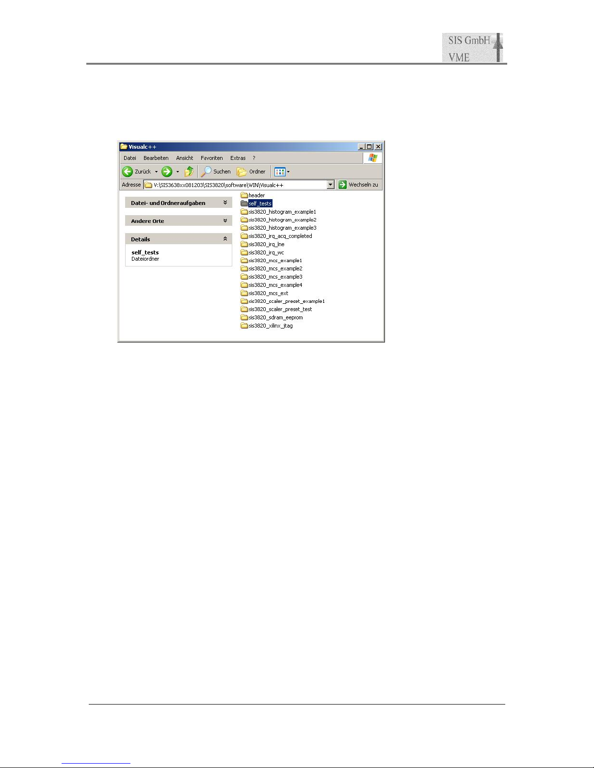
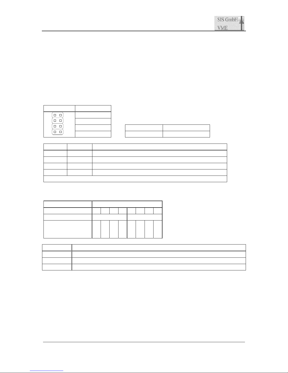
Find below a screen shot of the Visual C++ directory of the SIS36/38xx CDROM. A short
description is given in the header section of the individual C files.
Page 16
SIS Documentation SIS3820
VME Scaler
Page 16 of 79
6 VME Addressing
As the SIS3820 features memory options with up 512 Mbytes of SDRAM, A32 addressing
was implemented as the only option. Hence the module occupies an address space of
0xFFFFFF Bytes (i.e. 16 MBytes).
The SIS3820 firmware addressing concept is a pragmatic approach to combine standard
rotary switch style settings with the use of VME64x backplane geographical addressing
functionality.
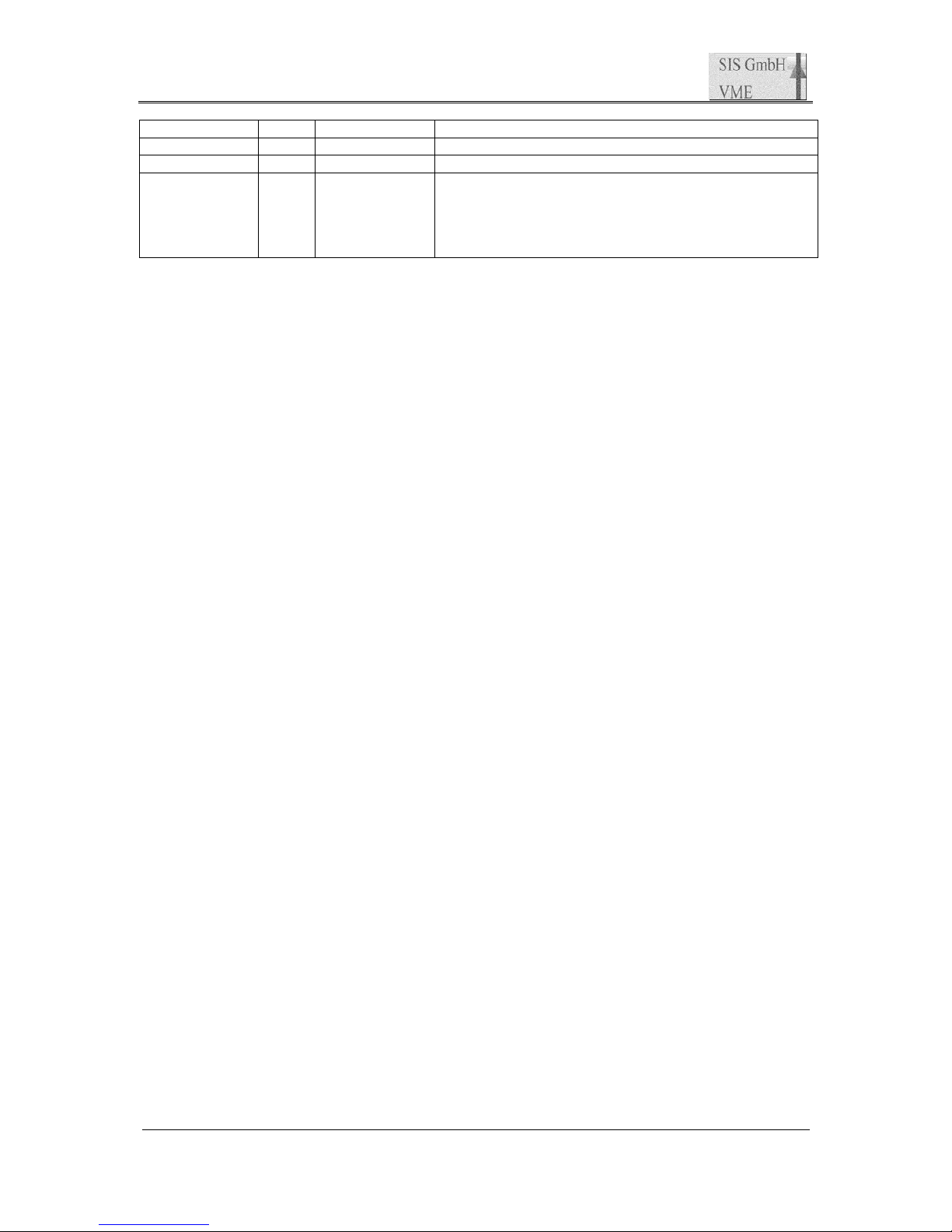
The base address is defined by the selected addressing mode, which is defined by jumper
array J1 and possibly SW4 and SW3 (in non geographical mode).
Function
EN_A32
reserved
EN_GEO SDRAM_SIZE open: 64 MByes
J1
SDRAM_SIZE closed: 512 MBytes
EN_A32 EN_GEO
Description
0 0 non A32 addressing, reserved for future use
0 1 non A32 addressing, reserved for future use
1 0 A32 addressing, address compared with SW3/SW4
1 1 A32 addressing, address compared with geographical address
0: jumper open, 1: jumper closed
The table below illustrates the possible base address settings.
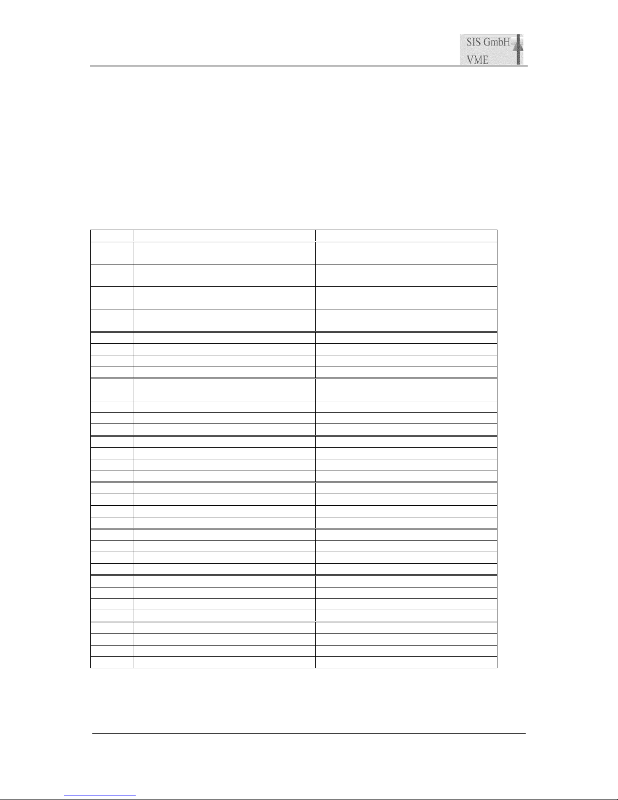
J1 Setting Bits
GEO 31 30 29 28 27 26 25 24
- SW4 SW3
x
y
y
y
GA4
GA3
GA2
GA1
GA0
Shorthand Explanation
SW3/SW4 Setting of rotary switch SW3 or SW4 respective
y don’t care
GA0-GA4 Geographical address bit as defined by the VME64x(P) backplane
Notes:
• This concept allows the use of the SIS3820 in standard VME as well as in VME64x
environments, i.e. the user does not have to use a VME64x backplane.
• The factory default setting is 0x38000000 (i.e. SW4=3, SW3=8, EN_A32 closed and
EN_GEO open/disabled)
Page 17

SIS Documentation SIS3820
VME Scaler
Page 17 of 79
6.1 Address map
Offset R/W Mode Function/Register
0x0 R/W D32 Control/Status register
0x4 R D32 Module Id. and firmware revision register
0x8 R/W D32 Interrupt configuration register
0xC R/W D32 Interrupt control/status register
0x10 R/W D32 Acquisition preset register
0x14 R D32 Acquisition count register
0x18 R/W D32 LNE prescale factor register
0x20 R/W D32 Preset value register counter group 1 (1 to 16)
0x24 R/W D32 Preset value register counter group 2 (17 to 32)
0x28 R/W D32 Preset enable and hit register
0x30 R/W D32 CBLT/Broadcast setup register
0x34 R/W D32 SDRAM page register
0x38 R D32 FIFO Word count register
0x3C R/W D32 FIFO Word count threshold register
0x40 R/W D32 HISCAL_START_PRESET
0x44 R D32 HISCAL_START_COUNTER
0x48 R D32 HISCAL_LAST_ACQ_COUNTER
0x100 R/W D32 (Acquisition) Operation mode register
0x104 R/W D32 Copy disable register
0x108 R/W D32 LNE channel select register (1 of 32)
0x10C R/W D32 PRESET channel select register ( 2 times 1 out of 16)
0x110 R/W D32 MUX_OUT channel select register (firmware 01 0B, 1 of 32,
note 2)
0x200 R/W D32 Inhibit/count disable register
0x204 W D32 Counter Clear register
0x208 R/W D32 Counter Overflow read and clear register
0x210 R D32 Channel 1/17 Bits 33-48
0x214 R/W D32 Veto external count inhibit register (firmware 01 09, note 2)
0x218 R/W D32 Test pulse mask register (firmware 01 0A, note 2)
0x300 R/W SDRAM Prom
0x310 R/W XILINX JTAG_TEST/JTAG_DATA_IN
0x314 W XILINX JTAG_CONTROL
future use R/W One wire Id. register
0x400 KA D32 (broadcast) Key reset
0x404 KA D32 (broadcast) Key SDRAM/FIFO reset
0x408 KA D32 (broadcast) Key test pulse
0x40C KA D32 (broadcast) Key Counter Clr
0x410 KA D32 (broadcast) Key VME LNE/clock shadow
0x414 KA D32 (broadcast) Key operation arm
0x418 KA D32 (broadcast) Key operation enable
0x41C KA D32 (broadcast) Key operation disable
0x420 KA D32
0x424 KA D32
0x428 KA D32
0x42C KA D32
Page 18
SIS Documentation SIS3820
VME Scaler
Page 18 of 79
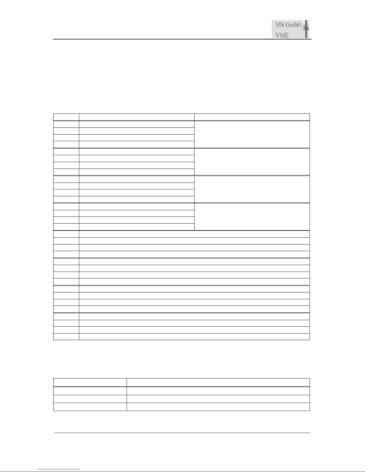
0x800 to 0x87C R D32/BLT32 Shadow registers
0xA00 to 0xA7C R D32/BLT32 Counter registers
0x800000 to
0xfffffc
W
R
D32/BLT32
D32/BLT32/
MBLT64/2eVme
SDRAM or FIFO space array
(address window for page of 8 Mbytes)
Notes:
1.) SDRAM (FIFO respective ) write access with active MCS mode will result in a VME
bus error. In MCS mode the memory is reserved for storage of the counter values.
2.) firmware 01 0A indicates revision 01 0A and higher unless otherwise
The shorthand KA stands for key address. Write access with arbitrary data to a key address
initiates the specified function
7 Register description
The function of the individual registers is described in detail in this section.
The first line after the subsection header (in Courier font) like:
#define SIS3820_CONTROL_STATUS 0x0 /* read/write; D32 */
refers to the sis3820.h header file.
Page 19
SIS Documentation SIS3820
VME Scaler
Page 19 of 79
7.1 Control/Status Register(0x, write/read)
#define SIS3820_CONTROL_STATUS 0x0 /* read/write; D32 */
The control register is in charge of the control of some basic properties of the SIS3820 board,
like enabling test pulse generators. It is implemented via a selective J/K register, a specific
function is enabled by writing a 1 into the set/enable bit, the function is disabled by writing a
1 into the clear/disable bit (which location is 16-bit higher in the register). An undefined
toggle status will result from setting both the enable and disable bits for a specific function at
the same time.
On read access the same register represents the status register.
Bit write Function read Function
31 Status external LATCH Bit2 (depending on
Input Mode)
30 Status external LATCH Bit1 (depending on
Input Mode)
29 Status external Input Bit2 (depending on
Input Mode)
28 Status external Input Bit1 (depending on
Input Mode)
27 Overflow
26 0
25 Status HISCAL operation enable
24 Status Operation armed
23 Status Operation SDRAM/FIFO Test
enabled
22 switch off reference pulser channel 1 (*) 0
21 counter test mode (*) 0
20 clear 25MHz test pulses (*) 0
19 0
18 Status Operation MCS enable (active)
17 0
16 switch off user LED (*) Status Operation Scaler enable (active)
15 0
14 0
13 0
12 0
11 0
10 0
9 0
8 0
7 0
6 switch on 50 MHz reference pulser channel 1 Status reference pulser
5 enable counter test mode Status counter test mode enable
4 enable 25MHz test pulses Status 25MHz test pulses
3 0
2 0
1 0
0 switch on user LED Status User LED (1=LED on, 0=LED off)
(*) denotes power up default setting, i.e. the power up reading of the register is 0x0
Page 20

SIS Documentation SIS3820
VME Scaler
Page 20 of 79
7.1.1 Counter test mode
VME Key test pulse signals will be counted by all (non inhibited) counters in test mode.
Counter test mode has to be activated for 25 MHz test pulse operation also.
7.1.2 25 MHz test pulse mode
All (non inhibited) scaler channels will count 25 MHz test pulses if this bit and the counter
test mode bit is set. From firmware 01 0A on you can use the test pulse mask register to
exclude selected channels from participating in test pulse counting.
7.1.3 Reference pulser channel 1
Channel 1 will count 50 MHz reference pulses (precision defined by the on board 100 ppm 50
MHz quarz) if this bit is set.
Note: test mode has priority over reference pulser, i.e. reference pulses will not be counted if
test mode (with or without 25 MHz test pulse mode) is active.
Page 21
SIS Documentation SIS3820
VME Scaler
Page 21 of 79
7.2 Module Id. and Firmware Revision Register (0x4, read)
#define SIS3820_MODID 0x4 /* read only; D32 */
This register reflects the module identification of the SIS3820 and its minor and major
firmware revision levels. The major revision level will be used to distinguish between
substantial design differences and experiment specific designs, while the minor revision level
will be used to mark user specific adaptations.
Bit Function Reading
31 Module Id. Bit 15
30 Module Id. Bit 14
29 Module Id. Bit 13
28 Module Id. Bit 12
3
27 Module Id. Bit 11
26 Module Id. Bit 10
25 Module Id. Bit 9
24 Module Id. Bit 8
8
23 Module Id. Bit 7
22 Module Id. Bit 6
21 Module Id. Bit 5
20 Module Id. Bit 4
2
19 Module Id. Bit 3
18 Module Id. Bit 2
17 Module Id. Bit 1
16 Module Id. Bit 0
0
15 Major Revision Bit 7
14 Major Revision Bit 6
13 Major Revision Bit 5
12 Major Revision Bit 4
11 Major Revision Bit 3
10 Major Revision Bit 2
9 Major Revision Bit 1
8 Major Revision Bit 0
7 Minor Revision Bit 7
6 Minor Revision Bit 6
5 Minor Revision Bit 5
4 Minor Revision Bit 4
3 Minor Revision Bit 3
2 Minor Revision Bit 2
1 Minor Revision Bit 1
0 Minor Revision Bit 0
7.2.1 Major revision numbers
Find below a table with major revision numbers used/reserved to date
Major revision number Application/user
0x01 Generic SIS3820 32 channel scaler design
0xE0 SIS3820-CLOCK
0xF0 SIS3820-LATCH
Page 22
SIS Documentation SIS3820
VME Scaler
Page 22 of 79
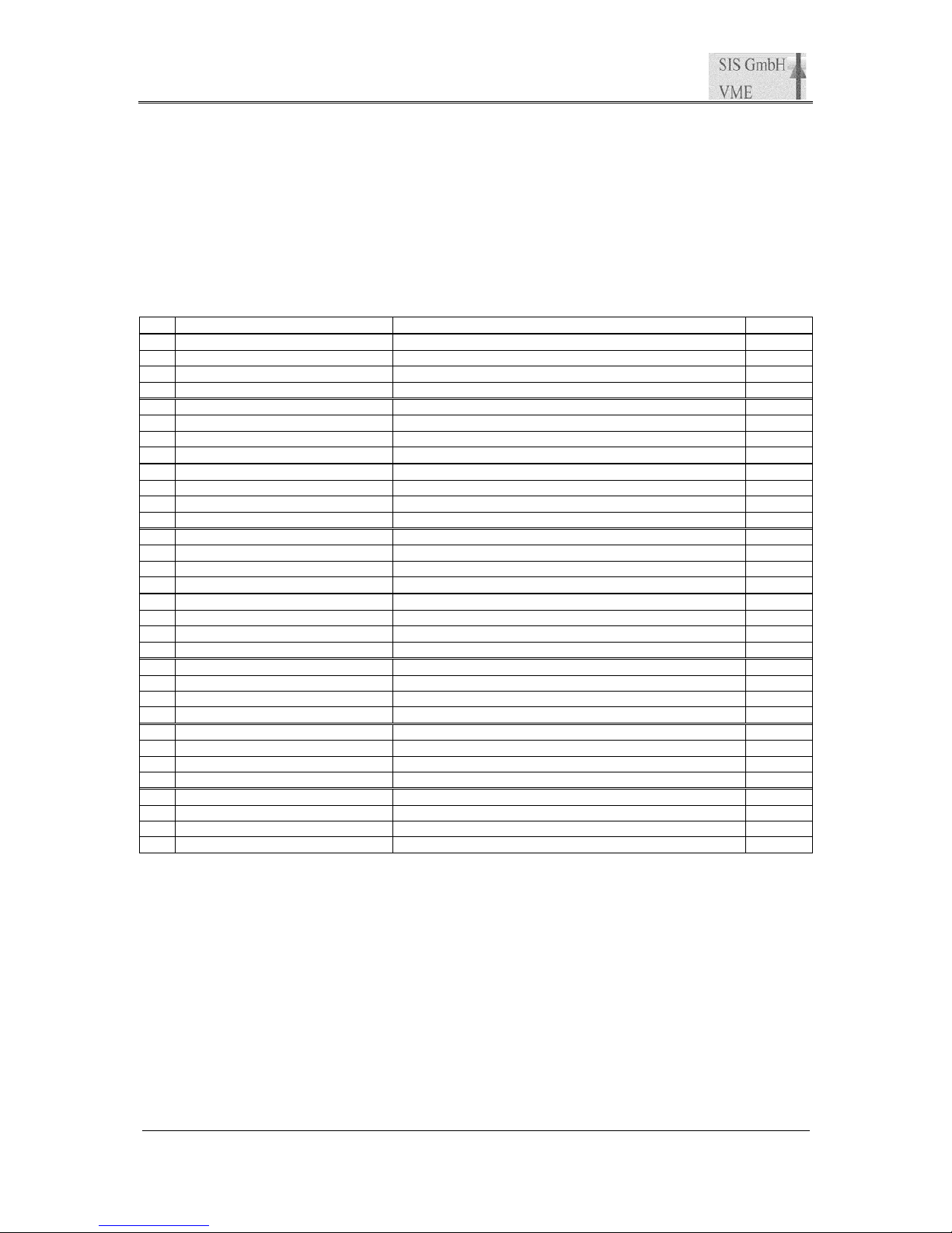
7.3 Interrupt configuration register (0x8)
#define SIS3820_IRQ_CONFIG 0x8 /* read/write; D32 */
In conjunction with the interrupt control register this read/write register controls the VME
interrupt behaviour of the SIS3820. Eight interrupt sources are foreseen, for the time being
four of them are associated with an interrupt condition, the others are reserved for future use.
The interrupter type is DO8 .
7.3.1 IRQ mode
In RORA (release on register access) mode the interrupt will be pending until the IRQ
source is cleared by specific access to the corresponding disable VME IRQ source bit. After
the interrupt is serviced the source has to be activated with the enable VME IRQ source bit
again.
In ROAK (release on acknowledge) mode , the interrupt condition will be cleared (and the
IRQ source disabled) as soon as the interrupt is acknowledged by the CPU. After the interrupt
is serviced the source has to be activated with the enable VME IRQ source bit again. ROAK
IRQ mode can be used in conjunction with the University of Bonn LINUX Tundra Universe
II driver by Dr. Jürgen Hannappel on Intel based VME SBCs.
Bit Function Default
31 0
... 0
16 0
15 0
14 0
13 0
12 RORA/ROAK Mode (0: RORA; 1: ROAK) 0
11 VME IRQ Enable (0=IRQ disabled, 1=IRQ enabled) 0
10 VME IRQ Level Bit 2 0
9 VME IRQ Level Bit 1 0
8 VME IRQ Level Bit 0 0
7 IRQ Vector Bit 7; placed on D7 during VME IRQ ACK cycle 0
6 IRQ Vector Bit 6; placed on D6 during VME IRQ ACK cycle 0
5 IRQ Vector Bit 5; placed on D5 during VME IRQ ACK cycle 0
4 IRQ Vector Bit 4; placed on D4 during VME IRQ ACK cycle 0
3 IRQ Vector Bit 3; placed on D3 during VME IRQ ACK cycle 0
2 IRQ Vector Bit 2; placed on D2 during VME IRQ ACK cycle 0
1 IRQ Vector Bit 1; placed on D1 during VME IRQ ACK cycle 0
0 IRQ Vector Bit 0; placed on D0 during VME IRQ ACK cycle 0
The power up default value reads 0x 00000000
Page 23
SIS Documentation SIS3820
VME Scaler
Page 23 of 79
7.4 Interrupt Control/Status register (0xC)
#define SIS3820_IRQ_CONTROL 0xC /* read/write; D32 */
The interrupt sources are enabled with the interrupt control register. The interrupt source is
cleared in the interrupt service routine. The status internal IRQ flag can be used for tests
without activating VME interrupt generation. It is set whenever an interrupt would be
generated if interrupting would be enabled in the interrupt configuration register.
fourth condition is reserved for future use.
Bit Function (w) (r) Default
31 1 Shot : IRQ_UPDATE Status IRQ source 7 (reserved) 0
30 unused Status IRQ source 6 (reserved) 0
29 unused Status IRQ source 5 (reserved) 0
28 unused Status IRQ source 4 (FIFO almost full) 0
27 unused Status IRQ source 3 (overflow) 0
26 unused Status IRQ source 2 (acquisition completed) 0
25 unused Status IRQ source 1 (FIFO threshold) 0
24 unused Status IRQ source 0 (LNE/clock shadow) 0
23 Clear IRQ source 7 Status flag source 7 0
22 Clear IRQ source 6 Status flag source 6 0
21 Clear IRQ source 5 Status flag source 5 0
20 Clear IRQ source 4 Status flag source 4 0
19 Clear IRQ source 3 Status flag source 3 0
18 Clear IRQ source 2 Status flag source 2 0
17 Clear IRQ source 1 Status flag source 1 0
16 Clear IRQ source 0 Status flag source 0 0
15 Disable IRQ source 7 Status VME IRQ 0
14 Disable IRQ source 6 Status internal IRQ 0
13 Disable IRQ source 5 0 0
12 Disable IRQ source 4 0 0
11 Disable IRQ source 3 0 0
10 Disable IRQ source 2 0 0
9 Disable IRQ source 1 0 0
8 Disable IRQ source 0 0 0
7 Enable IRQ source 7 Status enable source 7 (read as 1 if enabled, 0 if disabled) 0
6 Enable IRQ source 6 Status enable source 6 (read as 1 if enabled, 0 if disabled)
5 Enable IRQ source 5 Status enable source 5 (read as 1 if enabled, 0 if disabled) 0
4 Enable IRQ source 4 Status enable source 4 (read as 1 if enabled, 0 if disabled) 0
3 Enable IRQ source 3 Status enable source 3 (read as 1 if enabled, 0 if disabled) 0
2 Enable IRQ source 2 Status enable source 2 (read as 1 if enabled, 0 if disabled) 0
1 Enable IRQ source 1 Status enable source 1 (read as 1 if enabled, 0 if disabled) 0
0 Enable IRQ source 0 Status enable source 0 (read as 1 if enabled, 0 if disabled) 0
The power up default value reads 0x 00000000
Note: The clear IRQ source bits are relevant for edge sensitive IRQs only
Page 24
SIS Documentation SIS3820
VME Scaler
Page 24 of 79
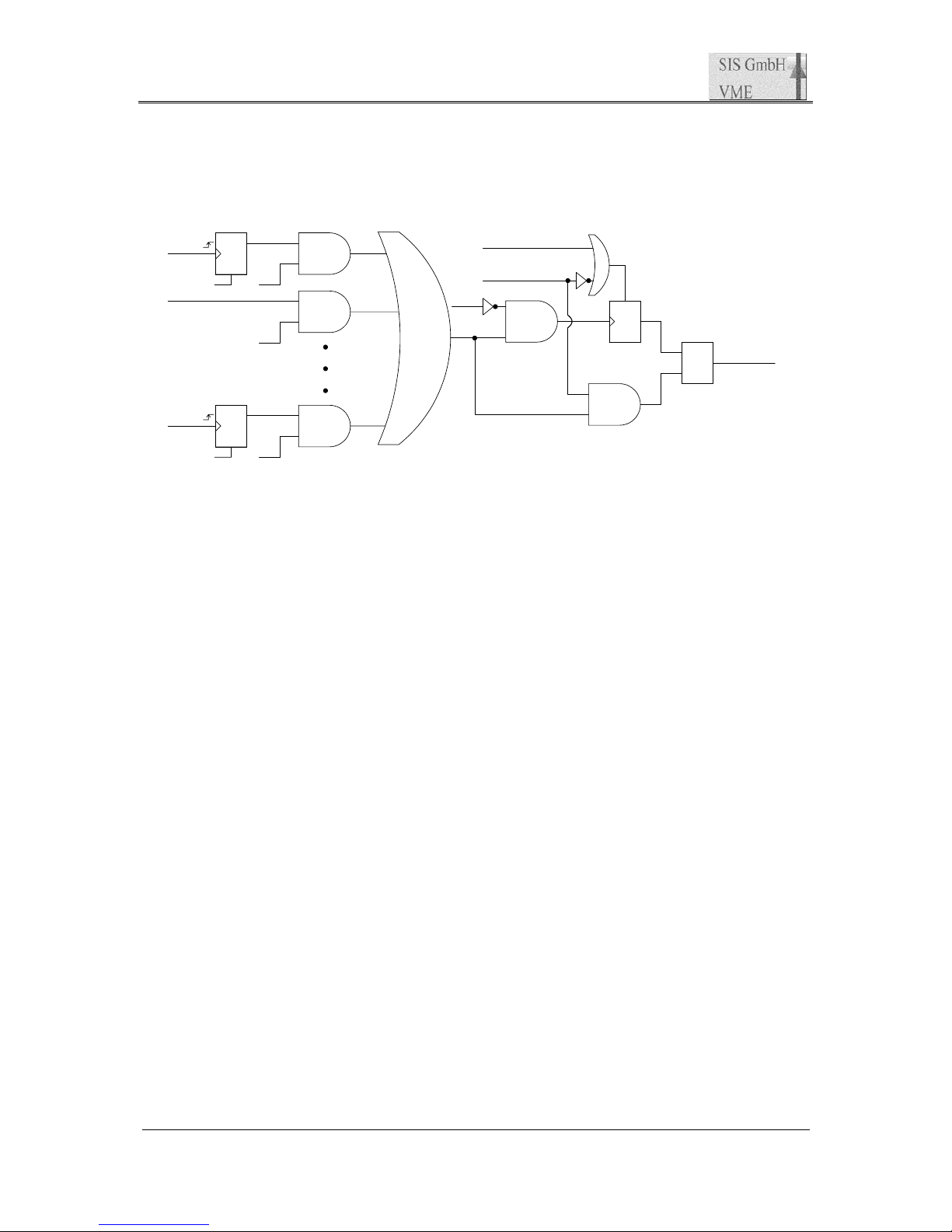
The generation of the status flags, the IRQ flags and the actual IRQ is illustrated with the
schematic below:
Note: Source 0 is shown as edge sensitive and source 1 as level sensitive input in the drawing
above. Which interrupt sources are edge and level sensitive may vary from firmware
implementation to firmware implementation.
7.4.1 Interrupt sources
A short explanation of the implemented interrupt sources is given in the following
subsections.
7.4.1.1 LNE/clock shadow (IRQ source 0; edge sensitive)
In multiscaler or multi channel scaler (MCS) mode interrupt source 0 is associated to the LNE
(load next event) signal. The interrupt is issued whenever a LNE signal triggers scaler value
transfer to memory. The interrupt will be induced by the rundown of the preset value if LNE
prescaling is active.
In scaler mode the LNE interrupt is driven by the clock shadow signal .
7.4.1.2 FIFO threshold (IRQ source 1; level sensitive)
The FIFO threshold IRQ source can be used for efficient readout in FIFO emulation mode.
The interrupt will be triggered as soon as the number of data words in memory will reach the
(non 0) value of the FIFO threshold register
AND
AND
AND
Enable 0
OR
Status IRQ
Source 0
Status IRQ
Source 1
Status IRQ
Source 7
Clear
Source 0
Enable 1
Enable 7
Source 1
Clear
Source 7
Status FLAG
Source 0
Status FLAG
Source 1
Status FLAG
Source 7
AND
Clear IRQ (ROAK case)
internal
VME_IRQ
AND
IRQ_Update
O
R
MUX
VME IRQ
IRQ ACK cycle
VME IRQ enable
IRQ (RORA case)
Page 25

SIS Documentation SIS3820
VME Scaler
Page 25 of 79
7.4.1.3 Acquisition completed/Preset reached (IRQ source 2; edge sensitive)
The number of counting periods to acquire data can be defined with the acquisition preset
register in MCS mode. The acquisition completed interrupt source can be used to trigger an
interrupt with this condition. The interrupt is issued as soon as the preset is reached in preset
scaler mode
7.4.1.4 Overflow (IRQ source 3; level sensitive)
The overflow interrupt source is triggered if one or more counters exceed the 32-bit range.
The overflow registers can be used to identify the channel that has caused the interrupt.
Overflow interrupt generation is active in non clearing mode only.
7.4.1.5 FIFO almost full (IRQ source 4; edge sensitive)
This interrupt source can be used to catch the FIFO almost full error condition. It is set if the
fill level of the SDRAM exceeds 64 MB-512 words in FIFO mode. The condition has to be
resolved by a KEY_SDRAM_FIFO_RESET.
Page 26
SIS Documentation SIS3820
VME Scaler
Page 26 of 79
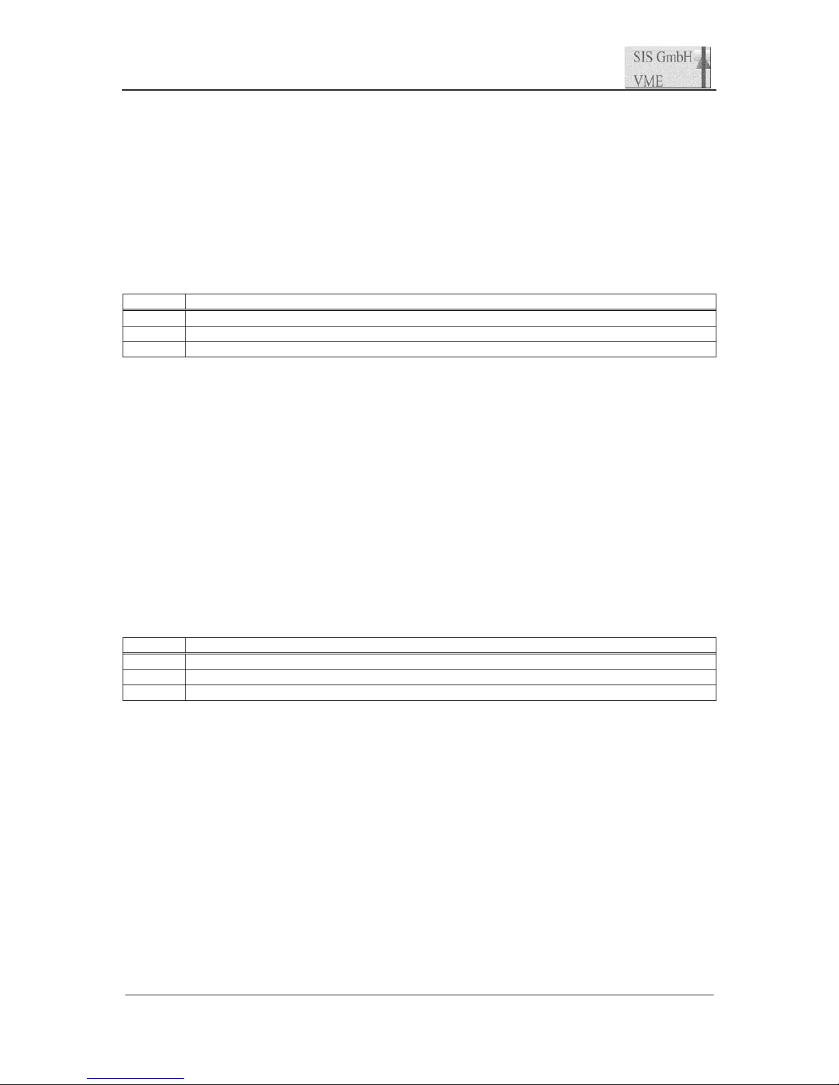
7.5 (0x10)Acquisition preset register
#define SIS3820_ACQUISITION_PRESET 0x10 /* read/write; D32 */
This read/write register allows you to define the number of counting periods to acquire in
MCS mode. The preset value is 32-bit wide. A preset value of 0 results in continuous MCS
operation.
Further LNEs are ignored after completion of acquisition until a key reset acquisition VME
access is performed. The completion flag is cleared upon reset acquisition also.
Bit Function
31 bit 31 of preset value
... ...
0 bit 0 of preset value
• The register can be used in scaler mode also
• it is not associated with a direct interrupt. Interrupt generation can be accomplished in
conjunction with the “acquisition completed (IRQ source 2, edge sensitive)
• The status flag of the active mode (scaler enabled e.g.) will be cleared upon completion
7.6 Acquisition count register (0x14)
#define SIS3820_ACQUISITION_COUNT 0x14 /* read D32 */
This 32-bit wide read only register holds the number of acquisitions. It is cleared with the
start operation and incremented with consecutive LNE pulses. The contents of the acquisition
count register is compared with the contents of the acquisition preset register if the later is non
zero. Acquisition is completed as soon as the acquisition count is greater or equal than the
acquisition preset value.
Bit Function
31 bit 31 of acquisition count
... ...
0 bit 0 of acquisition count
Page 27
SIS Documentation SIS3820
VME Scaler
Page 27 of 79
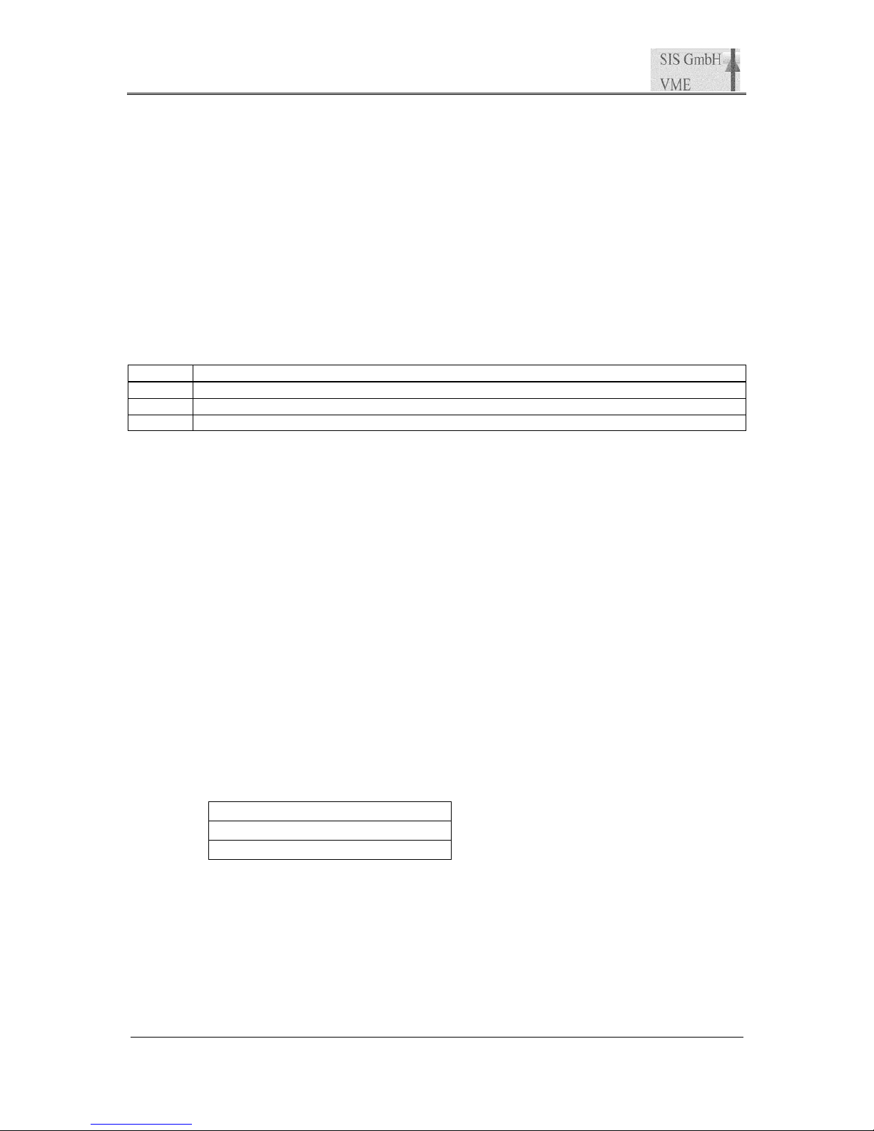
7.7 LNE Prescaler fact or register (0x18)
#define SIS3820_LNE_PRESCALE 0x18 /* read/write; D32 */
The LNE prescale factor register allows you to prescale the front panel LNE pulse (clock ticks
from an angular encoder e.g.), the internal 10 MHz pulse generator or the channel N (ChN)
LNE source. The prescale factor is a 32-bit value. The second case above allows you to run
the multiscaler with a fixed time slice length. The register can be reprogrammed while the
scaler acquires data as long as the user makes sure not to change the prescale factor while an
internal reload is in progress. The period between two CIP pulses is safe for reprogramming.
Programming the prescale factor to 0 results in routing the raw signal to the LNE. If the LNE
rate after the prescaler is higher than the possible maximum, excess LNE pulses are ignored,
the CIP output allows you to monitor the accepted LNE pulses.
Bit Function
31 LNE prescale factor bit 31
... ...
0 LNE prescale factor bit 0
If the new prescale factor is supposed to have an immediate effect (i.e. if the new prescale
factor and the input rate are smaller than the previous setting), following sequence has to be
used:
1.) disable LNE prescaler (write 0x0 to the LNE prescaler factor register)
2.) enable LNE prescaler (by writing the new LNE prescale value to the LNE prescaler factor
register)
The LNE prescale factor is given by register value+1.
If the an output mode with CIP front panel output is enabled, the CIP signal can be used to
synchronise external hardware to the actual LNE pulses after prescaling.
Example: If 9999 (decimal) is written to the LNE prescale factor register with the prescaler
and the 10 MHz to prescaler enabled (via bits 6 and 7 of the control register), the scaler will
get LNE pulses with a frequency of 1 KHz.
Following LNE sources are routed through the LNE prescaler if the prescale factor has a non
zero value:
external LNE (front panel signal)
internal 10 MHz
channel N (ChN)
Note 1: This implies, that software LNE pulses are not routed through the LNE prescaler,
they do always initiate a direct LNE/readout cycle
Note 2: The external LNE and channel N rate is limited to 5 MHz
Page 28
SIS Documentation SIS3820
VME Scaler
Page 28 of 79
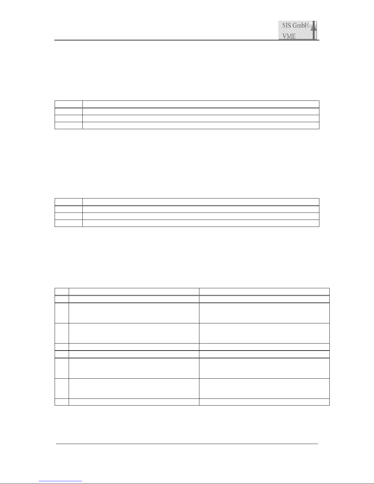
7.8 Preset value register counter group 1 (0x20)
#define SIS3820_PRESET_GROUP1 0x20 /* read/write; D32 */
The preset value for channels 1-16 is defined by this register. The preset channel select
register is used to define which of the 16 channels of the group is actually compared to the
preset value.
Bit Function
31 Preset bit 31
... ...
0 Preset bit 0
7.9 Preset value register counter group 2 (0x24)
#define SIS3820_PRESET_GROUP2 0x24 /* read/write; D32 */
The preset value for channels 17-32 is defined by this register. The preset channel select
register is used to define which of the 16 channels of the group is actually compared to the
preset value.
Bit Function
31 Preset bit 31
... ...
0 Preset bit 0
7.10 Preset Enable and Hit register (0x28)
#define SIS3820_PRESET_ENABLE_HIT 0x28 /* read/write; D32 */
This register is used to enable one or both counter groups for preset operation and provides
the information which group has reached the preset value.
Bit write Function read Function
18 none LNE latched preset reached status group 2
0: channel group 2 has not reached preset value
1: channel group 2 has reached preset value
17 none preset reached status group 2
0: channel group 2 has not reached preset value
1: channel group 2 has reached preset value
16 ENABLE group 2 Status ENABLE group 2
...
2 none LNE latched preset reached status group 1
0: channel group 1 has not reached preset value
1: channel group 1 has reached preset value
1 none preset reached status group 1
0: channel group 1 has not reached preset value
1: channel group 1 has reached preset value
0 ENABLE group 1 Status ENABLE group 1
At power up or after key reset the register the register will read 0.
Page 29

SIS Documentation SIS3820
VME Scaler
Page 29 of 79
7.11 CBLT/Broadcast setup register
#define SIS3820_CBLT_BROADCAST_SETUP 0x30 /* read/write; D32 */
This read/write register defines, whether the SIS3820 will participate in a CBLT and/or
Broadcast. The configuration of this register and the registers of other participating modules is
essential for proper CBLT and/or Broadcast behaviour.
CBLT is supported from the SDRAM in FIFO emulation mode (MCS Mode).
Bit Function
31 CBLT/Broadcast address bit 31
30 CBLT/Broadcast address bit 30
29 CBLT/Broadcast address bit 29
28 CBLT/Broadcast address bit 28
27 CBLT/Broadcast address bit 27
26 CBLT/Broadcast address bit 26
25 CBLT/Broadcast address bit 25
24 CBLT/Broadcast address bit 24
23 CBLT MAX Readout Length Bit 7
22 CBLT MAX Readout Length Bit 6
21 CBLT MAX Readout Length Bit 5
20 CBLT MAX Readout Length Bit 4
19 CBLT MAX Readout Length Bit 3
18 CBLT MAX Readout Length Bit 2
17 CBLT MAX Readout Length Bit 1
16 CBLT MAX Readout Length Bit 0
15 CBLT Geographical address bit 4 (use for Header and Trailer)
14 CBLT Geographical address bit 3
13 CBLT Geographical address bit 2
12 CBLT Geographical address bit 1
11 CBLT Geographical address bit 0
10 0
9 0
8 0
7 0
6 0
5 Enable Broadcast Master
4 Enable Broadcast
3 0
2 First (to be set to 1 on the first module in the CBLT chain)
1 Last (to be set to 1 on the last module in the CBLT chain)
0 enable CBLT (to be set to 1 on all modules in the CBLT chain)
The function/meaning of the CBLT and the geographical address is illustrated in section.
15.9.1.
Page 30
SIS Documentation SIS3820
VME Scaler
Page 30 of 79
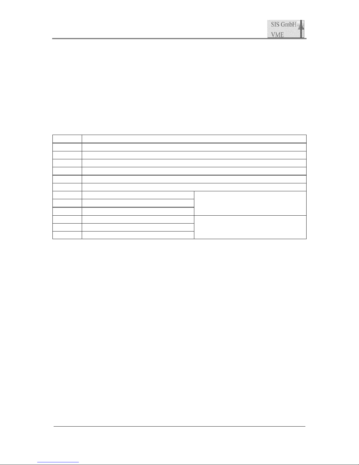
7.12 SDRAM page register (0x34)
#define SIS3820_SDRAM_PAGE 0x34 /* read/write; D32 */
This read/write register was implemented to reduce the address space that is occupied by the
SIS3820. The idea is to divide the SDRAM -that can have a size of up to 1024 Mbytes- into 8
MByte pages. The contents of the SDRAM page register defines what 8 MByte page is
addressed. The page will be incremented automatically during a block transfer (BLT32,
MBLT64, 2eVME)beyond a page boundary. This will allow you to read large chunks of
memory with the SIS3100 VME sequencer and similar hardware in one go.
The page number is not modified by the MCS scaler data acquisition process.
Bit Function
31 none, read as 0
... ...
9 none, read as 0
8 memory size bit: 0: 64 MB, 1: 512 MB
7 none, read as 0
6 none, read as 0
5 page number bit 5
4 page number bit 4
3 page number bit 3
used with 512 MByte strip
2 page number bit 2
1 page number bit 1
0 page number bit 0
used with 64 MByte strip
The power up value for the page number is 0.
Page 31
SIS Documentation SIS3820
VME Scaler
Page 31 of 79
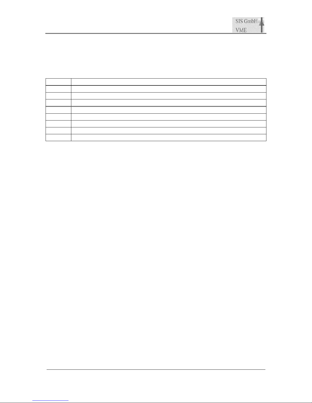
7.13 FIFO word counter/memory address pointer register (0x38)
#define SIS3820_FIFO_WORDCOUNTER 0x38 /* read; D32 */
This read only register holds SDRAM fill level information.
Bit Function
31 none, read as 0
... ...
28 none, read as 0
27 none, read as 0
26 word counter bit 26
... ...
1 word counter bit 1
0 word counter bit 0
The word counter is
• cleared upon SIS3820_KEY_RESET and SIS3820_KEY_SDRAM_FIFO_RESET
• incremented on data being written to SDRAM/FIFO (in MCS mode or SDRAM/FIFO
VME write test mode)
• decremented when data are read from the memory by VME
Note: if you read the same data from SDRAM more than once (in non FIFO mode), the word
counter will not reflect the actual fill level (i.e. FIFO mode is the main word counter
application).
SDRAM Address pointers (non VME accessible)
In FIFO Mode:
• the write pointer is reset upon SIS3820_KEY_RESET and
SIS3820_KEY_SDRAM_FIFO_RESET
• the write pointer is incremented upon SDRAM write cycles (MCS mode ..)
• the read pointer is decremented upon SDRAM VME read cycles
In SDRAM Mode:
• write and read pointers are reset upon SIS3820_KEY_RESET and
SIS3820_KEY_SDRAM_FIFO_RESET
• the write pointer is incremented upon SDRAM write cycles (MCS mode ..)
• the read pointer is defined by the VME address
An internal FIFO almost full flag, which blocks further writes/LNEs, is generated in FIFO
mode at 64 MBytes – 512 words (512 MBytes- 512 words respective). Data from up to two
LNE cycles may be pipelined and still be written to memory at this point. . This condition
reflects the error case and has to be avoided by readout in parallel to acquisition. It is
available as interrupt source 4 and has to be cleared with a
SIS3820_KEY_SDRAM_FIFO_RESET.
Page 32
SIS Documentation SIS3820
VME Scaler
Page 32 of 79
7.14 FIFO word counter threshold (0x3C)
#define SIS3820_FIFO_WORDCOUNT_THRESHOLD 0x3C /* read/write; D32 */
This read/write only register holds the fill level threshold for interrupt generation. The FIFO
word counter (longword, i.e. number of 32-bit words) threshold is compared to the FIFO
word counter register contents, an interrupt is generated as soon as the number of data words
in the SDRAM exceeds the threshold.
Bit Function
31 none, read as 0
... ...
28 none, read as 0
27 none, read as 0
26 FIFO word counter threshold bit 26
... ...
1 FIFO word counter threshold bit 1
0 FIFO word counter threshold bit 0
Notes:
• in principle memory strips of up to 512 MByte can be handled with this 27-bit deep FIFO
word counter threshold implementation
• the 3820 01 02 firmware will flag a FIFO error as soon as 64 MB – 512 longwords (512
MB –512 respective) are reached (with the possibility of data words still being buffered in
pipelines and being stored without data loss).
Page 33

SIS Documentation SIS3820
VME Scaler
Page 33 of 79
7.15 HISCAL_START_PRESET register (0x40)
#define SIS3820_HISCAL_START_PRESET 0x40 /* read/write; D32 */
The number of scans in HISCAL operation can be preset/limited with this 32-bit deep
register. The An entry of 0 (power up default) results in scanning operation until a KEY reset
or KEY HISCAL_OPERATION_DISABLE command is issued.
7.16 HISCAL_START_COUNTER register (0x44)
#define SIS3820_HISCAL_START_COUNTER 0x44 /* read only; D32 */
This 32-bit deep register holds the number of scans/starts in HISCAL operation. The register
content is updated with the start signal/pulse.
7.17 HISCAL_LAST_ACQ_COUNTER register (0x48)
#define SIS3820_LAST_ACQ_COUNTER 0x48 /* read only; D32 */
This 32-bit deep register holds the number of bins of the last scan (i.e. the contents of the
acquisition count register at the end of the scan). It is updated with the start in HISCAL
operation.
Page 34
SIS Documentation SIS3820
VME Scaler
Page 34 of 79
7.18 (Acquisition) Operation Mode register (0x100)
#define SIS3820_ACQUISITION_MODE 0x100 /* read/write; D32 */
Bit Function Default
31 reserved 0
30 Operation Mode bit 2 0
29 Operation Mode bit 1 0
28 Operation Mode bit 0 0
27 Reserved 0
26 Reserved 0
25 Reserved 0
24 reserved 0
23
Control outputs inverted
0
22 reserved 0
21
Control output mode bit 1
0
20
Control output mode bit 0
0
19
Control inputs inverted
0
18
Control input mode bit 2
0
17
Control input mode bit 1
0
16
Control input mode bit 0
0
15 reserved 0
14 HISCAL_START_SOURCE_BIT 0
13
select SDRAM add mode
0
12
select SDRAM mode
0
11 Reserved 0
10 Reserved 0
9
Arm/Enable source bit 1
0
8
Arm/Enable source bit 0
0
7 Reserved 0
6
LNE source bit 2
0
5
LNE source bit 1
0
4
LNE source bit 0
0
3
data format bit 1
0
2
data format bit 0
0
1 Reserved 0
0
select non clearing mode
0
The power up default value reads 0x 00000000
7.18.1 Modes of Operation modes (Bits 30:28)
Op Mode bit 2 Op Mode bit 1 Op Mode bit 0
Mode of operation
0 0 0 Scaler/Counter, Latching Scaler, Preset Scaler
0 0 1 reserved
0 1 0 Multi channel Scaler
0 1 1 reserved
1 0 0 reserved
1 0 1 reserved
1 1 0 reserved
1 1 1 SDRAM/FIFO VME write test mode
Page 35

SIS Documentation SIS3820
VME Scaler
Page 35 of 79
7.18.2 Input modes (Bits 18:16)
The SIS3820-SCALER board has 4 control inputs. They can be assigned to different signals
with the 3 input modes bit of the acquisision/operation mode register as listed in the table
below. All inputs can be inverted with the control inputs inverted bit of the same register.
Control Input Mode
Input assignment
Mode 0 input 1 -> no function
(bit2=0, bit1=0, bit0=0) input 2 -> no function
input 3 -> no function
input 4 -> no function
Mode 1 input 1 -> external next pulse (LNE)/clock shadow
(bit2=0, bit1=0, bit0=1) input 2 -> external user bit 1
input 3 -> external user bit 2
input 4 -> inhibit LNE
Mode 2 input 1 -> external next pulse (LNE) /clock shadow
(bit2=0, bit1=1, bit0=0) input 2 -> external user bit 1
input 3 -> inhibit counting
input 4 -> inhibit LNE
Mode 3 input 1 -> external next pulse (LNE) /clock shadow
(bit2=0, bit1=1, bit0=1) input 2 -> external user bit 1
input 3 -> external user bit 2
input 4 -> inhibit counting
Mode 4 input 1 -> inhibit counting channels 1-8
(bit2=1, bit1=0, bit0=0) input 2 -> inhibit counting channels 9-16
input 3 -> inhibit counting channels 17-24
input 4 -> inhibit counting channels 25-32
Mode 5 input 1 -> external next pulse (LNE)
(bit2=1, bit1=0, bit0=1) input 2 -> external HISCAL_START (time reset/start pulse)
input 3 -> no function
input 4 -> no function
Mode 6 input 1 -> external next pulse (LNE) /clock shadow
(bit2=1, bit1=1, bit0=0) input 2 -> inhibit counting
input 3 -> clear all counters
input 4 -> external user bit 1
Modes 7 (reserved) input 1 -> no function
input 2 -> no function
input 3 -> no function
input 4 -> no function
Note: following LNE sources are affected by the LNE inhibit input
external LNE (front panel signal)
internal 10 MHz
channel N (ChN)
Page 36
SIS Documentation SIS3820
VME Scaler
Page 36 of 79
7.18.3 Output mode (Bits 21:20)
The SIS3820-SCALER board has 4 control outputs. They can be assigned to different signals
with the 2 output modes bit of the acquisision/operation mode register as listed in the table
below. All outputs (except the selected MUX OUT channel in mode 3) can be inverted with
the control outputs inverted bit of the same register.
Control Output Mode
Output assignment
Mode 0 output 5 -> Scaler mode : LNE pulse ; MCS Mode: CIP
(bit1=0, bit0=0) output 6 -> SDRAM empty
output 7 -> SDRAM threshold
output 8 -> User output (Led)
Mode 1 output 5 -> Scaler mode : LNE pulse ; MCS Mode: CIP
(bit1=0, bit0=1) output 6 -> Enabled
output 7 -> 50 MHz
output 8 -> User output (User LED)
Mode 2 output 5 -> Scaler mode : LNE pulse ; MCS Mode: CIP
(bit1=1, bit0=0) output 6 -> 10 MHz (20ns pulse)
output 7 -> 10 MHz (20ns pulse)
output 8 -> User output (User LED)
Modes 3 (01 0A onward) output 5 -> Scaler mode : LNE pulse ; MCS Mode: CIP
(bit1=1, bit0=1) output 6 -> 10 MHz (20ns pulse)
output 7 -> selected MUX OUT channel
output 8 -> User output (User LED)
Note: The user output is switched on and off with the same bit of the control register as the
user LED.
7.18.4 HISCAL_START_SOURCE_BIT (Bit 14)
The HISCAL_START_SOURCE_BIT defines whether the HISCAL_START is derived from
a VME KEY Start or from the HISCAL_START front panel input (input 2 with input
mode=5)
HISCAL_START_SOURCE_BIT HISCAL_START_SOURCE
0 VME_KEY_START
1 external HISCAL_START
(in conjunction with input mode 5)
Page 37
SIS Documentation SIS3820
VME Scaler
Page 37 of 79
7.18.5 SDRAM mode (Bit 12) and SDRAM add mode (Bit 13)
The SDRAM mode bit defines whether the the SIS3820 is operated in SDRAM or FIFO
emulation mode
In SDRAM add mode the SIS3820 operates in SDRAM mode always (independent of the
SDRAM mode bit setting). An SDRAM add bit setting of one in combination with MCS
mode of operation results in HISCAL (hsitogramming scaler) operation.
SDRAM add mode bit SDRAM mode bit Mode
0 0 FIFO emulation
0 1 SDRAM
1 0 SDRAM
1 1 SDRAM
7.18.6 Arm/enable source
The two arm/enable source bits define what signal the enable is derived from. In channel N
source mode the LNE channel register defines what scaler channel the enable signal is derived
from.
Arm/Enable Bit 1 Arm/Enable Bit 0 Arm/Enable source
0 0 LNE Front panel control signal
0 1 Channel N (ChN)
1 0 reserved
1 1 reserved
Notes:
1.) be aware, that the front panel control signal is active with input modes 1, 2, 3, 5 and 6
only
2.) ChN stands for the selected LNE channel
Page 38
SIS Documentation SIS3820
VME Scaler
Page 38 of 79
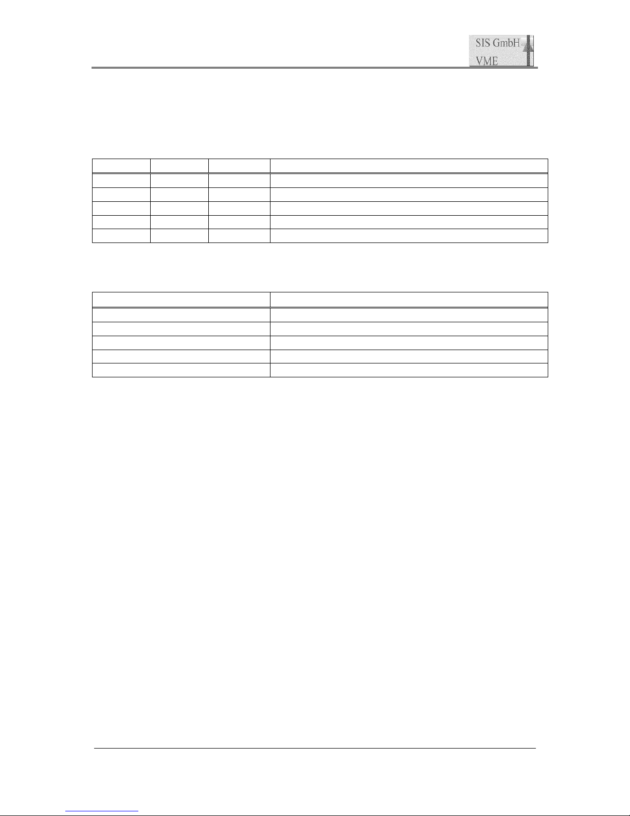
7.18.7 LNE source
The three LNE source bits define what signal the LNE (load next event) signal is derived
from. In channel N source mode the LNE channel register defines what scaler channel the
LNE signal is derived from.
LNE Bit 2 LNE Bit 1 LNE Bit 0 LNE source
0 0 0 VME key address only (ignore front panel signals)
0 0 1 Front panel control signal
0 1 0 10 MHz internal pulser
0 1 1 Channel N (ChN)
1 0 0 Preset Scaler N (MCS only)
LNE sources can be prescaled with the LNE prescaler where needed. The LNE prescaler is
active if the prescale factor register is loaded with a non zero value.
Routed through LNE prescaler if ≠ 0
LNE source
no VME key address only (ignore front panel signals)
yes Front panel control signal
yes 10 MHz internal pulser
yes Channel N (ChN)
no Preset Scaler N
Note 1: The maximum input frequency for the channel N or front panel LNE is limited to 10
MHz
Note 2: The external LNE and channel N rate is limited to 5 MHz
Page 39
SIS Documentation SIS3820
VME Scaler
Page 39 of 79
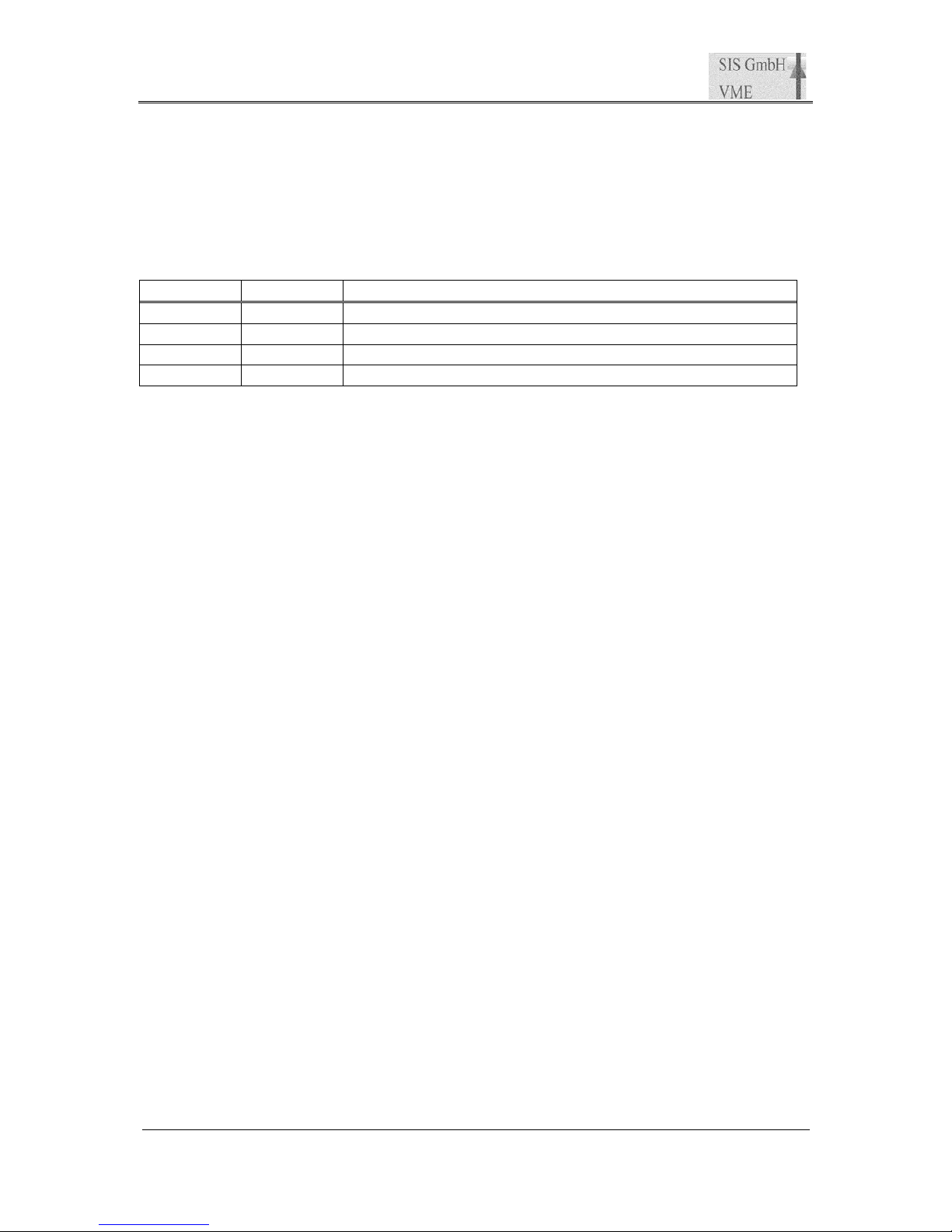
7.18.8 Data format
The data format bits allow you to select between a straight 32-bit and a 24-bit mode with
information from the two user inputs and channel information. For low rate and/or short dwell
time environments data reduction and lower dwell times can be accomplished by reduction of
the scaler depth to 16-bit or even 8-bit. Two respective four scaler values are packed into one
32-bit word in that case.
Format Bit 1 Format Bit 0 Data Format
0 0 32-bit
0 1 24-bit with user bit and channel information
1 0 16-bit (MCS only)
1 1 8-bit (MCS only)
A more detailed description of the data formats is given in section 8.
7.18.9 Clearing/non clearing
This bit decides, whether the scaler values are cleared upon LNE/clock shadow, or whether
the counter contents will be preserved and the accumulated counts will be stored to
SDRAM/to the shadow registers. The power up mode defaults to clearing, i.e. the number of
counts since the last readout cycle will be stored to SDRAM/to the shadow registers.
Refer to section 15.6 for a description of the function/behavior internal counter logic
Note: The overflow logic (generation of overflow IRQ e.g.) is active in non clearing mode
only.
Page 40
SIS Documentation SIS3820
VME Scaler
Page 40 of 79
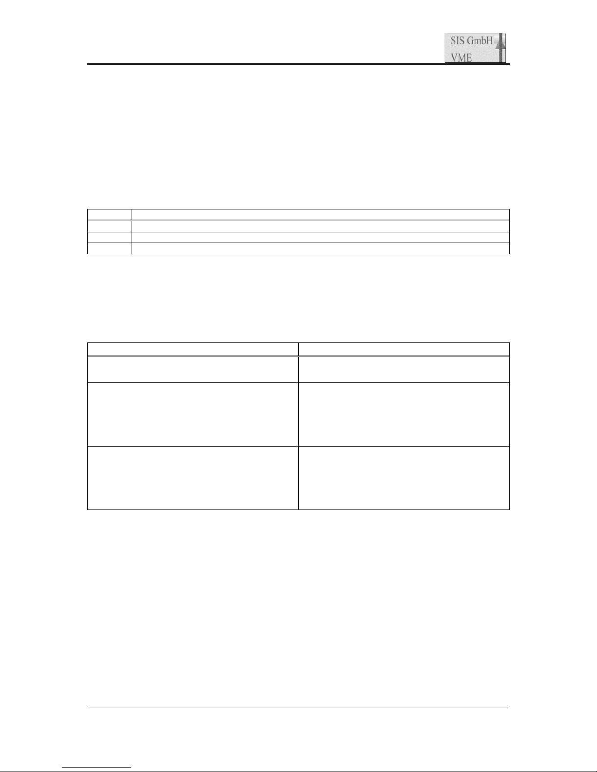
7.19 Copy disable register (0x104)
#define SIS3820_COPY_DISABLE 0x104 /* read/write; D32 */
This read/write register allows for exclusion of channels from the LNE (MCS mode )
The full copy loop is executed in pattern mode. Channels with their corresponding bit set in
the copy disable register are excluded from the copy process.
The minimum dwell time depend on the number of active channels and the selected data
format (refer to section 15.2 for a table of measured minimum dwell times).
Bit Function
31 copy disable bit channel 32
... ...
0 copy disable bit channel 1
Examples: If 0xFFFF is written to the copy disable register, channels 17 through 32 data
will be copied to memory, if 0xFFFF0000 is set channels 1 through 16 will be stored.
Note on copy disable behavior/limitations:
Data forma Copy disable behavior/limitations
32 or 24-bit Arbitrary channels can be disabled in a
selective fashion
16-bit Groups of 2 channel pairs are copied
Ch1 and 2, Ch2 and 4 e.g.
The corresponding dual channel group is
copied if the disable bit of the first channel of
the group (Ch1, 3, e.g.) is not set
8-bit Groups of 4 channel are copied
Ch1, 2, 3 and 4, Ch5, 6, 7 and 8 e.g.
The corresponding four channel group is
copied if the disable bit of the first channel of
the group (Ch1, 5, e.g.) is not set
Page 41
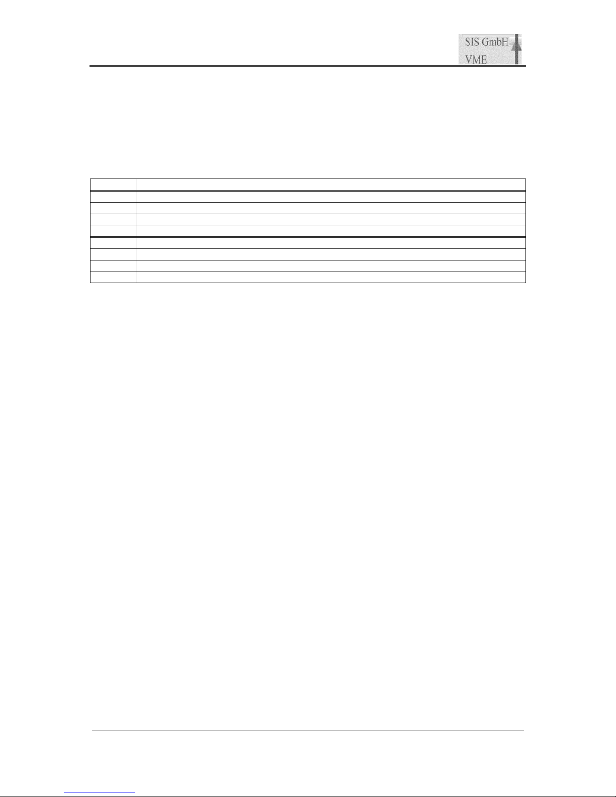
SIS Documentation SIS3820
VME Scaler
Page 41 of 79
7.20 LNE channel select register (0x108)
#define SIS3820_LNE_CHANNEL_SELECT 0x108 /* read/write; D32 */
This read/write register allows to define which of the 32 front panel scaler channels is used as
LNE source in LNE channel N mode. The LNE channel has to be selected before the counting
process is started and can not be changed during acquisition.
Bit Function
31 no function, read as 0
... ...
5 no function, read as 0
4 bit 4 of LNE channel
3
2
1 ...
0 bit 0 of LNE channel
Notes:
1.) The maximum input frequency for the LNE channel is limited to 10 MHz
2.) An inhibit of the selected channel (front panel or selective count disable) is ignored
Hint: make sure to activate the channel N LNE source in the acquisition/operation mode
register
Page 42
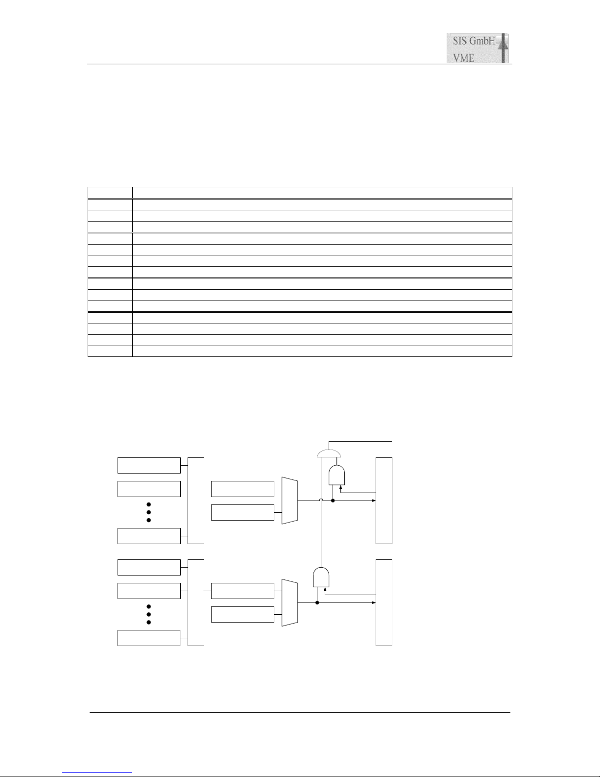
SIS Documentation SIS3820
VME Scaler
Page 42 of 79
7.21 PRESET channel select register (0x10C)
#define SIS3820_PRESET_CHANNEL_SELECT 0x10C /* read/write; D32 */
This read/write register allows to define which of the 32 front panel scaler channels is used as
LNE source in LNE channel N mode. The LNE channel has to be selected before the counting
process is started and can not be changed during acquisition. The channels are divided into
two groups of 16 channels each due to the architecture of the SIS3820.
Bit Function
31 no function, read as 0
... ...
20 no function, read as 0
19 bit 3 of PRESET channel select group2
18 ...
17 ...
16 bit 0 of PRESET channel select group2
15 no function, read as 0
... ...
4 no function, read as 0
3 bit 3 of PRESET channel select group1
2 ...
1 ...
0 bit 0 of PRESET channel select group1
Example: a setting of 0x00000004 selects channel 5 as preset/ChN LNE source
7.21.1 Preset scheme
The overall preset scheme of the SIS3820 scaler is illustrated below.
Scaler channel 32
Scaler channel 31
Scaler channel 17
Preset channel sel ect (17-32)
selected scaler channel
preset value group 2
Scaler channel 16
Scaler channel 15
Scaler channel 1
Preset channel s elect (1-16)
selected scaler channel
preset value group 1
comparecompare
OR
stop conditio n
Preset enable and hit (bits 16,17)Preset enable and hit ( bits 0,1)
AND
AND
Page 43
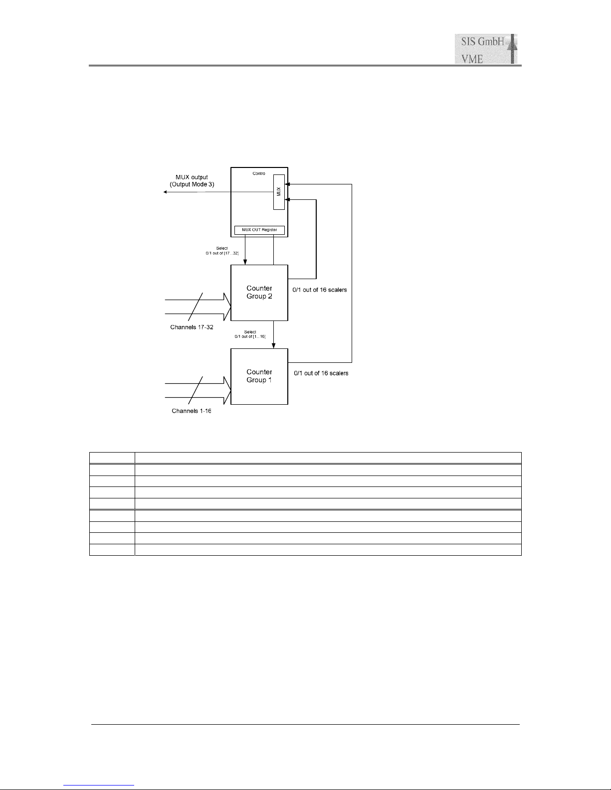
SIS Documentation SIS3820
VME Scaler
Page 43 of 79
7.22 MUX OUT channel select register (0x110)
#define SIS3820_MUX_OUT_CHANNEL_SELECT 0x110 /* read/write; D32 */
MUX functionality (available from firmware 01 0A on) allows to route one of the 32 scaler
input signals to an external instrument like a visual rate meter e.g.
Register Bit assignments:
Bit Function
31 no function, read as 0
... ...
5 no function, read as 0
4 bit 4 of OUT_MUX channel
3
2
1 ...
0 bit 0 of OUT_MUX channel
Notes:
1.) The power up default is0x0 (i.e. scaler channel 0 is routed to the output as soon as output
mode 3 is activated)
2.) MUX_OUT mode requires output mode 3
Example:
Channel 5 (channels counted from 0 to 31) is passed to output 7 with bit 0 and 2 of the MUX
OUT channel select register set and output mode 3 enabled
Page 44
SIS Documentation SIS3820
VME Scaler
Page 44 of 79
7.23 Inhibit/count disable register (0x200)
#define SIS3820_INHIBIT 0x200 /* read/write; D32 */
This read/write register is used for software inhibit of individual channels or arbitrary channel
groups. The inhibit condition is an OR of the front panel inhibit (where activated) and the
inhibit register.
Bit Function
31 0: enable /1: inhibit channel 32 counting
... ...
0 0: enable /1: inhibit channel 1 counting
At power up or after key reset the register the register will read 0, i.e. all scaler channels are
active.
7.24 Counter clear register (0x204)
#define SIS3820_COUNTER_CLEAR 0x204 /* write only; D32 */
On write access to this register each channel can be cleared individually by the setting of the
corresponding bit.
Bit write Function
31 1: clear channel 32
... ...
0 1: clear channel 1
7.25 Counter Overflow register (0x208)
#define SIS3820_COUNTER_OVERFLOW 0x208 /* read/write; D32 */
This register holds the information on which channel has run into overflow condition.
On write access to this register the overflow bits of each channel can be cleared individually
by the setting of the corresponding bit.
Bit write Function read Function
31 1: clear overflow bit of channel 32 Status of Overflow bit of channel 32
... ... ...
0 1: clear overflow bit of channel 1 Status of Overflow bit of channel 1
Page 45
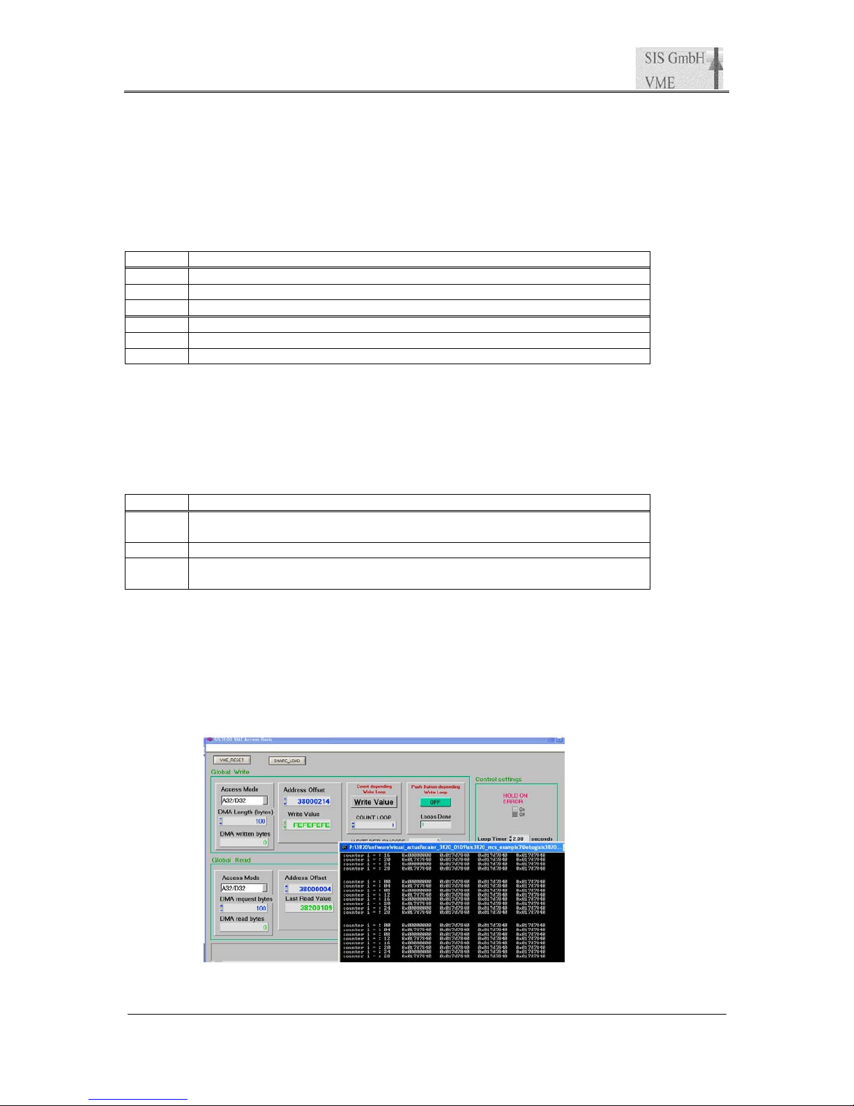
SIS Documentation SIS3820
VME Scaler
Page 45 of 79
7.26 Channel 1/17 Bits 33-48 register (0x210)
#define SIS3820_COUNTER_48BIT_EXTENSION 0x210 /* read only D32 */
This register holds the upper 16 bits of channels 1 and 17 (from firmware version 01 04
onwards). It is used in scaler mode (and typically it will make sense in non clearing mode
mainly)
Bit read Function
31 Bit 48 of scaler channel 17
... ...
16 Bit 33 of scaler channel 17
15 Bit 48 of scaler channel 1
...
0 Bit 33 of scaler channel 1
7.27 Veto external count inhibit register (0x214)
#define SIS3820_VETO_EXTERNAL_COUNT_INHIBIT 0x214 /* r/w D32 */
This register can be used to veto the external inhibit (input modes 1, 2, 3, 4 and 6) for
individual scaler channels. By default the veto function is switched off for all channels.
Bit Function
31 Veto external count inhibit channel 32
0: do not veto (power up default), 1: veto external inhibit
...
0 Veto external count inhibit channel 1
0: do not veto (power up default), 1: veto external inhibit
Application example: measure up to 4 (input mode 4) gate open/closed ratios with internal
(channel 1) or external (other channels) reference clocks. By writing 0xFEFEFEFE to the
register and using input mode 4 you can use channel 1, 9, 17 and 25 gated with control input
1, 2, 3 and 4 respective as reference clocks (as shown in the screen dump below with all
channels counting with the 25 MHz internal test pulser and all control inputs set).
Page 46
SIS Documentation SIS3820
VME Scaler
Page 46 of 79
7.28 Test pulse mask register (0x218)
#define SIS3820_TEST_PULSE_MASK 0x218 /* r/w D32 */
This register can be used to mask the 25 MHz test pulser from selected channels.
Bit Function
31 Mask test pulser channel 32
0: do not mask (power up default), 1: mask test pulser
...
0 Mask test pulser channel 1
0: do not mask (power up default), 1: mask test pulser
Application: This register is particularly useful in combination with the veto external count
inhibit register. and with input mode 4 (4 count inhibit groups) . You can use the 25 MHz test
pulser on channels 9, 17 and 25 and the 50 MHz reference pulser on channel 1 e.g. in
combination with the proper veto external count inhibit pattern set to measure the inhibit set
/no inhibit set fraction of the 4 control inputs.
7.29 SDRAM SPD register (0x300)
#define SIS3820_SDRAM_EEPROM_CTRL_STAT 0x300 /* read/write; D32 */
This register allows access to the serial PROM on the SDRAM memory strip of the SIS3820.
Refer to the Visual C++ example sis3820_sdram_eeprom.c for an example on the use of the
register.
Bit write Function read Function
31 none 0
... ... ...
12 none 0
11 none 0
10 none 0
9 none SDA_IN
8 none SDA_IN_LATCH
7 none 0
... ...
4 none 0
3 0
2 SDA_OUT_EN (1: enable SDA) 0
1 SDA_OUT (serial data out) 0
0 SCL (serial clock) 0
Page 47
SIS Documentation SIS3820
VME Scaler
Page 47 of 79
7.30 JTAG_TEST register
#define SIS3820_JTAG_TEST 0x310 /* write; D32; */
This register is used in the firmware upgrade process over VME only. A TCK is generated
upon a write cycle to the register.
Bit write Function
31 none
... ...
4 none
3 none
2 none
1 TMS
0 TDI
7.31 JTAG_DATA_IN register
#define SIS3820_JTAG_DATA_IN 0x310 /* read; D32; */
This register is used in the firmware upgrade process over VME only. It is at the same address
as the JTAG_TEST register and is used in read access. It operates as a shift register for TDO.
The contents of the register is shifted to the right by one bit with every positive edge of TCK
and the status of TDO is transferred to Bit 30. Bit 31 reflects the current value of TDO during
a read access.
7.32 JTAG_CONTROL register
#define SIS3820_JTAG_CONTROL 0x314 /* write only; D32;
*/
This register is used in the firmware upgrade process over VME only.
Bit write Function
31 none
... ...
4 none
3 none
2 none
1 none
0 1: Enable JTAG output
Page 48
SIS Documentation SIS3820
VME Scaler
Page 48 of 79
7.33 One wire Id. register (tbd)
(not implemented in 3820 01 01/02 firmware)
#define SIS3820_ONE_WIRE 0xtbd /* read/write; D32; */
A DS2430 256-Bit 1-wire EEPROM is installed on the SIS3820 to store the serial number of
the module. This information is stored in the 64-bit
A DS2430 256-Bit 1-wire EEPROM is installed on the SIS3820 to store the serial number of
the module. This information is stored in the 64-bit application register of the DS2430 in the
factory.
Offset Contents Example SIS3820-64 SN 10
0 0x38
1
Module Id.
0x20
2 0x00
3
SDRAM
size
0x64
4 0x00
5 0x00
6 0x00
7
Serial
Number
0x0A
Note: Module Id. and SDRAM size are stored in hexadecimal form for better readability, the
serial number is stored as straight 32-bit decimal value.
Refer to the PDF data sheet of the DS2430 and the LINUX example program rom_read.c on
the SIS3820 documentation CDROM for details on the operation of the EEPROM.
Bit Read function Write function
31 0 not used
... ...
16 0 not used
15 BUSY cmd RESET
14 Present cmd WRITE
13 0 cmd READ
12 0 reserved
11 0 reserved
10 0 reserved
9 reserved reserved
8 reserved reserved
7 read datum bit7 write datum bit7
6 read datum bit6 write datum bit6
5 read datum bit5 write datum bit5
4 read datum bit4 write datum bit4
3 read datum bit3 write datum bit3
2 read datum bit2 write datum bit2
1 read datum bit1 write datum bit1
0 read datum bit0 write datum bit0
Page 49

SIS Documentation SIS3820
VME Scaler
Page 49 of 79
7.34 FIFO address space (0x800000-0xFFFFFC)
#define SIS3820_FIFO_BASE 0x800000 /* read only; D32/BLTs */
Scaler data can be read from the FIFO address space in FIFO emulation mode. Both single
cycle (D32) and block transfer modes (BLT32, MBLT64, 2eVME) are supported. The FIFO
address space spans 8 MBytes (or 2 M long words) to allow for block transfer with auto
address incrementing VME masters.
A VME bus error (BERR) is driven actively by the SIS3820 if you attempt to read from an
empty FIFO.
7.34.1 non incrementing VME master
With a non auto incrementing VME master (like the SIS3100 in FIFO mode e.g.) you can
read an arbitrary amount of data (typically defined by the current value of the FIFO word
counter register)in one block transfer from the first address of the FIFO address space.
Blocking into smaller blockletts is handled by the hardware without user intervention. This
results in optimum VME throughput as minimum setup time is involved.
7.34.2 incrementing VME master
Most VME masters use address auto incrementing on block transfers. The FIFO address space
of 8 MBytes is a good compromise for large memories also. The user has to set up several
block transfers to read larger portions of memory.
7.35 SDRAM address space (0x800000-0xFFFFFC)
#define SIS3820_SDRAM_BASE 0x800000 /* read only; D32/BLTs */
For larger memories than 64 MBytes, SDRAM sections (pages) of 64 MBytes are selected
with the SDRAM page register.
Page 50
SIS Documentation SIS3820
VME Scaler
Page 50 of 79
8 Data Format
The SIS3820 has 4 different data formats. They are defined by the data format bits of the
acquisition/operation mode registermode . Non MCS data format is the same as 32-bit MCS.
8 and 16-bit mode were implemented to achieve both lower minimum dwell times and data
volume reduction in low count rate/short dwell time environments.
MCS Bit 1 MCS Bit 0 Mode
0 0 32-bit
0 1 24-bit+channel+user
1 0 16-bit
1 1 8-bit
8.1 32-bit Mode
The data word contains the straight scaler contents in this mode.
Bits 31-24 Bits 23-16 Bits 15-8 Bits 7-0
Data Bits 31-24 Data Bits 23-16 Data Bits 15-8 Data Bits 7-0
8.2 24-bit Mode
The lower 24 bits hold the scaler value in this mode, the upper eight data bits contain the
latched status of the two user bitss and the bank and channel information. The bit names and
their function are listed in the table below.
Bit Contents
U2
U1
0
C4
C3
C2
C1
C0
User Bit 2
User Bit 1
0
Channel number Bit 4
Channel number Bit 3
Channel number Bit 2
Channel number Bit 1
Channel number Bit 0
Bits 31-24 Bits 23-16 Bits 15-8 Data Bits 7-0
U2 U1 0 C4 C3 C2 C1 C0 Data Bits 23-16 Data Bits 15-8 Data Bits 7-0
Page 51

SIS Documentation SIS3820
VME Scaler
Page 51 of 79
8.3 16-bit Mode
The data word contains the straight scaler contents in this mode.
Bits 31-24 Bits 23-16 Bits 15-8 Bits 7-0
Scaler channel N+1 (bits 15-0) Scaler channel N (bits 15-0)
8.4 8-bit Mode
The data word contains the straight scaler contents in this mode.
Bits 31-24 Bits 23-16 Bits 15-8 Bits 7-0
Scaler channel N+3
(bits 7-0)
Scaler channel N+2
(bits 7-0)
Scaler channel N+1
(bits 7-0)
Scaler channel N
(bits 7-0)
Page 52

SIS Documentation SIS3820
VME Scaler
Page 52 of 79
9 Front panel elements
9.1 Front Panel Layout
The front panel of the SIS3820 is equipped with 8 LEDs, 8 control in- and outputs and 32
frontend in/outputs. On flat cable units (ECL and TTL) the control connector is a 20 pin
header flat cable connector and the channel inputs are fed via two 34-pin headers. On LEMO
(NIM and TTL) units the control in- and outputs are grouped to one 8 channel block and the
counter inputs are grouped into 2 blocks of 16 channels. A mixed LEMO control/flat cable
counter input version is available also. The units are 4 TE (one VME slot) wide, the front
panel is of EMC shielding type. VIPA extractor handles are available on request or can be
retrofitted by the user, if he wants to change to a VIPA crate at a later point in time.
In the drawing below you can find the flat cable (left hand side), the LEMO control/flat cable
input (middle) and LEMO front panel layouts.
Note: Only the aluminium portion without the extractor handle mounting fixtures is
shown
Page 53
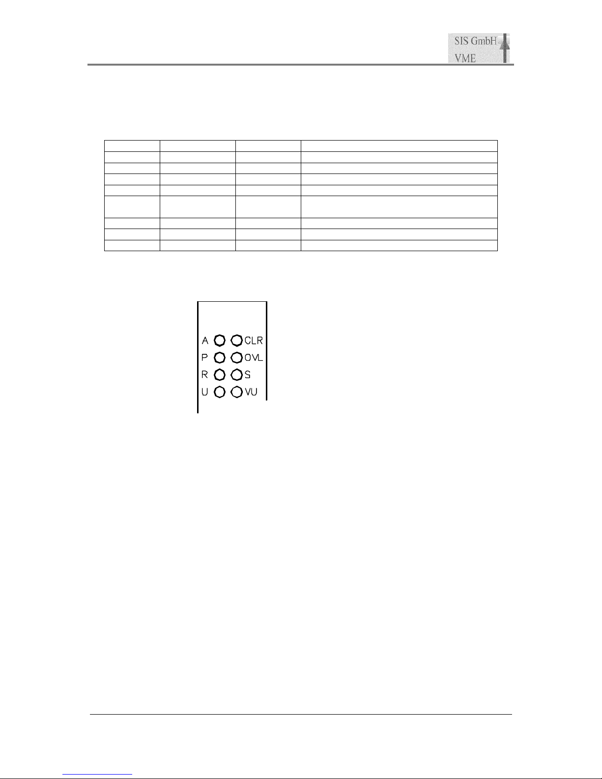
SIS Documentation SIS3820
VME Scaler
Page 53 of 79
9.2 Front Panel LEDs
The SIS3820 has 8 front panel LEDs to visualize part of the units status. Three LEDs
according to the VME64xP standard (Power, Access and Ready) plus 5 additional LEDs
(VME user LED, Clear, Overflow, Scaler enable and VIPA user LED).
Designation LED Color Function
A Access yellow Signals VME access to the unit
P Power red Flags presence of VME power
R Ready green Signals configured logic
U VME user LED green To be switched on/off under user program control
CLR Clear yellow MCS mode: signals LNE
Latching scaler: signals soft or hardware clear
OVL Overflow red Signals Overlow in one or more channels
S Scaler Enable green Signals one or more enabled channels
VU VIPA user LED green for future use
The LED locations are shown in the portion of the front panel drawing below.
The VME Access, Clear and Scaler enable LEDs are monostable (i.e. the duration of the on
phase is stretched for better visibility), the other LEDs reflect the current status.
An LED test cycle is performed upon power up (refer to the chapter 16.6).
Page 54
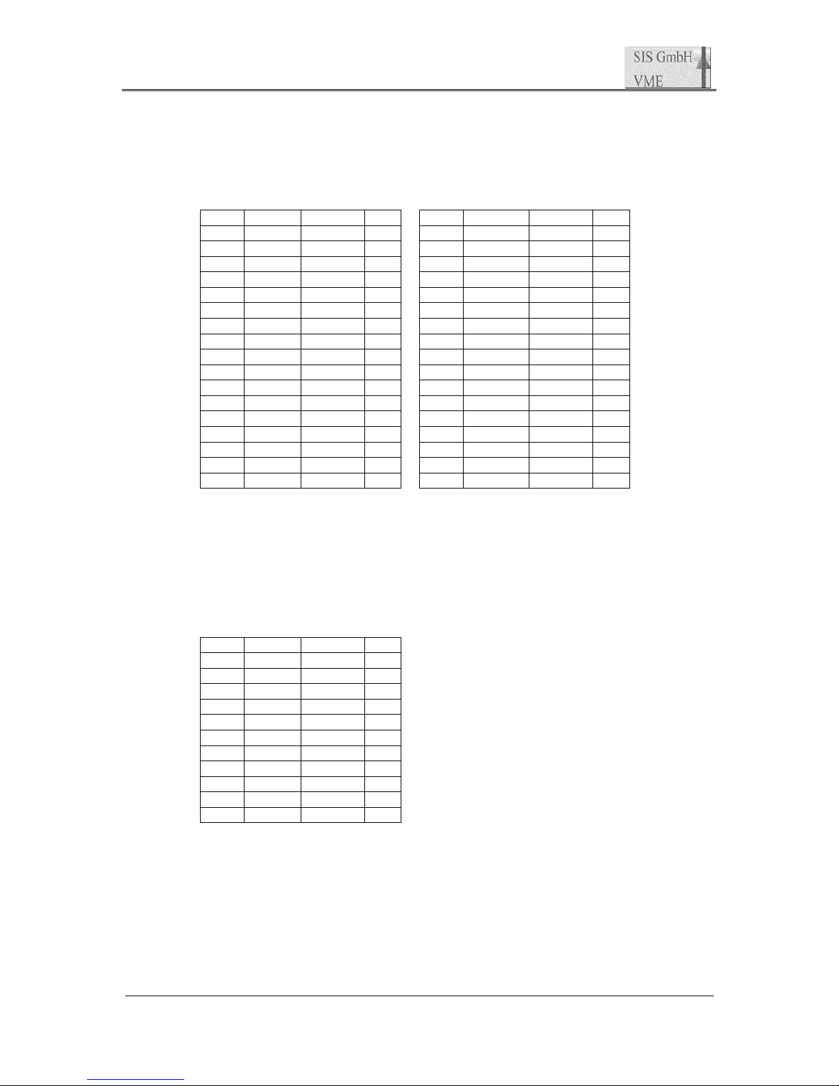
SIS Documentation SIS3820
VME Scaler
Page 54 of 79
9.3 Flat cable Input/Output Pin Assignments
9.3.1 ECL
Data-Connector Channel 1-16 Data-Connector Channel 17-32
PIN SIGNAL SIGNAL PIN PIN SIGNAL SIGNAL PIN
32 IN16 - IN16 + 31 32 IN32 - IN32 + 31
30 IN15 - IN15 + 29 30 IN31 - IN31 + 29
28 IN14 - IN14+ 27 28 IN30 - IN30 + 27
26 IN13 - IN13 + 25 26 IN29 - IN29 + 25
24 IN12 - IN12 + 23 24 IN28 - IN28 + 23
22 IN11 - IN11 + 21 22 IN27 - IN27 + 21
20 IN10 - IN10 + 19 20 IN26 - IN26 + 19
18 IN9 - IN9 + 17 18 IN25 - IN25 + 17
16 IN8 - IN8 + 15 16 IN24 - IN24 + 15
14 IN7 - IN7 + 13 14 IN23 - IN23 + 13
12 IN6 - IN6 + 11 12 IN22 - IN22 + 11
10 IN5 - IN5 + 9 10 IN21 - IN21 + 9
8 IN4 - IN4 + 7 8 IN20 - IN20 + 7
6 IN3 - IN3 + 5 6 IN19 - IN19 + 5
4 IN2 - IN2 + 3 4 IN18 - IN18 + 3
2 IN1 - IN1 + 1 2 IN17 - IN17 + 1
Front view Front view
INx + = ECL High active INx + = ECL High active
INx - = ECL Low active INx - = ECL Low active
Control-Connector Input 1-4 /Output 5-8
PIN SIGNAL SIGNAL PIN
20 GND GND 19
18 OUT8- OUT8+ 17
16 OUT7- OUT7+ 15
14 OUT6- OUT6+ 13
12 OUT5- OUT5+ 11
10 GND GND 9
8 IN4 - IN4 + 7
6 IN3 - IN3 + 5
4 IN2 - IN2 + 3
2 IN1 - IN1 + 1
Front view
INx + = ECL High active
INx - = ECL Low active
OUTx + = ECL High active
OUTx - = ECL Low active
Page 55
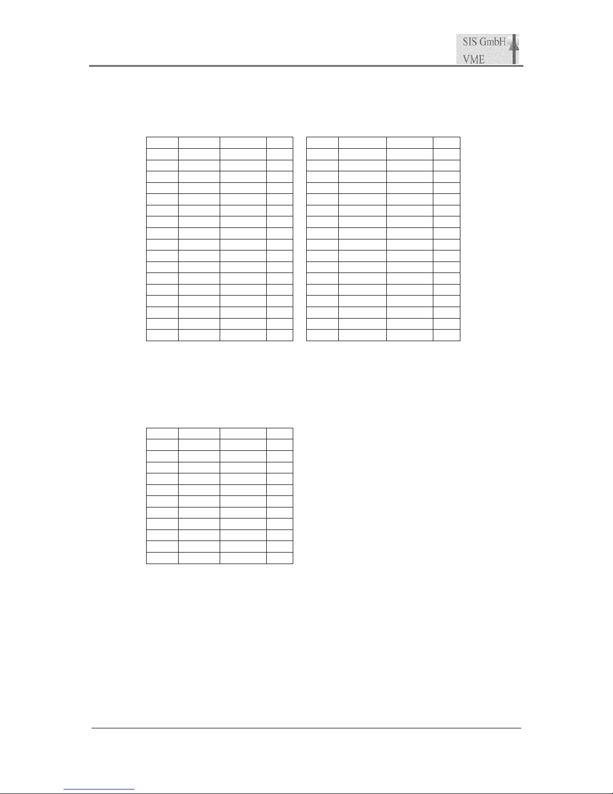
SIS Documentation SIS3820
VME Scaler
Page 55 of 79
9.3.2 TTL
Data-Connector Channel 1-16 Data-Connector Channel 17-32
PIN SIGNAL SIGNAL PIN PIN SIGNAL SIGNAL PIN
32 IN16 - GND 31 32 IN32 - GND 31
30 IN15 - GND 29 30 IN31 - GND 29
28 IN14 - GND 27 28 IN30 - GND 27
26 IN13 - GND 25 26 IN29 - GND 25
24 IN12 - GND 23 24 IN28 - GND 23
22 IN11 - GND 21 22 IN27 - GND 21
20 IN10 - GND 19 20 IN26 - GND 19
18 IN9 - GND 17 18 IN25 - GND 17
16 IN8 - GND 15 16 IN24 - GND 15
14 IN7 - GND 13 14 IN23 - GND 13
12 IN6 - GND 11 12 IN22 - GND 11
10 IN5 - GND 9 10 IN21 - GND 9
8 IN4 - GND 7 8 IN20 - GND 7
6 IN3 - GND 5 6 IN19 - GND 5
4 IN2 - GND 3 4 IN18 - GND 3
2 IN1 - GND 1 2 IN17 - GND 1
Front view Front view
INx - = TTL Low active (74F245) INx - = TTL Low active (74F245)
Control-Connector Input 1-4 /Output 5-8
PIN SIGNAL SIGNAL PIN
20 GND GND 19
18 OUT8- GND 17
16 OUT7- GND 15
14 OUT6- GND 13
12 OUT5- GND 11
10 GND GND 9
8 IN4 - GND 7
6 IN3 - GND 5
4 IN2 - GND 3
2 IN1 - GND 1
Front view
INx - = TTL Low active (74F245)
OUTx - = TTL Low active (74F244)
Page 56
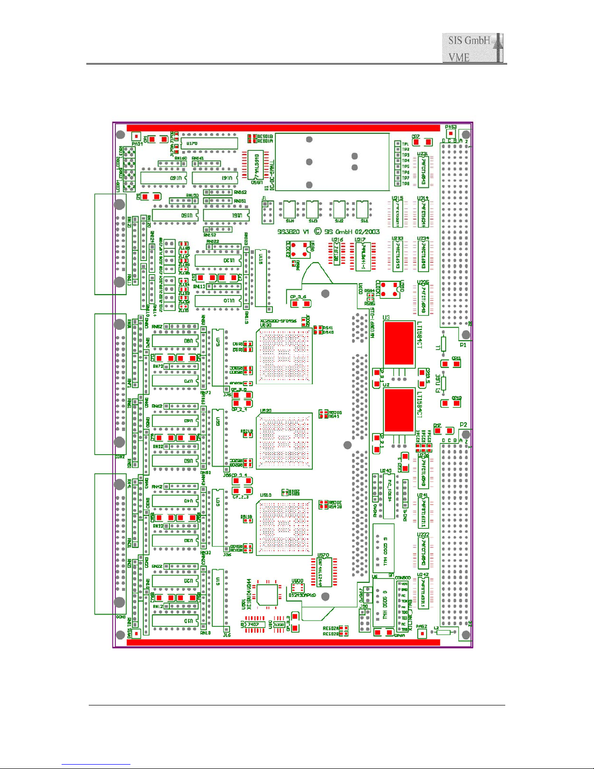
SIS Documentation SIS3820
VME Scaler
Page 56 of 79
10 Board Layout
Find below a printout of the top assembly drawing.
Page 57

SIS Documentation SIS3820
VME Scaler
Page 57 of 79
11 Jumper settings/pinouts
The SIS3820 has 3 jumper fields and a JTAG connector.
Jumper field Function
J1 VME addressing mode
J90 Reset behavior
JP570 JTAG source
CON500 JTAG connector
The first pin of the jumper fields is marked by a square pin on the solder side and an extra
frame on the silk screen of the component side.
11.1 J1
J1 is in charge of the VME addressing mode and SDRAM size selection. At this point in time
the user can select between rotary switch selected A32 addressing and geographical A32
addressing.. A closed position selects the corresponding function.
Function
EN_A32
reserved
EN_GEO
J1
SDRAM
The default setting for a 64 MB unit is EN_A32 closed and all other positions opened.
Following memory architectures are supported
Memory size rows columns banks
64 MB 12 9 1
512 MB 13 10 2
Note: An example to determine the architecture from the SPD can be found in the Visual C++
example sis3820_sdram_eeprom.c
11.2 J90
J90 controls the reset behavior of the SIS3820.
Function
reserved
connect VME reset to SIS3820 reset
reserved
J90
enable watchdog
The default setting is VME reset and enable watchdog closed and all other positions opened.
Note: open the enable watchdog for firmware upgrades
Page 58
SIS Documentation SIS3820
VME Scaler
Page 58 of 79
11.3 JP570 JTAG source
Firmware can be loaded to the XC18V04 serial PROM via a JTAG download cable (XILINX
JTAG-PC4 e.g.) or via the VME interface of the SIS3830. Please note, that errors during this
process can render a module temporarily in non working condition.. JP570 has 3 pins.
Depending on whether pins 1 and 2 or 2 and 3 are closed the JTAG source is defined as listed
below.
Closed JTAG source
1-2 JTAG connector CON 500
2-3 VME
Note: shipping default is 1-2 closed (i.e. JTAG over CON500)
11.4 CON500 JTAG
The SIS3820 on board logic can load its firmware from a serial PROMs . The firmware can
be upgraded through VME (future option) or the JTAG connector. A list of firmware designs
can be found under http://www.struck.de/sis3820firm.htm.
Hardware like the XILINX HW-JTAG-PC in connection with the appropriate software (the
XILINX WebPACK is furnished on the accompanying CDROM) will be required for in field
JTAG firmware upgrades through the JTAG connector.
The JTAG connector is a 9 pin single row 1/10 inch header, the pin assignment on the
connector can be found in the table below.
Pin Short hand Description
1 VCC Supply voltage
2 GND Ground
3 nc not connected, cut to avoid polarity mismatch
4 TCK test clock
5 nc not connected
6 TDO test data out
7 TDI test data in
8 nc not connected
9 TMS test modus
Note: close the J90 disable watchdog jumper for firmware upgrades
Page 59

SIS Documentation SIS3820
VME Scaler
Page 59 of 79
12 Input Configuration
SIS36/38xx boards are available for NIM, TTL , ECL and LVDS input levels and in LEMO
and flat cable versions. The boards are factory configured for the specified input level and
connector type. Input termination is installed.
12.1 ECL
The 100 Ω input termination can be removed in groups of four channels by removing the
corresponding resistor networks. The termination of single control inputs can be disabled with
jumpers J101 through J108, an open jumper disables the termination of the corresponding
channel.
Network Channels 1 K Networks
RN10 1-4 RN11/12
RN20 5-8 RN21/22
RN30 9-12 RN31/32
RN40 13-16 RN41/41
RN50 17-20 RN51/52
RN60 21-24 RN61/62
RN70 25-28 RN71/72
RN80 29-32 RN81/82
RN110 Control 1-4 RN111/RN112
RN120 Control 5-8 RN121/RN122
The schematics of the ECL input circuitry is shown below.
-
+
+
-
-5 V
GND
1 K
1 K
100SIL RN(1)X0
SIL RN(1)X1
SIL RN(1)X2
Page 60
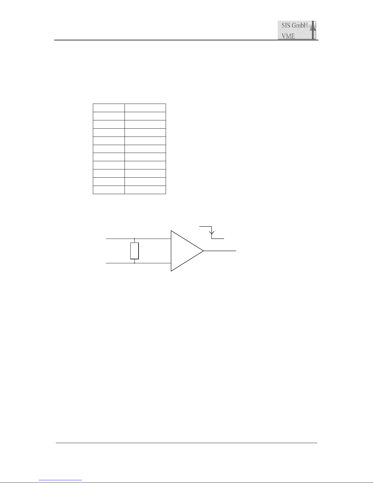
SIS Documentation SIS3820
VME Scaler
Page 60 of 79
12.2 LVDS
The 100 Ω input termination can be removed in groups of four channels by removing the
corresponding resistor networks. The termination of single control inputs can be disabled with
jumpers J101 through J108, an open jumper disables the termination of the corresponding
channel.
Network Channels
RN10 1-4
RN20 5-8
RN30 9-12
RN40 13-16
RN50 17-20
RN60 21-24
RN70 25-28
RN80 29-32
RN110 Control 1-4
RN120 Control 5-8
The schematics of the LVDS input circuitry is shown below.
-
+
-
+
100SIL RN(1)X0
Page 61
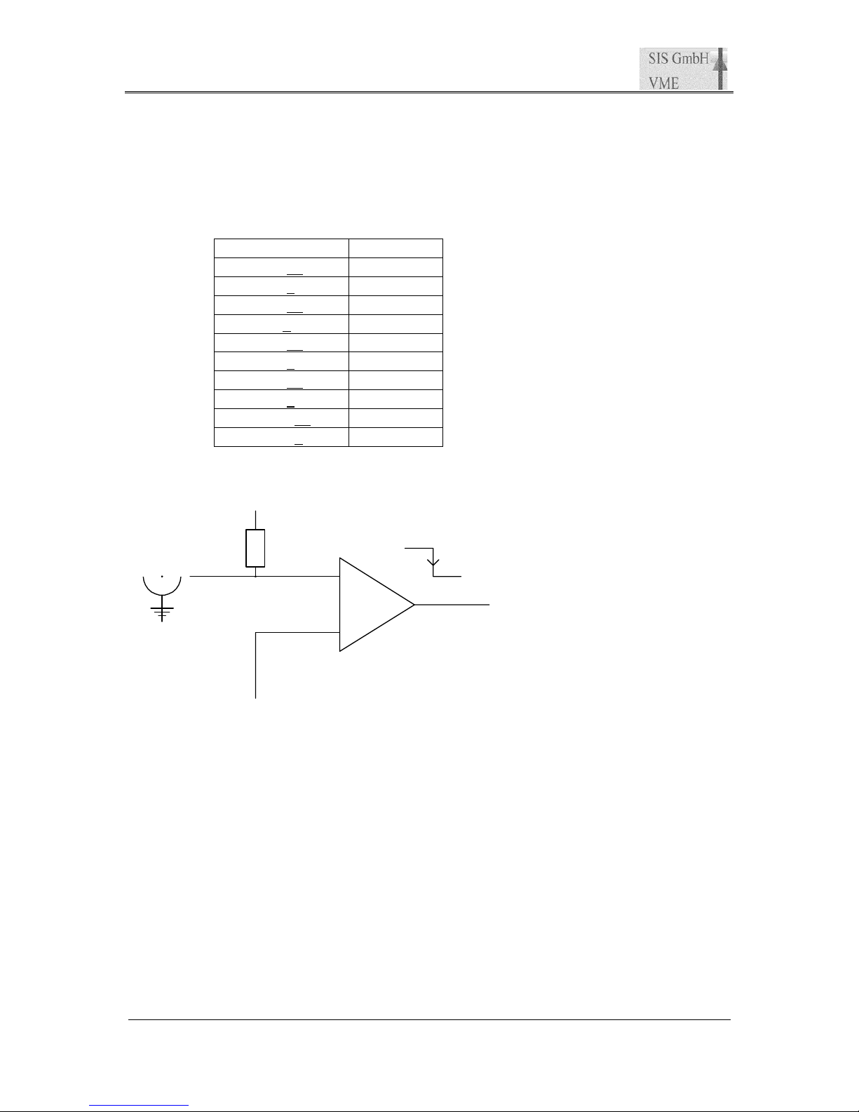
SIS Documentation SIS3820
VME Scaler
Page 61 of 79
12.3 NIM
The 50 Ω input termination can be removed in groups of four channels by removing the
corresponding resistor networks. The termination of single control inputs can be disabled with
jumpers J101 through J108, an open jumper disables the termination of the corresponding
channel.
Network Channels
U15 (Pins 10 to 6) 1-4
U15 (Pins 1 to 5) 5-8
U35 (Pins 10 to 6) 9-12
U35(Pins 1 to 5) 13-16
U55 (Pins 10 to 6) 17-20
U55 (Pins 1 to 5) 21-24
U75 (Pins 10 to 6) 25-28
U75 (Pins 1 to 5) 29-32
U115 (Pins 10 to 6) Control 1-4
U115 (Pins 1 to 5) Control 5-8
The schematics of the NIM input circuitry is shown below.
+
-
Ref=-0.35 V
GND
50
Page 62
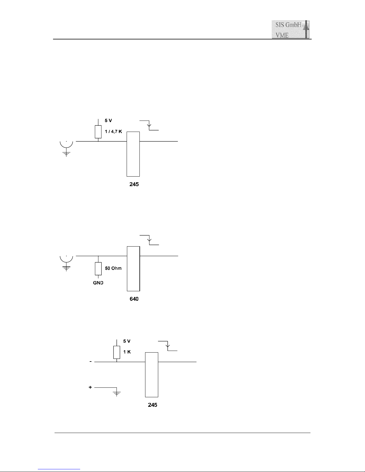
SIS Documentation SIS3820
VME Scaler
Page 62 of 79
12.4 TTL
The TTL input level option is possible with LEMO and flat cable connectors.
12.4.1 High impedance TTL/LEMO
The (low active) TTL/LEMO input circuitry is sketched below. 1 KΩ and 4,7 KΩ termination
are available as options. A high active version can be implemented by replacing the 74F245
with a 74F640
12.4.2 50Ω TTL/LEMO
The (high active) TTL/LEMO 50 Ω input impedance circuitry is shown below.
12.4.3 TTL/Flat Cable
In the flat cable TTL version the positive (right hand side) of the connector is tied to ground.
Page 63

SIS Documentation SIS3820
VME Scaler
Page 63 of 79
13 TTL output configuration
Standard TTL units drive high impedance signals (i.e. 24 mA current), a 50 Ω driver piggy
(driving 48 mA) pack is installed on 50 Ω TTL units. It plugs into the socket U170 instead of
the standard driver chip.
14 Signal Specification
14.1 Control Signals
The width of clear and external next pulses has to be greater or equal 10 ns, an external inhibit
(disable counting) has to be present for the period you desire to disable counting. An internal
delay of some 15 ns has to be taken into account for all external signals.
14.2 Inputs
The SIS3820 is specified for counting rates of 250 MHz for ECL and NIM signals and 100
MHz for the TTL case. Thus the minimum high and low level duration is 2.0 ns (5 ns
respective). Signal deterioration over long cables has to be taken into account.
14.3 User Bits
The status of the user bits is latched with the leading edge of the external LNE pulse. A setup
time of greater equal 10 ns and a hold time of 25 ns is required, i.e. the signal should have a
length of greater 35 ns and has to be valid 10 ns before the leading edge of the LNE pulse
arrives. User bit information is pipelined, i.e. the information that is stored with the scaler
values was recorded at the beginning of the counting period.
Page 64
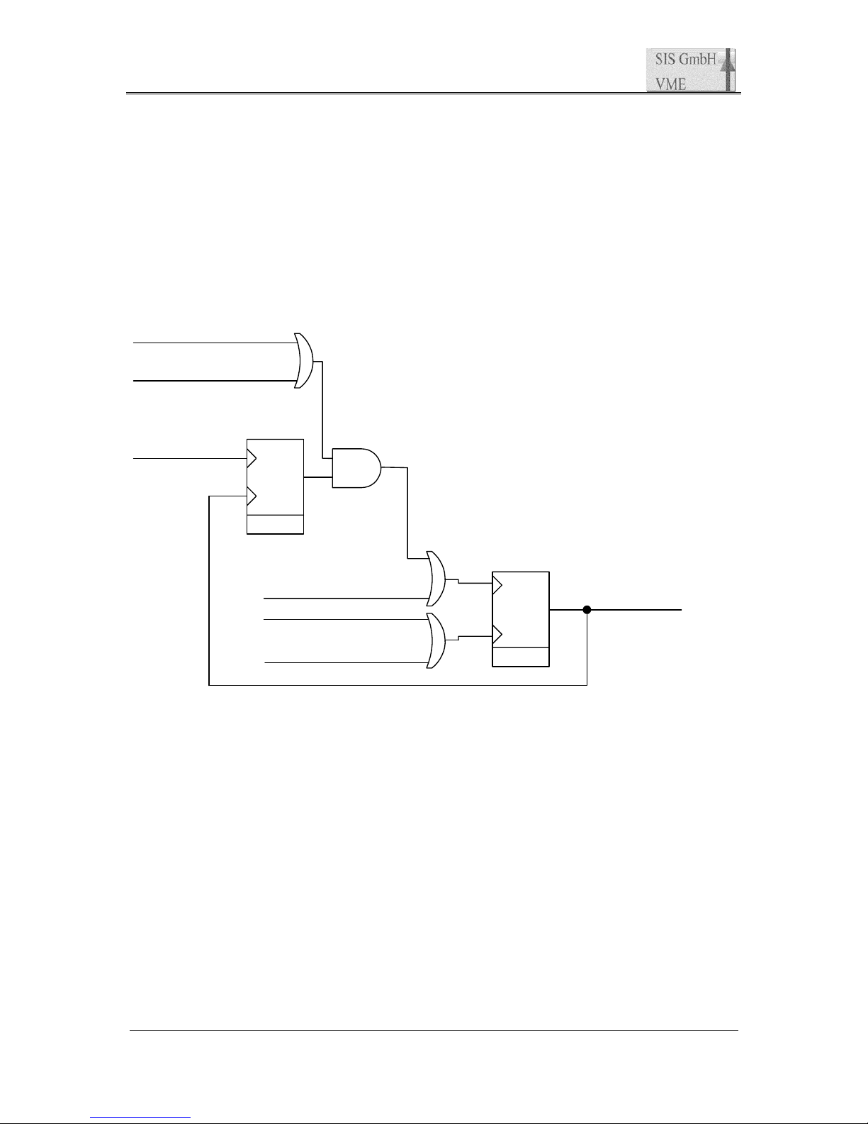
SIS Documentation SIS3820
VME Scaler
Page 64 of 79
15 Theory of operation
15.1 Enable Logic
The logic of the SIS3820 is disabled by default upon power up of the module (due to the
execution of a key reset). In a standard counter application a key enable command is all that is
required to enable the logic, in MCS or preset mode other signals like arm and LNE are
contributing as shown in the enable logic schematic below.
The enable logic should not be mixed with the counter enable/disable for the individual
channels.
SET
Clear
Enable
SET
Clear
ARM
Enable
Key ARM
O
R
Acq Preset
Key Reset
Key Enable
O
R
CHN (enabled, selected)
LNE (enabled, mode 1,2,3)
AND
O
R
Page 65

SIS Documentation SIS3820
VME Scaler
Page 65 of 79
15.2 Read on the fly
The SIS3820 supports read on the fly (i.e. readout in parallel to the acquisition of new counts)
with an accuracy down to the lowest bit at the full counting rate of 200 MHz. While the
uncertainty on a read on the fly is one count no counts are lost. A read from a counter register
of the SIS3820 initiates a clock shadow transaction and the actual counter value that is read
from VME is taken from the shadow register. The counter values of all 32 scaler channels are
latched to the shadow registers simultaneously when the read on the fly is done in BLT32.
Minimum difference in time (i.e. less than 5 ns variation) of the read values can be achieved
with this mechanism.
15.3 Latching scaler
Counter data can be copied to the shadow registers in three ways
• Key VME LNE/clock shadow
• external next pulse LNE/clock shadow with input modes 1, 2 and 3
• read from the counter registers
Shadow register data are not altered/updated in the normal counting process, i.e. the latched
values can be re/read until they are overwritten by the next clock shadow cycle.
15.4 Preset Scaling
In preset mode the counting mode is started by an enable command and stopped by a channel
reaching the preset value of counts. The preset reached state can be used as interrupt source.
As an alternative you can poll on the preset reached bit in the preset enable and hit register to
check on the occurrence of the preset reached condition.. Preset scaling can be used as LNE
source in multi channel scaling (channel N mode) also.
It will take in the order of 100 ns after the preset condition was detected before the counters
will stop counting. This implies, that the actual stored counter value will be greater than the
preset value for frequencies in excess of some 10 MHz.
Page 66
SIS Documentation SIS3820
VME Scaler
Page 66 of 79
15.5 Multiscaling (MCS)
Multi channel or multiscaling is a method to decouple the realtime behavior of fast counting
processes from the VME readout process. Data are buffered in an onboard memory and
readout at a later point in time in an asynchronous fashion. The SIS3820 uses standard 168pin SDRAM memory strips as buffer, the default size is 64 MBytes. The memory can be used
in:
• SDRAM mode
• FIFO mode
While SDRAM mode fits applications with a known number of acquisition cycles that will fit
into the SDRAM strip completely, FIFO mode allows for the sustained acquisition of
measurements of an arbitrary number of readout cycles under the assumption, that the VME
master is capable of digesting the generated data rate. The time slices (or load next
event=LNE cycles) can be defined by following processes:
• VME LNE
• external LNE signal
• internal 10 MHz pulse generator
• channel N as preset scaler
The later three can be routed through a prescaler.
15.5.1 Minimum dwell time
Find below a table with minimum dwell times for a number of configurations.
Number of channels Channel depth (bits) Dwell time in ns
32 32 960
16 32 500
8 32 340
32 16 660
16 16 340
8 16 260
32 8 500
16 8 260
8 8 220
Please note that a depth of 8 bits (i.e. 0-255 counts) is by far sufficient to hold all counts that
can occur at the maximum count rate and minimum dwell time. The minimum dwell time for
a given configuration can be measured on the CIP output (with output mode 1 and 2).
Page 67

SIS Documentation SIS3820
VME Scaler
Page 67 of 79
15.5.2 arm/enable with MCS
15.5.2.1 enable
Use the key operation enable command for multiscaling with an internal time base (prescaled
internal 10 MHz pulse generator e.g. like in the sis3820_mcs example program). The first
time slice (counting period) will have the same length as consecutive slices this way.
15.5.2.2 arm
Use the key operation arm command for multiscaling with an external time base (LNE
source). By means of the arm/enable source bits of the operation mode register you can define
whether the actual enable will be defined by the LNE front panel signal (with input mode 1,2
or 3 active) or the ChN source. This way your first time slice/counting period will have the
same lengths (angular encoder clock ticks, stepper motor ticks, ...) as consecutive bins.
15.6 Clearing/non clearing mode
The SIS3820 has two sets of counters. The two sets are the actual counters and the „old
counters“. Both counter sets are preset to 0 after a power up/key reset or counter clear.
The actual counter set becomes active with the count enable.
At LNE (or read shadow) following process is initiated depending on the non clearing mode
bit of the acquisition/operation mode register
“non clearing mode” = 0 :
• the contents of the current counter set is subtracted from the contents of the “old
counter” set (which was latched by the previous LNE/clock shadow) and the
difference is stored in the shadow register set or copied to SDRAM/FIFO
• the contents of the current counter set is stored to the “old counter” set
“non clearing mode” = 1 :
• the contents of the current counter set is stored to the shadow register set or copied
to SDRAM/FIFO
Page 68

SIS Documentation SIS3820
VME Scaler
Page 68 of 79
15.7 Histogramming Scaler (HISCAL)
Histogramming scalers are typically used for repetitive low count rate applications. While the
VME master has to readout the data across the VME bus in MCS mode, counts from
consecutive scans are added up on board the SIS3820 in HISCAL operation.
HISCAL operation is the combination of MCS mode with SDRAM add mode. The
HISCAL_START signal is used in addition to the MCS setup. The HISCAL_START signal
(from VME or as a front panel input, as defined with the HISCAL_START_SOURCE_BIT of
the operation mode register) resets the memory pointer to the beginning of the histogram
(until the HISCAL_START_PRESET value is reached or HISCAL operation is disabled.
Refer to the 3 histogramming scaler Visual C++ examples to get started.
15.7.1 Minimum dwell time in HISCAL mode
Find below a table with minimum dwell times for 2 configurations in HISCAL mode.
Number of channels Channel depth (bits) Dwell time in ns
32 32 4000
... ... ...
4 32 500
Note: High word count block transfer access to the SDRAM in parallel to MCS/HISCAL
acquisition can result in an increased worst case minimum dwell time of some 8 µs.
15.8 Firmware upgrade over VME
SIS3820 units at firmware greater or equal 0102 support firmware upgrade over the VME
bus. The VME to JTAG interface is implemented through the JTAG_TEST/JTAG_DATA_IN
and the JTAG_CONTROL registers. Refer to the documentation for the XILINX XC18V04
serial PROM for operation details.
The LINUX and Visual C++ sis3820_jtag_prom.c code on the CDROM allows you to
upgrade the firmware of your SIS3820 in combination with the SIS1100/3100 PCI to VME
interface or to port the code to your VME environment.
Note 1: select the proper JP570 jumper setting to activate JTAG over VME
Note 2: A SIS3820 module may be rendered in non working condition after an error in the
firmware download sequence. Operation/proper firmware has to be re-established with a
JTAG firmware download cable in that case.
Page 69
SIS Documentation SIS3820
VME Scaler
Page 69 of 79
15.9 CBLT readout (3820 01 03 and higher design)
CBLT is a method to speed up the readout of small amounts of data from a larger number of
slaves in conjunction with long setup time masters. As header and trailer words are added in
CBLT, this readout approach is less efficient than low setup overhead list sequencer readout
of masters like the SIS3100 VME sequencer.
Modules which are supposed to participate in a CBLT have to get the same CBLT address, in
the case of the SIS3820 the CBLT address is defined by the upper 8 bits of the CBLT setup
register . The module closest to the CPU has to be defined as “First” CBLT module, the
module at the end of the chain is defined as “Last” CBLT module. All modules have to have
their CBLT enable bit set, the modules must occupy a contiguous set of VME slots as shown
in the sketch below. The token is passed from the previous module to the next module via the
IRQ daisy chain lines as soon as all data have been read. The last module in the chain
terminates the transfer with a VME bus error (BERR). .
VME Crate
CPU
First
Last
Middle
Middle
Schematic CBLT setup
The SIS3820 supports the CBLT readout mode only in the MCS (Multiscaler) mode in FIFO
mode !
Page 70
SIS Documentation SIS3820
VME Scaler
Page 70 of 79
15.9.1 CBLT Setup example
Assume four SIS3820 (as shown in the crate above) are supposed to participate in a CBLT.
The modules are set to D32 addressing and VME base address configuration as shown in the
table below. 0x45 is used as CBLT address and the CBLT setup registers of the four modules
are configured as shown in the list.
Module
number
D32 base address VME slot CBLT setup register Comment
1 0x20000000 11 0x45200805 First, Geo 1, max. 32 words, CBLT enable
2 0x21000000 12 0x45201001 CBLT enable, Geo 2, max. 32 words
4 0x22000000 13 0x45201801 CBLT enable, Geo 3, max. 32 words
4 0x23000000 14 0x45202003 Last, Geo 4, max. 32 words, CBLT enable
0x45200805: CBLT address is 0x45xxxxxx
0x45200805: CBLT Max. Readout Length is 32 (0x20) D32 words (0x80 bytes)
0x45200805: CBLT Geo address is 1
0x45200805: CBLT is enabled and First module in chain
A BLT32 read from VME address 0x45000000 will result in a CBLT over the 4 modules,
with the selected geographical addresses showing up in the header and trailer words.
32-bit data word Content Comment
1 0x08000000 Header module 1, Geo 1
2 Value ch. 1, module 1
.. ..
33 Value ch. 32, module 1
34 0x08000088 Trailer module 1, 0x88 Bytes
35 0x10000000 Header module 2, Geo 2
36 Value ch. 1, module 2
.. ..
67 Value ch. 32, module 2
68 0x10000088 Trailer module 2, 0x88 Bytes
69 0x18000000 Header module 3, Geo 3
70 Value ch. 1, module 3
.. ..
101 Value ch. 32, module 3
102 0x18000088 Trailer module 3, 0x88 Bytes
103 0x20000000 Header module 4, Geo 4
104 Value ch. 1, module 4
.. ..
135 Value ch. 32, module 4
136 0x21000088 Trailer module 4, 0x88 Bytes,
Status: Last module (bit 24)
Page 71
SIS Documentation SIS3820
VME Scaler
Page 71 of 79
If the modules contain no scaler data (FIFO is empty), the resulting VME data will look like
shown below.
32-bit data word Content Comment
1 0x08000000 Header module 1, Geo 1
2 0x08000008 Trailer module 1, 8 Bytes
3 0x10000000 Header module 2, Geo 2
4 0x10000008 Trailer module 2, 8 Bytes
5 0x18000000 Header module 3, Geo 3
6 0x18000008 Trailer module 3, 8 Bytes
7 0x20000000 Header module 4, Geo 4
8 0x21000008 Trailer module 4, Status: Last module, 8 Bytes
15.9.2 CBLT hints
While it is trivial to setup a block of modules for CBLT readout, one has to be aware of
specialities of this readout form.
• The user has to make sure, that the read access to the CBLT address is a BLT32 block
transfer (with address modifier AM=0xB or AM=0xF), i.e. the modules will not respond
to a read, which is broken down into many single reads (AM 0x9 e.g.). This can be
verified with a VME diagnosis module like the VDIS or with an oscilloscope and an
extender.
• The requested number of bytes of the CBLT transfer have to be higher than the max.
number of bytes of the readout data of all participated modules. This ensures that the Last
module terminates the CBLT transfer with a BERR* signal. All other participated
modules monitor a BERR* occurring and then they terminate the CBLT transfer. All
modules are now ready for the next event.
• In many cases the block size will not be known, as it may depend on the number of hits in
an ADC or TDC. In that case the user will have to setup a CBLT with the number of
possible words and rely on the capability of a block transfer terminated by a VME bus
error and a returned Byte count to indicate the actual length of the transfer.
15.10 Broadcast
Broadcast is a way to distribute a signal like LNE with minimum jitter and latency to a
number of SIS3820 units over VME. Broadcast uses the same setup as CBLT. Broadcast
addressing uses the CBLT address plus the offset of the given key address to invoke the
corresponding action. An example will be made available shortly.
Page 72

SIS Documentation SIS3820
VME Scaler
Page 72 of 79
16 Appendix
16.1 P2 row A/C pin assignments
The P2 connector of the SIS3820 (in 64 channel or clock module configuration) has
connections on rows A and C to feed the second set of 32 inputs to the module or for
operation as backplane clock distributor for the SIS330x digitizer family. This implies, that
the module can not be operated in a VME slot with a special A/C backplane, like VSB e.g..
The pin assignments of P2 rows A/C of the SIS3820 for both scaler and clock module is
shown below. 32 channel versions do not make use of P2 rows A/C.
P2A Scaler Function Clock Function P2C Scaler Function Clock Function
1 not connected -5.2 V 1 not connected -5.2 V
2 not connected -5.2 V 2 not connected -5.2 V
3 not connected -5.2 V 3 not connected -5.2 V
4 not connected not connected 4 not connected not connected
5 not connected not connected 5 not connected not connected
6 DGND DGND 6 DGND DGND
7 Control 1 P2_CLOCK_H 7 Control 0 P2_CLOCK_L
8 DGND DGND 8 DGND DGND
9 Control 3 P2_START_H 9 Control 2 P2_START_L
10 Control 5 P2_STOP_H 10 Control 4 P2_STOP_L
11 Control 7 P2_TEST_H 11 Control 6 P2_TEST_L
12 DGND DGND 12 DGND DGND
13 DGND DGND 13 DGND DGND
14 G34_L16 not connected 14 G34_L15 not connected
15 G34_L14 not connected 15 G34_L13 not connected
16 G34_L12 not connected 16 G34_L12 not connected
17 G34_L10 not connected 17 G34_L9 not connected
18 G34_L8 not connected 18 G34_L7 not connected
19 G34_L6 not connected 19 G34_L5 not connected
20 G34_L4 not connected 20 G34_L3 not connected
21 G34_L2 not connected 21 G34_L1 not connected
22 DGND DGND 22 DGND DGND
23 G12_L16 not connected 23 G12_L15 not connected
24 G12_L14 not connected 24 G12_L13 not connected
25 G12_L12 not connected 25 G12_L11 not connected
26 G12_L10 not connected 26 G12_L9 not connected
27 G12_L8 not connected 27 G12_L7 not connected
28 G12_L6 not connected 28 G12_L5 not connected
29 G12_L4 not connected 29 G12_L3 not connected
30 G12_L2 not connected 30 G12_L1 not connected
31 DGND DGND 31 DGND DGND
32 not connected not connected 32 not connected not connected
Page 73
SIS Documentation SIS3820
VME Scaler
Page 73 of 79
16.2 Row d and z Pin Assignments
The SIS3820 is ready for the use with VME64x and VME64xP backplanes. Features include
geographical addressing (PCB revisions V2 and higher) and live insertion (hot swap). The
used pins on the d and z rows of the P1 and P2 connectors are listed below.
Position P1/J1 P2/J2
Row z Row d Row z Row d
1 VPC (1)
2 GND GND (1) GND
3
4 GND GND
5
6 GND GND
7
8 GND GND
9 GAP*
10 GND GA0* GND
11 RESP* GA1*
12 GND GND
13 GA2*
14 GND GND
15 GA3*
16 GND GND
17 GA4*
18 GND GND
19
20 GND GND
21
22 GND GND
23
24 GND GND
25
26 GND GND
27
28 GND GND
29
30 GND GND
31 GND (1) GND (1)
32 GND VPC (1) GND VPC (1)
Note: Pins designated with (1) are so called MFBL (mate first-break last) pins on the installed 160 pin
connectors, VPC(1) pins are connected via inductors.
Page 74
SIS Documentation SIS3820
VME Scaler
Page 74 of 79
16.3 Connector Types
Find below a list of connector types that are used on the SIS3820.
Connector Purpose Part Number
160 pin zabcd VME P1/P2 Harting 02 01 160 2101
20 pin header Control (flat cable versions) DIN41651 20 Pin (AMP e.g.)
34 pin header Inputs (flat cable versions) DIN41651 34 Pin (AMP e.g.)
LEMO Control and Input (LEMO versions) LEMO ERN.00.250.CTL
SDRAM SDRAM memory socket Berg 88638-60002
16.4 Power consumption
The SIS3820 is a single +5 V supply board. Lower positive voltages (3.3 V and 2.5 V) are
generated with low dropout regulators. –5 V is generated with up to 3 DC/DC converters.
Board type Voltage Current
SIS3820-SCALER (32 ECL channels) 5 V 2,0 A
SIS3820-SCALER (32 TTL channels 5 V 1,3 A
SIS3820-CLOCK (32 NIM channels) 5 V 3,2 A
16.5 Operating conditions
16.5.1 Cooling
Although the SIS3820 is mainly a 2.5 and 3.3 V low power design, forced air flow is required
for the operation of the board. The board may be operated in a non condensing environment at
ambient temperatures between 10° and 40° Celsius.
16.5.2 Hot swap/live insertion
Please note, that the VME standard does not support hot swap by default. The SIS3820 is
configured for hot swap in conjunction with a VME64x backplane. In non VME64x
backplane environments the crate has to be powered down for module insertion and removal.
16.6 LED (selftest)
During power up self test and FPGA configuration all LEDs except the Ready (R) LED are
on. After the initialization phase is completed, all LEDs except the Ready (R) LED and the
Power (P) have to go off. Differing behavior indicates either a problem with the download of
the firmware boot file or one or more FPGAs and/or the download logic.
Page 75
SIS Documentation SIS3820
VME Scaler
Page 75 of 79
16.7 VME readout performance
A SIS3820 can generate in excess of 128 MBytes/s worth of data (at the minimum dwell time
with 32 channels active in 32-bit mode) in principle. A more realistic data rate in the short
dwell time regime is 64 MBytes/s, as 8-bits counter depth will be sufficient to hold the
maximum possible number of counts. The VME interface was optimized with respect to the
block transfer readout of this possible substantial amount of data. Find below a table of block
transfer speeds of the SIS1100/3100 PCI to VME interface on readout of data from the
SDRAM of the SIS3820. The measurements were made with 40 longword blocks (the speed
was computed by dividing the number of bytes be the difference of the leading edge of the
first DS1 and the trailing edge of the last DS1).
Mode Transfer speed
BLT32 25 MB/s
MBLT64 50 MB/s
2e VME 88 MB/s
Note: you have to be aware, that the typical setup time for a block transfer is in the 25 µs
ballpark. I.e. you will want to read out large blocks of data in high speed applications to
minimize overhead.
16.8 Software Support
The SIS3820 board comes with the sis3820.h header file that defines register offsets as well
as relevant bit addresses within the registers. This header file should facilitate SIS3820
software development for all platforms.
C example code for the SIS3820 is provided for both Visual C++ and LINUX. The code was
written to be used with the SIS1100/3100 PCI to VME interface, but should be readily
portable to other environments.
A Windows Labview interface is available for the SIS3150 USB2.0 to VME interface.
Page 76
SIS Documentation SIS3820
VME Scaler
Page 76 of 79
17 Glossary
Following shorthands/expressions are used throughout the manual
Term Explanation
ChN Channel N as LNE source
CIP Copy in progress (data are copied from the frontend FPGA registers to
memory registers on the VME FPGA)
Clock Shadow Initiate copy process of frontend scaler data to register set
FPGA Field Programmable Gate Array
HISCAL Histogramming Scaler
KA Key address. Write access with arbitrary data to a key address initiates the
specified function
LNE Load Next Event. Initiate next counting period, save data from previous
counting period.
MCS Multi Channel Scaler
Page 77

SIS Documentation SIS3820
VME Scaler
Page 77 of 79
18 Index
10 MHz pulser 38
2eVME 8, 10, 30, 75
50 Ohm impedance 62
A24 8
A32 8, 11, 16, 57
ADC 71
address
geographical 70, 71
address map 17
address modifier 71
address space 16
addressing
geographical 8
AM 71
arm 37, 64, 67
arm source 37, 67
backplane 8, 16, 74
bank 50, 57
BERR 49, 69
block diagram 9
BLT32 8, 30, 70, 75
board layout 56
Bonn 22
broadcast 8
Broadcast 71
bus error 18, 69
CBLT 8, 17, 29, 69, 71
hints 71
setup example 70
channel N 38
channel number 50
ChN 67
CIP 27, 76
clock shadow 24, 35, 36, 65
column 57
CON500 58
connector 8
Connector Types 74
cooling 74
counter 10
current counter 67
D32 8, 70
data format 39
Data Format 50
DC/DC 74
DO8 22
driver
50 Ω 63
high impedance 63
DS1 75
DS2430 48
DSP 10
dwell time 10, 40
ECL 54, 59, 63
edge sensitive 24
EEPROM 48
EN_A32 16
EN_GEO 16
enable 67
enable logic 64
enable source 37, 67
FIFO 67
almost full 31
FIFO address space 49
firmware 58, 68
FPGA 74, 76
front panel 8
Front Panel
LED 53
Front Panel Layout 52
GA 16
geographical addressing 73
glossary 76
GND 58
header 70, 71, 75
high impedance 62, 63
HISCAL 33, 35, 37, 68, 76
HISCAL_START 35
HISCAL_START_SOURCE_BIT 36, 68
histogramming scaler 10
hot swap 73, 74
Input Configuration 59
input mode 45
installation 11
Intel 22
interrupt 24
interrupt source 24
interrupt sources 24
interrupter mode 22
interrupter type 22
introduction 7
IRQ
acquisitions reached 25
almost full 25
clock shadow 23, 24
FIFO almost full 23
FIFO threshold 23, 24
LNE 23, 24
overflow 23, 25
preset reached 24
source 24
source 0 24
source 1 24
source 2 24, 26
source 3 25
source 4 25
IRQ mode 22
ROAK 22
RORA 22
J1 16, 57
J90 57, 58
JP570 58, 68
JTAG 9, 57, 58, 68
jumper settings 57
Page 78

SIS Documentation SIS3820
VME Scaler
Page 78 of 79
KA 76
Labview 75
latching scaler 10, 65
LED 53
Access 53
CLR 13
Color 53
power 74
Power 53
ready 74
Ready 53
S 13
selftest 74
user 11, 19
LEMO 74
level sensitive 24
LINUX 22
LINUX example/test code 11
live insertion 73, 74
LNE 10, 26, 35, 63, 65, 67, 71, 76
external rate limit 27, 38
inhibit 35
LNE prescaler 38
LNE source 38
LVDS 60
MBLT64 8, 10, 30, 75
MCS 10, 30, 38, 39, 66, 68
mode
16-bit 51
24-bit 50
32-bit 50
8-bit 51
channel N 41, 42
clearing 39, 67
FIFO 66
FIFO emulation 29, 37, 49
inhibit 45
input 35, 46, 67
latching scaler 53
MCS 13, 25, 26, 40, 53, 64, 68
multiscaler 24
non clearing 25, 39, 67
of operation 34
output 36, 66
output 3 43
preset 64
preset scaler 25
SDRAM 37, 66
SDRAM add 37, 68
mode
counter test 20
mode
25 MHz test pulses 20
modes of operation 34
monostable 53
Multi channel scaler 10
Multiscaling 66
NIM 61, 63
old counter 67
operating conditions 74
output 63
50 MHz 36
CIP 66
copy in progress 66
enabled 36
SDRAM empty 36
SDRAM threshold 36
user 36
overflow 44
P1 73
P2 73
pin assignments 72
PCB 73
Pin Assignments 54
pin header 74
power consumption 74
preset reached 25
preset scaler 10, 14, 38
preset scaling 65
preset scheme 42
PROM 9, 58
read on the fly 65
reference pulser 20
register
acquisition count 13, 26, 33
acquisition mode 34, 41
acquisition preset 13, 25, 26, 27
address pointer 31
CBLT setup 17, 69, 70
CBLT/broadcast setup 29
channel 1/17 bits 33-48 45
control 21
copy disable 40
FIFO threshold 24
FIFO word count threshold 32
FIFO word counter 31, 49
FIFO word counter threshold 32
firmware revision 21
HISCAL_LAST_ACQ_COUNTER 33
HISCAL_START_COUNTER 33
HISCAL_START_PRESET 33
inhibit 44
interrupt configuration 22
interrupt control 22
interrupt control/status 23
JTAG_CONTROL 47
JTAG_DATA_IN 47
JTAG_TEST. 47
LNE channel 41
module Id. 21
module Id. and firmware revision 11
MUX OUTchannel select 43
one wire Id. 48
operation mode 41, 50, 67, 68
overflow 25
overflow 1 44
overflow 2 44
prescaler factor 38
preset channel select 42
preset enable and hit 14, 65
Page 79

SIS Documentation SIS3820
VME Scaler
Page 79 of 79
preset enable mask 10
preset hit 28
preset hit mask 10
preset value 10
preset value counter group 1 28
preset value counter group 2 28
SDRAM page 30, 49
SDRAM_SPD 46
shadow 29, 39, 67
test pulse mask 20, 46
veto external count inhibit 45, 46
word count 31
ROAK 22
RORA 22
rotary switch 16
row 57
SBC 22
scaler 10
SDRAM 9, 39, 67, 74
size 16
SDRAM empty 36
SDRAM threshold 36
side cover 8
Signal Specification 63
Control 63
Inputs 63
SIL 9
SIS1100/3100 11, 75
SIS3100 30
SIS3100-HISCAL 10
SIS3150 75
sis3820.h 11, 75
Software Support 75
SPD 57
SW3 11, 16
SW4 11, 16
TCK 58
TDC 71
TDI 47, 58
TDO 58
Technical Properties/Features 8
termination 59, 60
TMS 47, 58
trailer 70, 71
TTL 55, 62, 63
50Ω impedance 62
flat cable 62
high impedance 62
output 63
Tundra 22
Universe II 22
USB2.0 75
user
bit 1 35, 50
bit 2 35, 50
bits 50, 63
LED 19, 36
output 36
V/F converter 10
VCC 58
VDIS 71
VME 74
access test 11
bus error 71
P1 74
P2 74
readout performance 75
VME addressing 16
VME64x 8, 16, 73, 74
VME64xP 73
VSB 72
watchdog 57
XC18V04 58, 68
XILINX 68
 Loading...