

Page 1

July 2017
DocID030806 Rev 2
1/26
www.st.com
UM2252
User manual
Getting started with the X-NUCLEO-NFC05A1 NFC card reader
expansion board based on ST25R3911B for STM32 Nucleo
Introduction
The X-NUCLEO-NFC05A1 NFC card reader expansion board is used to evaluate functions based on
the ST25R3911B, designed for the expansion of STM32 Nucleo boards.
It is compatible with the Arduino™ UNO R3 connector and can be plugged to any STM32 Nucleo board
together with other expansion boards to evaluate different devices.
It features:
On-board NFC card reader IC: ST25R3911B
47 mm x 34 mm, four turns, 13.56 MHz inductive antenna etched on PCB and associated tuning
circuit
Six general purpose LEDs
ISO 18092 (NFCIP-1) active P2P
ISO 14443A and ISO14443B
ISO 15693
FeliCa™
VHBR
6.8 Mbit/s AFE and PCD to PICC framing
3.4 Mbit/s PICC to PCD framing
Up to 1.4 W output power with differential antenna
Possibility of driving two antennas in single ended configuration
Inductive and capacitive wake-up
Automatic antenna tuning system
Transparent and Stream modes to implement MIFARE™ Classic compliant or other custom
protocols
Page 2
Getting started
UM2252
2/26
DocID030806 Rev 2
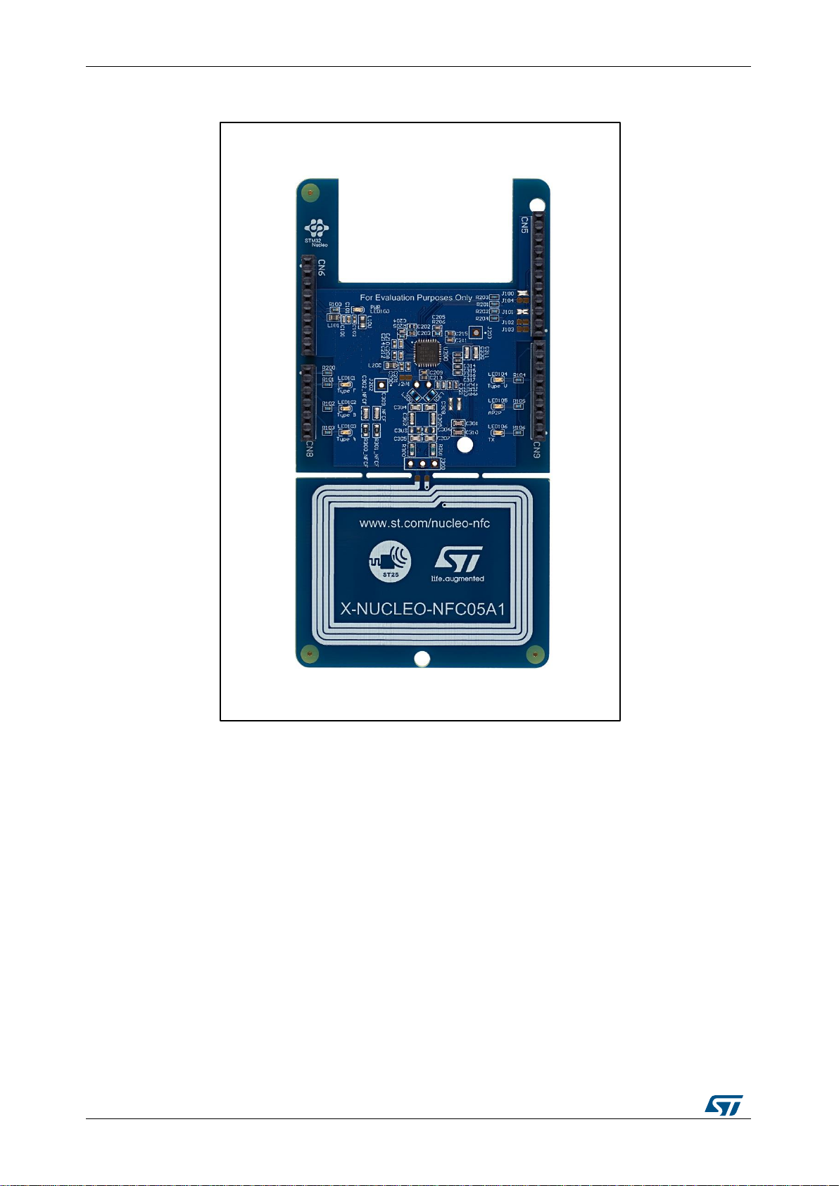
Figure 1: X-NUCLEO-NFC05A1 expansion board
Page 3

UM2252
Contents
DocID030806 Rev 2
3/26
Contents
1 Getting started ................................................................................. 6
1.1 Hardware requirements ..................................................................... 6
1.2 System requirements ........................................................................ 6
2 Board setup ..................................................................................... 7
3 Hardware .......................................................................................... 8
3.1 Host interface and GPIO connection ................................................. 9
3.2 X-NUCLEO-NFC05A1 expansion board component placement ..... 10
4 Component description ................................................................ 11
4.1 ST25R3911B device ....................................................................... 11
4.2 Schematic diagrams ........................................................................ 11
4.2.1 USB connectivity and power supply ................................................. 11
4.2.2 ST25R3911B schematic diagram ..................................................... 13
4.2.3 Antenna and matching network components ................................... 15
4.3 PCB Layout ..................................................................................... 17
4.3.1 PCB layers ........................................................................................ 17
4.3.2 Top layer ........................................................................................... 17
4.3.3 Mid layer 1 ........................................................................................ 18
4.3.4 Mid layer 2 ........................................................................................ 18
4.3.5 Bottom layer ..................................................................................... 19
5 Bill of materials .............................................................................. 20
6 Federal Communications Commission (FCC) and Industry
Canada (IC) compliance ........................................................................ 23
6.1 FCC Compliance Statement............................................................ 23
6.1.1 Part 15.19 ......................................................................................... 23
6.1.2 Part 15.21 ......................................................................................... 23
6.1.3 Part 15.105 ....................................................................................... 23
6.1.4 FCC ID .............................................................................................. 23
6.2 Formal notices required by Industry Canada (“IC”) ......................... 23
6.2.1 Compliance Statement ..................................................................... 23
6.2.2 Declaration de Conformité ................................................................ 23
6.2.3 IC ID.................................................................................................. 24
7 Revision history ............................................................................ 25
Page 4

List of tables
UM2252
4/26
DocID030806 Rev 2
List of tables
Table 1: Interconnections between the X-NUCLEO-NFC05A1 expansion board and the Nucleo-L476RG
board (left side) ........................................................................................................................................... 8
Table 2: Interconnections between the X-NUCLEO-NFC05A1 expansion board and the Nucleo-L476RG
board (right side) ......................................................................................................................................... 8
Table 3: Matching variant ......................................................................................................................... 15
Table 4: X-NUCLEO-NFC05A1 bill of materials ....................................................................................... 20
Table 5: Document revision history .......................................................................................................... 25
Page 5

UM2252
List of figures
DocID030806 Rev 2
5/26
List of figures
Figure 1: X-NUCLEO-NFC05A1 expansion board ..................................................................................... 2
Figure 2: X-NUCLEO-NFC05A1 component placement .......................................................................... 10
Figure 3: STM32 Nucleo connector schematic diagram ........................................................................... 12
Figure 4: ST25R3911B schematic diagram .............................................................................................. 14
Figure 5: Matching circuit schematic diagram .......................................................................................... 16
Figure 6: PCB layout top layer .................................................................................................................. 17
Figure 7: PCB layout mid layer 1 .............................................................................................................. 18
Figure 8: PCB layout mid layer 2 .............................................................................................................. 18
Figure 9: PCB layout bottom layer ............................................................................................................ 19
Page 6

Getting started
UM2252
6/26
DocID030806 Rev 2
1 Getting started
Connect the X-NUCLEO-NFC05A1 to an STM32 Nucleo-64 development board. The PC
USB port has to be capable of delivering at least 300 mA at 5 V supply. A demo software is
available for download at www.st.com to be programmed onto the STM32 Nucleo.
1.1 Hardware requirements
The X-NUCLEO-NFC05A1 expansion board is designed to be used with any STM32
Nucleo board, although complete testing has been performed using the NUCLEO-L476RG
hosting the STM32L476RG microcontroller.
The STM32 Nucleo firmware and the related documentation are available at
http://www.st.com/stm32nucleo.
1.2 System requirements
To use the STM32 Nucleo boards with the X-NUCLEO-NFC05A1 expansion board the
following software and hardware are required:
an STM32 Nucleo-64 development board
a Windows® PC to install the firmware package
a USB type A to Mini-B USB cable to connect the Nucleo board to the PC
unit must be supplied by a safety extra low voltage (SELV) limited power source
through the USB port, the source should not exceed 60Vdc / 8A / 100VA
To install the board firmware package (order code: X-CUBE-NFC5) the PC must have:
128 MB of RAM
40 MB of free hard disk space
The X-CUBE-NFC5 firmware and the related documentation are available at www.st.com.
Page 7

UM2252
Board setup
DocID030806 Rev 2
7/26
1
Connect the X-NUCLEO-NFC05A1 expansion board to the STM32 Nucleo board
from the top through the Arduino® UNO R3 connectors
2
Power the STM32 Nucleo board using a Mini-B USB cable
3
Program the firmware on the STM32 Nucleo board using the provided example
4
Reset the MCU using the reset button available on the STM32 Nucleo board.
The evaluation kit is ready to be used.
2 Board setup
To set up the board;
Page 8
Hardware
UM2252
8/26
DocID030806 Rev 2
Program the microcontroller on the STM32 Nucleo board.
Signal
Connector
Pin number
Nucleo-L476RG
X-NUCLEO-NFC05A1
NC
CN6
Power
1 - -
IOREF 2 -
3V3 (VDD_IO)
RESET 3 -
-
3V3 4 -
3V3 (VDD_IO)
5V 5 -
5V (VDD)
GND 6 -
GND
GND 7 -
GND
VIN 8 -
-
A0
CN8
Analog
1
PA0
IRQ_MCU
A1 2 PA1
MCU_LED1
A2 3 PA4
MCU_LED2
A3 4 PB0
MCU_LED3
A4 5 PC1
-
A5 6 PC0
-
Signal
Connector
Pin number
Nucleo-L476RG
X-NUCLEO-NFC05A1
D15
CN5
Digital
10
PB8
-
D14 9 PB9
-
AVDD 8 AVDD
-
GND 7 GND
GND
D13 6 PA5
CLK_MCU
a
b
3 Hardware
The X-NUCLEO-NFC05A1 expansion board allows the user to test the functionality of the
ST25R3911B ICa, which supports the reader/writer modeb.
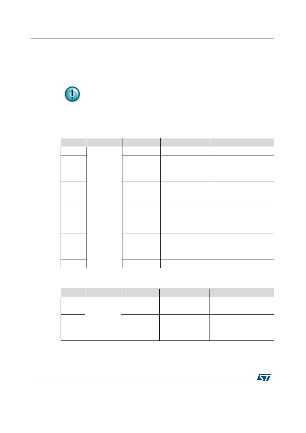
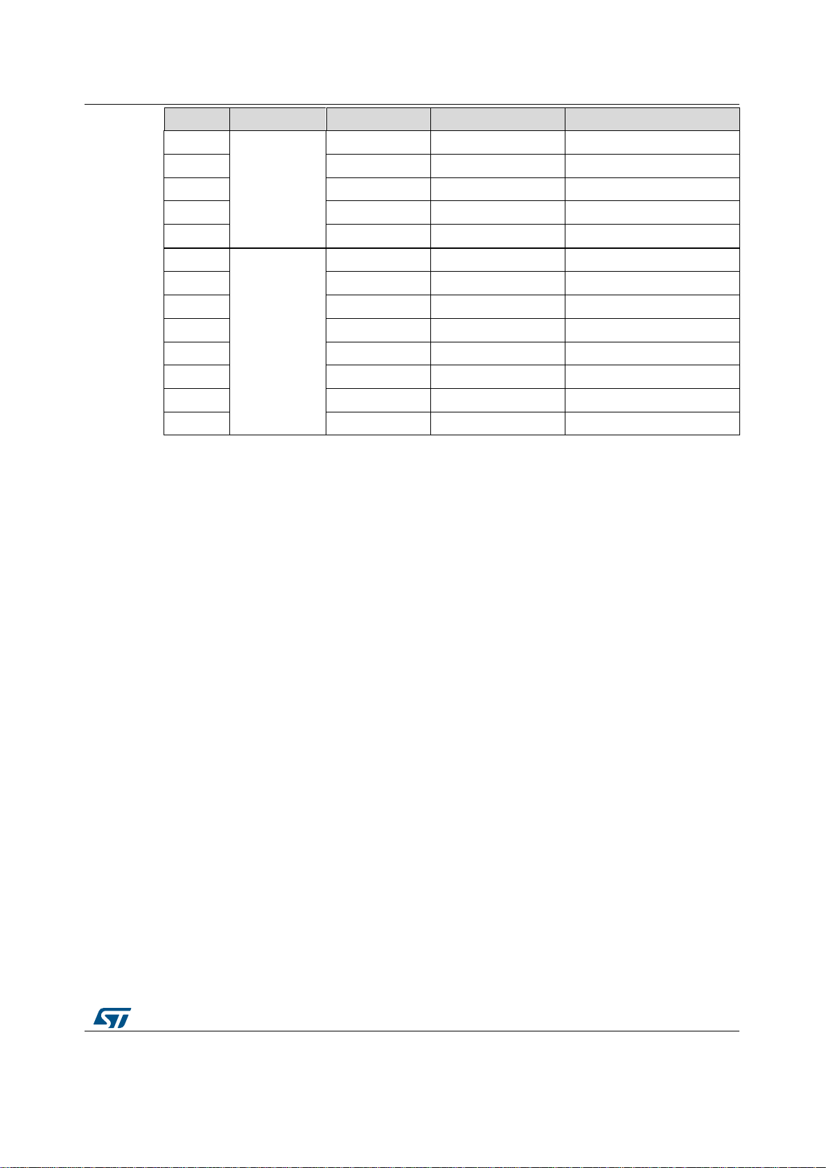
The ST25R3911B IC module and the STM32 Nucleo board are connected through CN5,
CN6, CN8 and CN9 connectors (see the tables below).
Table 1: Interconnections between the X-NUCLEO-NFC05A1 expansion board and the Nucleo-
L476RG board (left side)
Table 2: Interconnections between the X-NUCLEO-NFC05A1 expansion board and the Nucleo-
For the chip complete feature list refer to the ST25R3911B datasheet.
For further details on the supported features, refer to this user manual introduction.
L476RG board (right side)
Page 9
UM2252
Hardware
DocID030806 Rev 2
9/26
Signal
Connector
Pin number
Nucleo-L476RG
X-NUCLEO-NFC05A1
D12 5 PA6
MISO_MCU
D11 4 PA7
MOSI_MCU
D10 3 PB6
/SS_MCU
D9 2 PC7
-
D8 1 PA9
-
D7
CN9
Digital
8
PA8
MCU_LED6
D6 7 PB10
-
D5 6 PB4
MCU_LED4
D4 5 PB5
MCU_LED5
D3 4 PB3
-
D2 3 PA10
-
D1 2 PA2
-
D0 1 PA3
-
3.1 Host interface and GPIO connection
The X-NUCLEO-NFC05A1 expansion board contains the ST25R3911B-AQFT chip and is
powered by the STM32 Nucleo board.
The ST25R3911B is driven by the microcontroller via SPI interface.
The six LEDs indicate the detected technology (for example ISO14443 Type A).
Page 10
Hardware
UM2252
10/26
DocID030806 Rev 2
3.2 X-NUCLEO-NFC05A1 expansion board component
placement
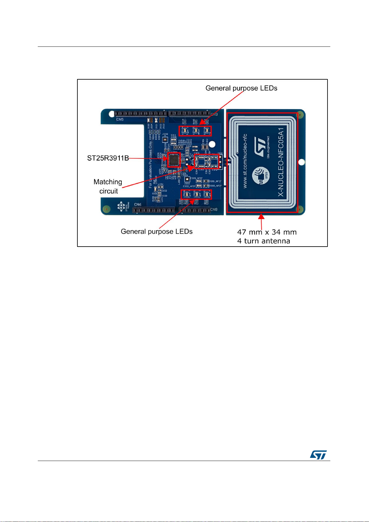
Figure 2: X-NUCLEO-NFC05A1 component placement
Page 11

UM2252
Component description
DocID030806 Rev 2
11/26
4 Component description
4.1 ST25R3911B device
The ST25R3911B-AQFT is a highly integrated NFC initiator/HF reader IC embedding:
the analog front end (AFE) and a highly integrated data framing system for:
ISO 18092 (NFCIP-1) initiator
ISO 18092 (NFCIP-1) active target
ISO 14443A and B reader (including high bit rates)
FeliCa™ reader
The implementation of other standard and custom protocols (like MIFARE™ Classic) is
possible by using the AFE and implementing framing in the external microcontroller
(Stream and Transparent modes).
4.2 Schematic diagrams
4.2.1 USB connectivity and power supply
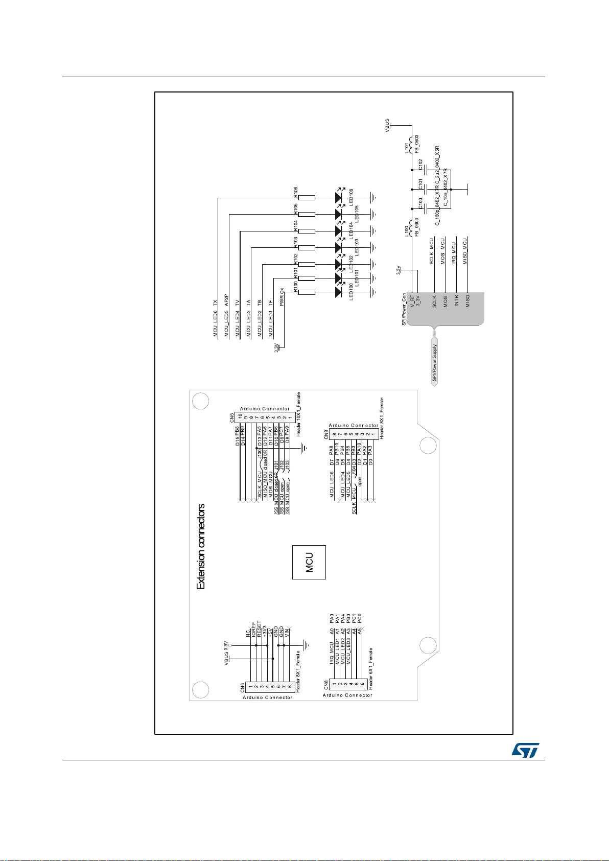
The X-NUCLEO-NFC05A1 expansion board can be connected via Arduino® UNO R3
connectors to the STM32 Nucleo board.
A green LED indicates if the 5 V supply is present on the X-NUCLEO-NFC05A1 expansion
board.
The six status LEDs are controlled via MCU.
Additional components are placed for the 5 V supply filtering.
Several solder jumpers enable an alternative connection of SCLK_MCU and /SS_MCU to
the STM32 MCU.
Page 12
Component description
UM2252
12/26
DocID030806 Rev 2
Figure 3: STM32 Nucleo connector schematic diagram
Page 13

UM2252
Component description
DocID030806 Rev 2
13/26
4.2.2 ST25R3911B schematic diagram
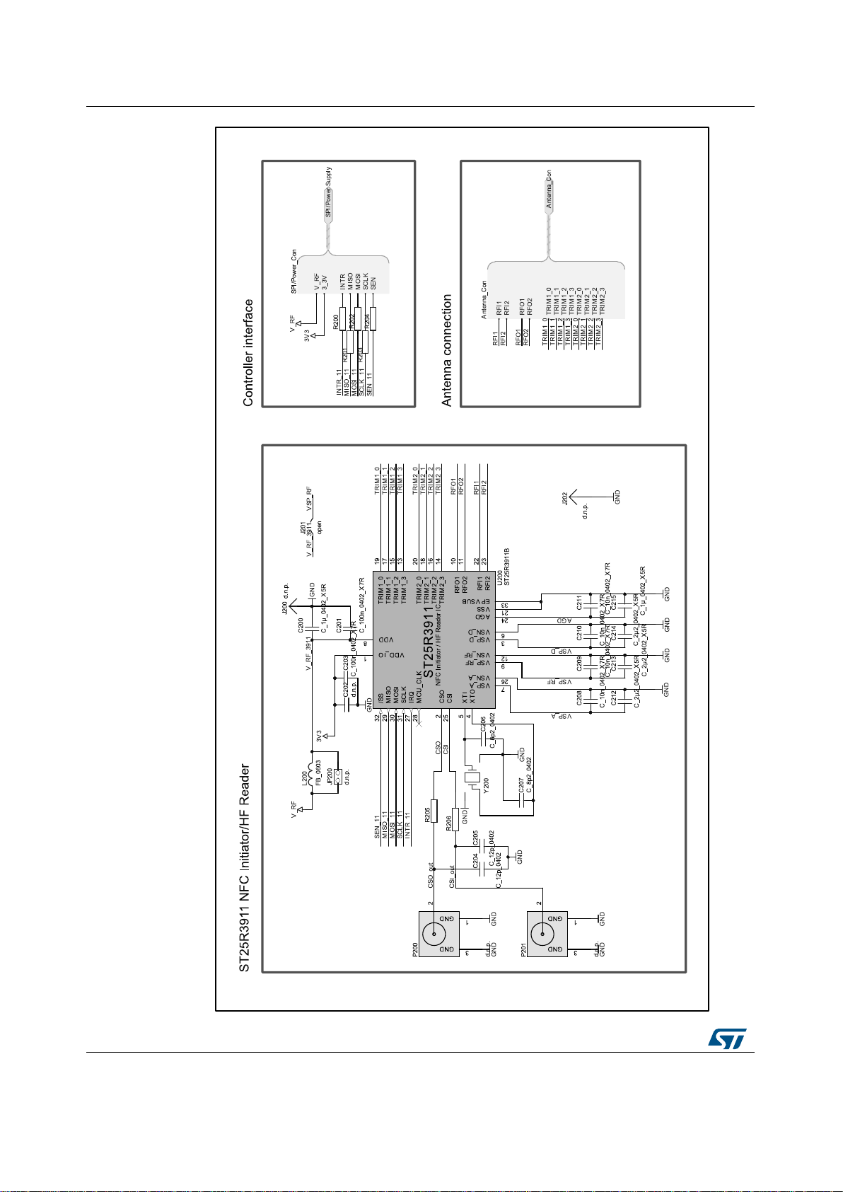
The ST25R3911B is directly connected to the filtered 5 V USB supply. There are additional
supply filtering components placed close to the NFC/HF reader IC.
Jumper JP200 can be used to measure the chip supply current.
If this measurement is performed, the ferrite beat L301 has to be removed.
Capacitors 200 to 203 provide additional filtering of the ST25R3911B supply.
During layout all decoupling capacitors have been placed as close as possible to the
ST25R3911B chip. Special care has been taken for C209, C201, C213 and C200 since
these decoupling capacitors are used for the high power driver stage.
To demonstrate the capacitive wake-up feature, two capacitive electrodes are placed on
the PCB. Additional electrodes can be connected using the P200 and P201 UFL
connectors.
For SPI cross-connecting another reader PCB, the resistors R200 to R204 can be
removed.
J201 allows to bypass the internal VSP_RF regulator in case the output current is > 200
mA and needs to be supported.
Page 14
Component description
UM2252
14/26
DocID030806 Rev 2
Figure 4: ST25R3911B schematic diagram
Page 15
UM2252
Component description
DocID030806 Rev 2
15/26
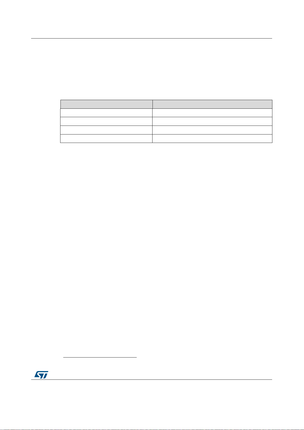
VHBR Matching
NFC Forum Matching
C302
C302_NFCF
C309
C309_NFCF
R300
R300_NFCF
R301
R301_NFCF
a
4.2.3 Antenna and matching network components
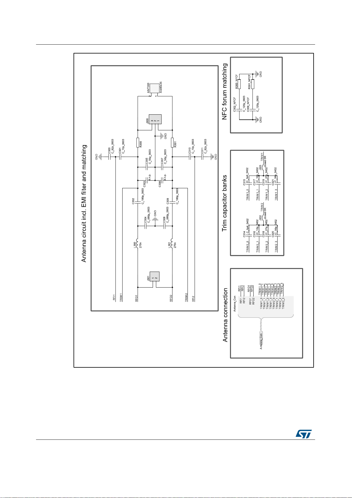
This schematic diagram contains the matching network and the automatic antenna tuning
capacitors as well as the alternative NFC Forum matching components.
In the default configuration, the X-NUCLEO-NFC05A1 expansion board is populated with a
VHBR tuning, which allows communication to speed up to 3.4 Mbps.
The Q-factor is doubled and bitrates up to 848kbps are supported, by switching the
components listed in the following table.
Table 3: Matching variant
To support VHBR bit rates, the antenna is matched to a system Q-Factor of 8.
By switching to the NFC Forum matching components, the system Q-Factor is increased to
16. This can increase read range by up to 20% depending on the communication
technology, but limits the maximum supported bit rate to 848kbps.a.
The etched PCB antenna can be easily removed from the expansion board to connect a
custom antenna using the connector J300.
The matching topology supports the connection of one custom differential antenna or two
single-ended antennas. The two single-ended antennas can then be multiplexed in
software using the single and rfo2 bits of IO Configuration Register 1.
Further information about antenna matching can be found at www.st.com/st25r
Page 16
Component description
UM2252
16/26
DocID030806 Rev 2
Figure 5: Matching circuit schematic diagram
Page 17
UM2252
Component description
DocID030806 Rev 2
17/26
4.3 PCB Layout
4.3.1 PCB layers
As the ST25R3911B is a high power RF transmitter, the NFC reader layout must be done
carefully.
The decoupling capacitors are located as close as possible to the positive and negative
power supply pins (for example VSP_RF and VSN_RF).
Since the chip is using a differential output driver stage, the antenna matching network is
treated as a differential network.
The space between the components is kept as small as possible and the whole network is
routed completely symmetrical.
Via stitching and via shielding is used to maintain a low impedance and prevent short
return current loops.
The RF traces are protected by via stitching in combination with guard rings to create a via
wall: this keeps the PCB electromagnetically 'quiet'.
A via shield is used to create a vertical copper barrier through the PCB, to help reduce
crosstalk and electromagnetic interference in a route carrying an RF signal.
The RFI traces and AAT lanes are routed as close as possible to each other.
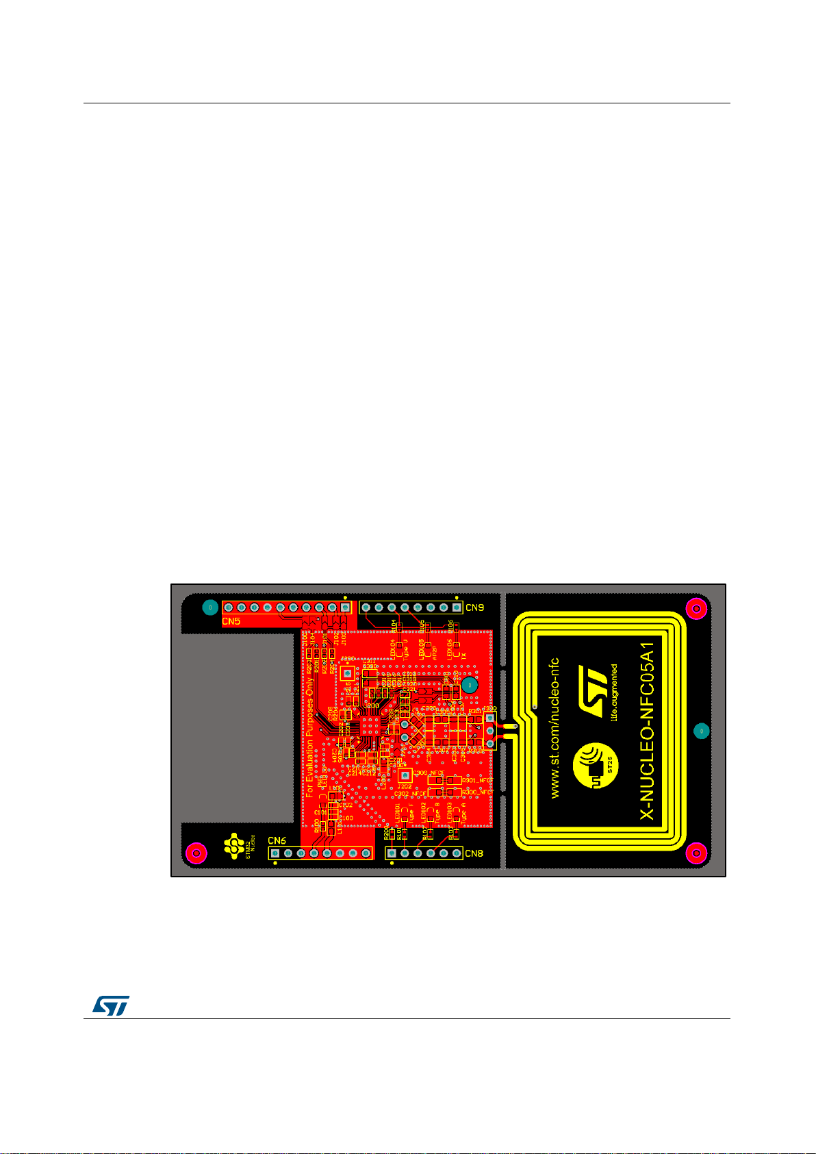
4.3.2 Top layer
The top layer contains most of the components and PCB traces. The unused areas around
the IC are filled with GND planes guarded using via stitching.
The important analog traces are surrounded by GND vias.
Figure 6: PCB layout top layer
Page 18
Component description
UM2252
18/26
DocID030806 Rev 2
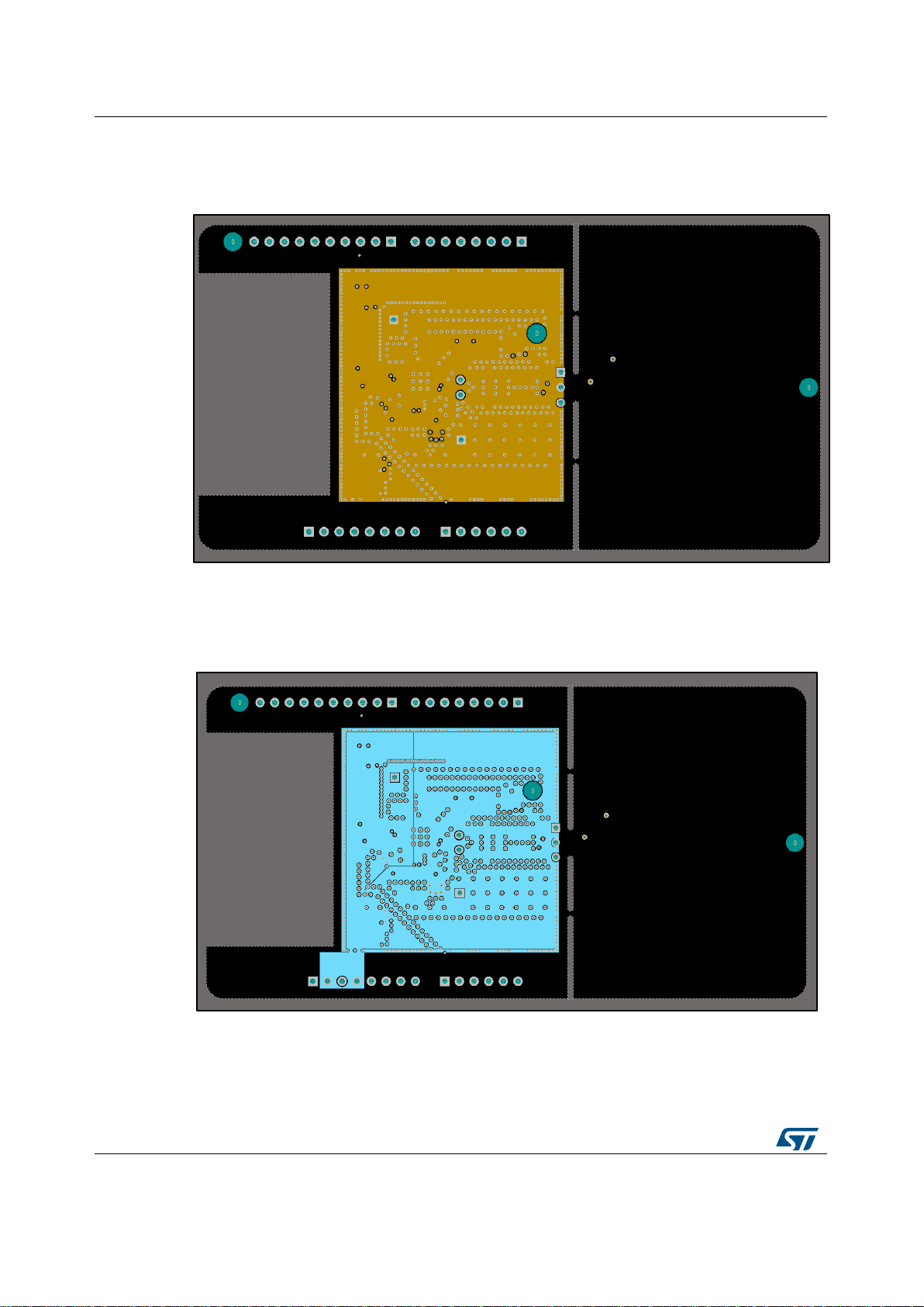
4.3.3 Mid layer 1
The mid layer 1 is a pure GND plane. It provides a low ohmic DC path for the GND
connection.
Figure 7: PCB layout mid layer 1
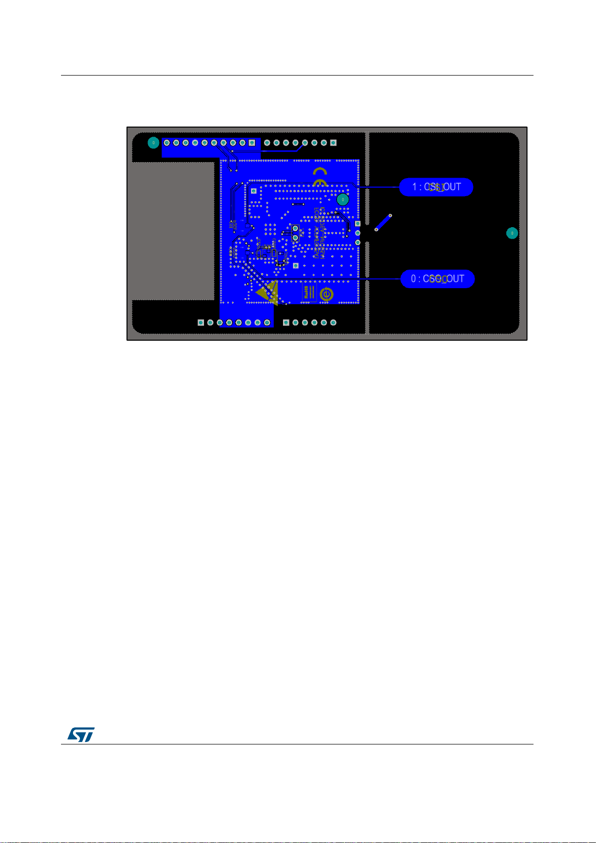
4.3.4 Mid layer 2
Mid layer 2 is used for power distribution. It contains the power planes for the ST25R3911B
5 V supply and the 3.3 V to communicate with the STM32 Nucleo board.
Figure 8: PCB layout mid layer 2
Page 19
UM2252
Component description
DocID030806 Rev 2
19/26
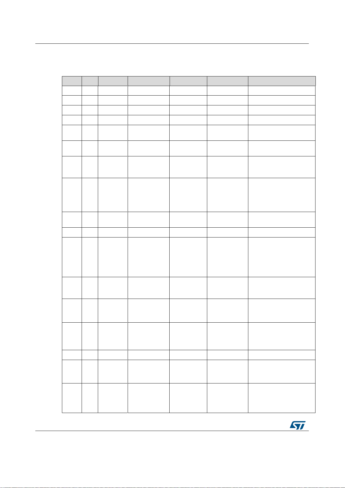
4.3.5 Bottom layer
The bottom layer is mainly GND plane. Some traces are routed through the bottom plane.
Figure 9: PCB layout bottom layer
Page 20
Bill of materials
UM2252
20/26
DocID030806 Rev 2
Item
Q.ty
Ref.
Part/Value
Description
Manufacturer
Order code
1 0 C202
DNM
2 0 J300
DNM
3 0 J301
DNM
4 0 JP200
DNM
5
0
C303,
C306
DNM
6
0
J200,
J202
DNM
7 1 C100
0402, 0.01 µF,
25 V, ± 10%,
X7R
AVX
0402YC101KAT2A
8
5
C101,
C208,
C209,
C210,
C211
0402, 0.01 µF,
25 V, ± 10%,
X7R
AVX
04023C103KAT2A
9
0
P200,
P201
DNM
HRS
(HIROSE)
U.FL-R-SMT-1(10)
10 1 LED100
Green LED
Lite-On
LTST-C190KGKT
11
6
LED101,
LED102,
LED103,
LED104,
LED105,
LED106
Blue LED
Lite-On
LTST-C190TBKT
12
2
C201,
C203
0402, 0.1 µF,
10 V, ± 10%,
X5R,
MULTICOMP
MC0402X104K100CT
13
2
C301,
C310
0603, 10 pF,
50 V, 1%, C0G
/ NP0
MULTICOMP
MC0603N100F500CT
14
4
J100,
J101,
J302,
J303
MULTICOMP
MC00625W040210R
15 1 Y200
Crystal
MURATA
XRCGB27M120F3M00R0
16
2
C200,
C215
0402, 1 µF,
16 V, ± 10%,
X5R,
MURATA
GRM155R61C105KA12D
17
2
C206,
C207
0402, 8.2 pF,
50 V, ±
0.25 pF, C0G /
NP0
MURATA
GRM1555C1H8R2CA01D
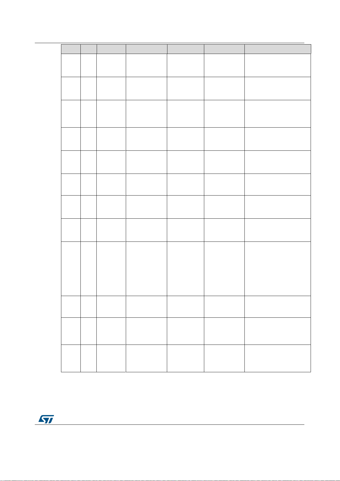
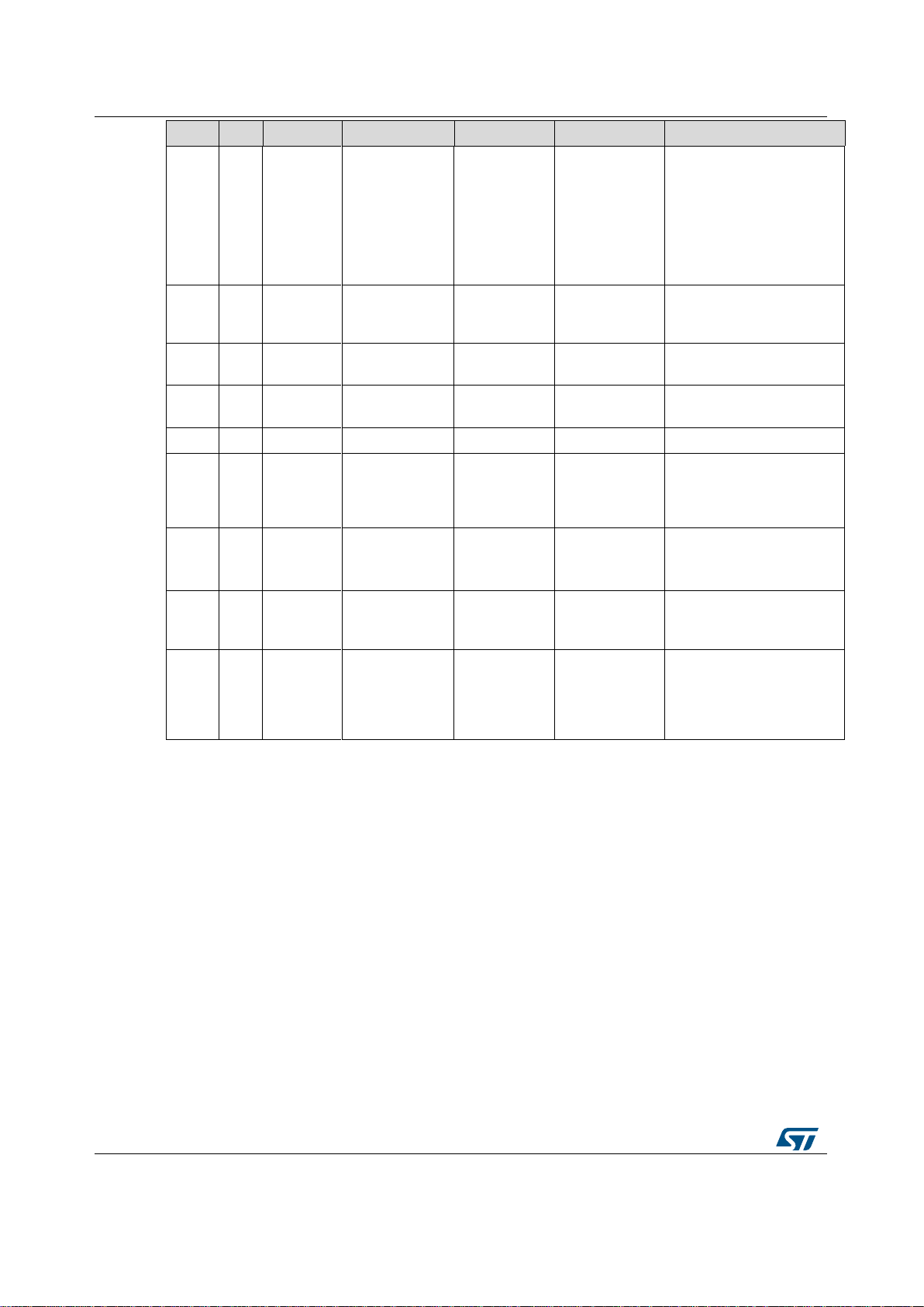
5 Bill of materials
Table 4: X-NUCLEO-NFC05A1 bill of materials
Page 21
UM2252
Bill of materials
DocID030806 Rev 2
21/26
Item
Q.ty
Ref.
Part/Value
Description
Manufacturer
Order code
18
2
C300,
C311
82 pF ±1%
50 V C0G,
NP0 0603
MURATA
GRM1885C1H820FA01D
19
2
C302,
C309
180 pF ±2%
50 V C0G,
NP0 0603
MURATA
GRM1885C1H181GA01D
20
2
C302_NF
CF,
C309_NF
CF
120 pF ±2%
50 V C0G,
NP0 0603
MURATA
GRM1885C1H121GA01D
21
2
C304,
C308
680 pF ±2%
50 V C0G,
NP0 0603
MURATA
GRM1885C1H681GA01D
22
2
C305,
C307
56 pF ±2%
50 V C0G,
NP0 0603
MURATA
GRM1885C1H560FA01D
23
2
C314,
C315
5.6 pF ±0.5 pF
50 V C0G,
NP0 0402
MURATA
GRM1555C1H5R6DA01D
24
2
C318,
C319
27 pF ±2%
50 V C0G,
NP0 0402
MURATA
GRM1555C1H270GA01D
25
2
C320,
C321
56 pF ±2%
50 V C0G,
NP0 0402
MURATA
GRM1555C1H560GA01D
26
2
L300,
L301
Unshielded
Wirewound
Inductor
MURATA
LQW18ANR27G80D
27
3
L100,
L101,
L200
MURATA
BLM18EG471SN1D
28
4
C102,
C212,
C213,
C214
0402, 2.2 µF,
6.3 V, ± 20%,
X5R
MURATA
GRM155R60J225ME15D
29
4
C204,
C205,
C316,
C317
12 pF ±2%
50 V C0G,
NP0 0402
MURATA
GRM1555C1H120GA01D
Page 22
Bill of materials
UM2252
22/26
DocID030806 Rev 2
Item
Q.ty
Ref.
Part/Value
Description
Manufacturer
Order code
30
8
R101,
R102,
R103,
R104,
R105,
R106,
R205,
R206
1 kohm, 50 V,
0402,
>100 mW,
± 5%
Panasonic
ERJ2GEJ102X
31 1 CN5
Header
10X1_Femal
e
Samtec
SSQ-110-03-L-S
32 1 CN8
Header
6X1_Female
Samtec
SSQ-106-03-L-S
33
2
CN6,
CN9
Header
8X1_Female
Samtec
SSQ-108-03-L-S
34 1 U200
ST
ST25R3911B-AQFT
35
2
R300_NF
CF,
R301_NF
CF
1.96 Ohm ±1%
0.1 W, 1/10 W
0603
Chip Resistor
Vishay Dale
CRCW06031R96FKEA
36 1 R100
680 Ohm ±5%
0.063 W,
1/16 W 0402
Chip Resistor
Yageo
RC0402JR-07680RL
37
2
R300,
R301
5.6 Ohm ±5%
0.1 W, 1/10 W
0603
Chip Resistor
Yageo
RC0603FR-075R62L
38
5
R200,
R201,
R202,
R203,
R204
220 Ohm ±5%
0.063 W,
1/16 W 0402
Chip Resistor
Yageo
RC0402JR-07220RL
Page 23

UM2252
Federal Communications Commission (FCC) and
Industry Canada (IC) compliance
DocID030806 Rev 2
23/26
6 Federal Communications Commission (FCC) and
Industry Canada (IC) compliance
6.1 FCC Compliance Statement
6.1.1 Part 15.19
This device complies with Part 15 of the FCC Rules. Operation is subject to the following
two conditions: (1) this device may not cause harmful interference, and (2) this device must
accept any interference received, including interference that may cause undesired
operation.
6.1.2 Part 15.21
Any changes or modifications to this equipment not expressly approved by
STMicroelectronics may cause harmful interference and void the user’s authority to operate
this equipment.
6.1.3 Part 15.105
This equipment has been tested and found to comply with the limits for a Class B digital
device, pursuant to part 15 of the FCC Rules. These limits are designed to provide
reasonable protection against harmful interference in a residential installation. This
equipment generates, uses and can radiate radio frequency energy and, if not installed and
used in accordance with the instructions, may cause harmful interference to radio
communications. However, there is no guarantee that interference will not occur in a
particular installation. If this equipment does cause harmful interference to radio or
television reception, which can be determined by turning the equipment off and on, the user
is encouraged to try to correct the interference by one or more of the following measures:
— Reorient or relocate the receiving antenna.
— Increase the separation between the equipment and receiver.
— Connect the equipment into an outlet on a circuit different from that to which the
receiver is connected.
— Consult the dealer or an experienced radio/TV technician for help.
6.1.4 FCC ID
FCC ID: YCPNFC05A1
6.2 Formal notices required by Industry Canada (“IC”)
6.2.1 Compliance Statement
This device complies with Industry Canada licence-exempt RSS standard(s). Operation is
subject to the following two conditions: (1) this device may not cause interference, and (2)
this device must accept any interference, including interference that may cause undesired
operation.
6.2.2 Declaration de Conformité
Le présent appareil est conforme aux CNR d’Industrie Canada applicables aux appareils
radio exempts de licence. L’exploitation est autorisée aux deux conditions suivantes: (1)
l’appareil ne doit pas produire de brouillage, et (2) l’utilisateur de l’appareil doit accepter
Page 24

Federal Communications Commission (FCC) and
Industry Canada (IC) compliance
UM2252
24/26
DocID030806 Rev 2
tout brouillage radioélectrique subi, même si le brouillage est susceptible d’en
compromettre le fonctionnement.
6.2.3 IC ID
IC ID: 8976A-NFC05A1
Page 25
UM2252
Revision history
DocID030806 Rev 2
25/26
Date
Version
Changes
06-Jul-2017
1
Initial release
31-Jul-2017
2
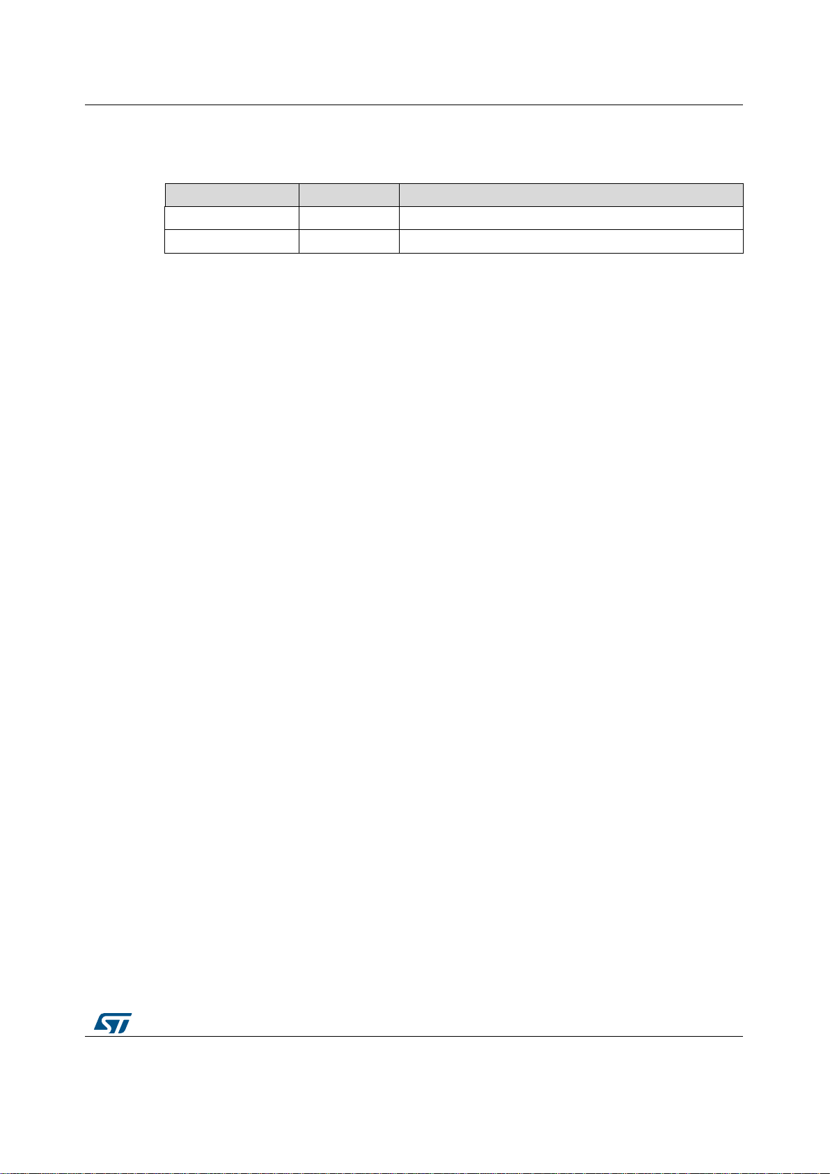
Added Section 6.1.3: "Part 15.105"
7 Revision history
Table 5: Document revision history
Page 26

UM2252
26/26
DocID030806 Rev 2
IMPORTANT NOTICE – PLEASE READ CAREFULLY
STMicroelectronics NV and its subsidiaries (“ST”) reserve the right to make changes, corrections, enhancements, modifications , and
improvements to ST products and/or to this document at any time without notice. Purchasers should obtain the latest relevant information on ST
products before placing orders. ST products are sold pursuant to ST’s terms and conditions of sale in place at the time of order
acknowledgement.
Purchasers are solely responsible for the choice, selection, and use of ST products and ST assumes no liability for application assistance or the
design of Purchasers’ products.
No license, express or implied, to any intellectual property right is granted by ST herein.
Resale of ST products with provisions different from the information set forth herein shall void any warranty granted by ST for such product.
ST and the ST logo are trademarks of ST. All other product or service names are the property of their respective owners.
Information in this document supersedes and replaces information previously supplied in any prior versions of this document.
© 2017 STMicroelectronics – All rights reserved
 Loading...