

Page 1

UM3020
User manual
Getting started with the X-NUCLEO-GNSS2A1 expansion board based on the
eseo-VIC3DA dead-reckoning GNSS module for STM32 Nucleo
T
Introduction
The X-NUCLEO-GNSS2A1 expansion board is based on the T
easy-to-use, global navigation satellite system (GNSS) module, which embeds a TeseoIII single die standalone positioning
receiver IC, usable in different configurations in your STM32 Nucleo project.
The Teseo-VIC3DA is a compact (16.0 x 12.2 mm) module that provides superior accuracy thanks to the on-board temperature
compensated crystal oscillator (TCXO) and a reduced time-to-first fix (TTFF) with its dedicated real-time clock (RTC) oscillator.
The Teseo-VIC3DA module runs the GNSS firmware (X-CUBE-GNSS1) to perform all the GNSS operations including
acquisition, tracking, navigation, and data output without any external memory support.
The X-NUCLEO-GNSS2A1 expansion board is compatible with the Arduino UNO R3 connector and the ST morpho connector. It
can be plugged to an STM32 Nucleo development board and stacked with additional STM32 Nucleo expansion boards.
Figure 1. X-NUCLEO-GNSS2A1 expansion board
eseo-VIC3DA tiny GNSS module. It represents an affordable,
UM3020 - Rev 1 - July 2022
For further information contact your local STMicroelectronics sales of
fice.
www.st.com
Page 2

1 Getting started
1.1 Board overview
The X-NUCLEO-GNSS2A1
reckoning that covers a wide range of applications where geo-location is required.
The key features are:
• Operating supply voltage: 3.3 V
• Ambient temperature: -40/+85°C
• Sensitivity: -163 dBm (tracking mode)
• Interfaces:
– a UART port
– an I²C port
– configurable digital I/O time pulse
– EXTINT input for wake-up
• NMEA protocol
• Assisted GNSS:
– autonomous AGNSS
– real-time, server-based
• Simultaneous multiconstellation:
– GPS
– Galileo
– Glonass
– BeiDou
– QZSS
• Compatible with STM32 Nucleo development boards
• Compatible with the Arduino UNO R3 connector
• Teseo-VIC3DA dead-reckoning automotive firmware
• Provision of FWD and WHEELTICK signals
• Automotive GNSS and 6-axis inertial sensor
• LNA and SAW filters on the RF path
• SMA female antenna connector
• RoHS and WEEE compliant
UM3020
Getting started
expansion board for STM32 Nucleo is a GNSS multiconstellation receiver with dead-
UM3020 - Rev 1
page 2/21
Page 3

1.2 Hardware and software requirements
The X-NUCLEO-GNSS2A1 must be plugged onto an STM32 Nucleo development board through the Arduino
UNO R3 connectors, as shown in the figure below
Figure 2. X-NUCLEO-GNSS2A1 expansion board connected to an STM32 Nucleo development board
.
UM3020
Hardware and software requirements
UM3020 - Rev 1
The X-NUCLEO-GNSS2A1 can be connected to any STM32 Nucleo development board, even though complete
testing has been performed on the NUCLEO-F401RE board.
T
o use the STM32 Nucleo development boards with the X-NUCLEO-GNSS2A1 expansion board, the following
software and hardware specifications are required:
• a PC with Microsoft Windows® 10 to install the software package (X-CUBE-GNSS1);
• an STM32 Nucleo development board (NUCLEO-L053R8 or NUCLEO-F401RE);
• a type A to mini-B USB cable to connect the STM32 Nucleo to the PC;
• the X-CUBE-GNSS1 software package;
• TESEO-SUITE.
The installation of the X-CUBE-GNSS1 and the TESEO-SUITE graphical user interface utility on the user PC
requires:
• 128 MB of RAM;
• 40 MB of hard disk space.
page 3/21
Page 4

1.3 Board setup
UM3020
Board setup
To set up the X-NUCLEO-GNSS2A1 expansion board, follow the procedure below
.
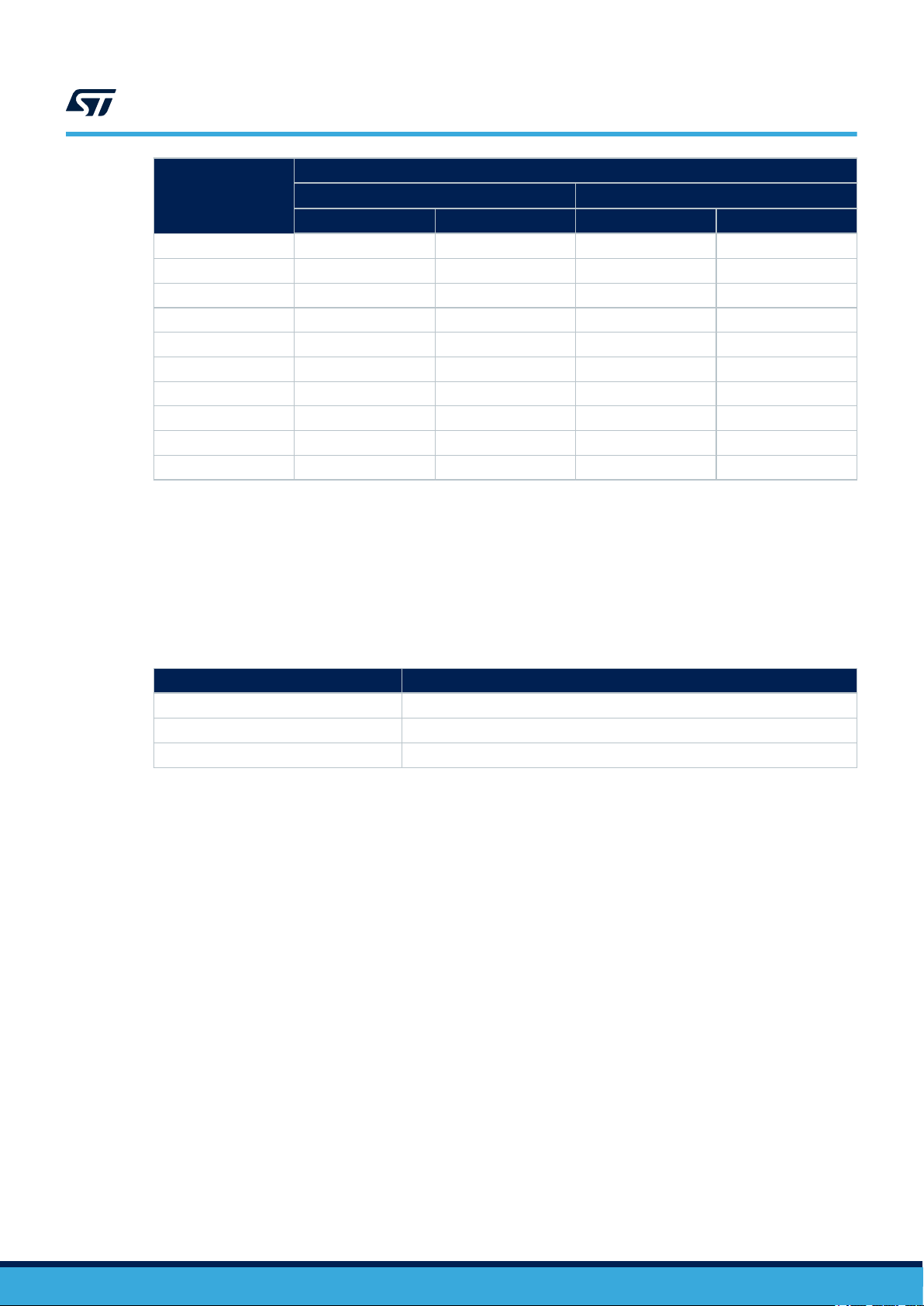
Step 1. Check the jumper position shown below:
Table 1. X-NUCLEO-GNSS2A1 expansion board - jumper 1 default settings
Signal Jumper Configuration
I²C-SCL J11 Closed
I²C-SDA J12 Closed
VCC-VCC_IO J14 Closed
V14Bat J15 Closed
SYS_FWD J23 1-2
SYS_WHEELTICK J24 2-3
SYS_RESETn J25 1-2
SYS_WAKEUP J26 2-3
UART-RX J27 2-3
UART-TX J28 2-3
SYS_PPS J29 1-2
SYS_IRQ J30 2-3
Step 2. Connect the X-NUCLEO-GNSS2A1 to the STM32 Nucleo development board.
Step 3. Power the STM32 Nucleo
development board using the type A mini-B USB cable.
Step 4. Program the STM32 Nucleo development board using the firmware example provided.
Step 5. Reset the MCU via the STM32 Nucleo development board [reset] button.
The evaluation kit is ready-to-use.
UM3020 - Rev 1
page 4/21
Page 5

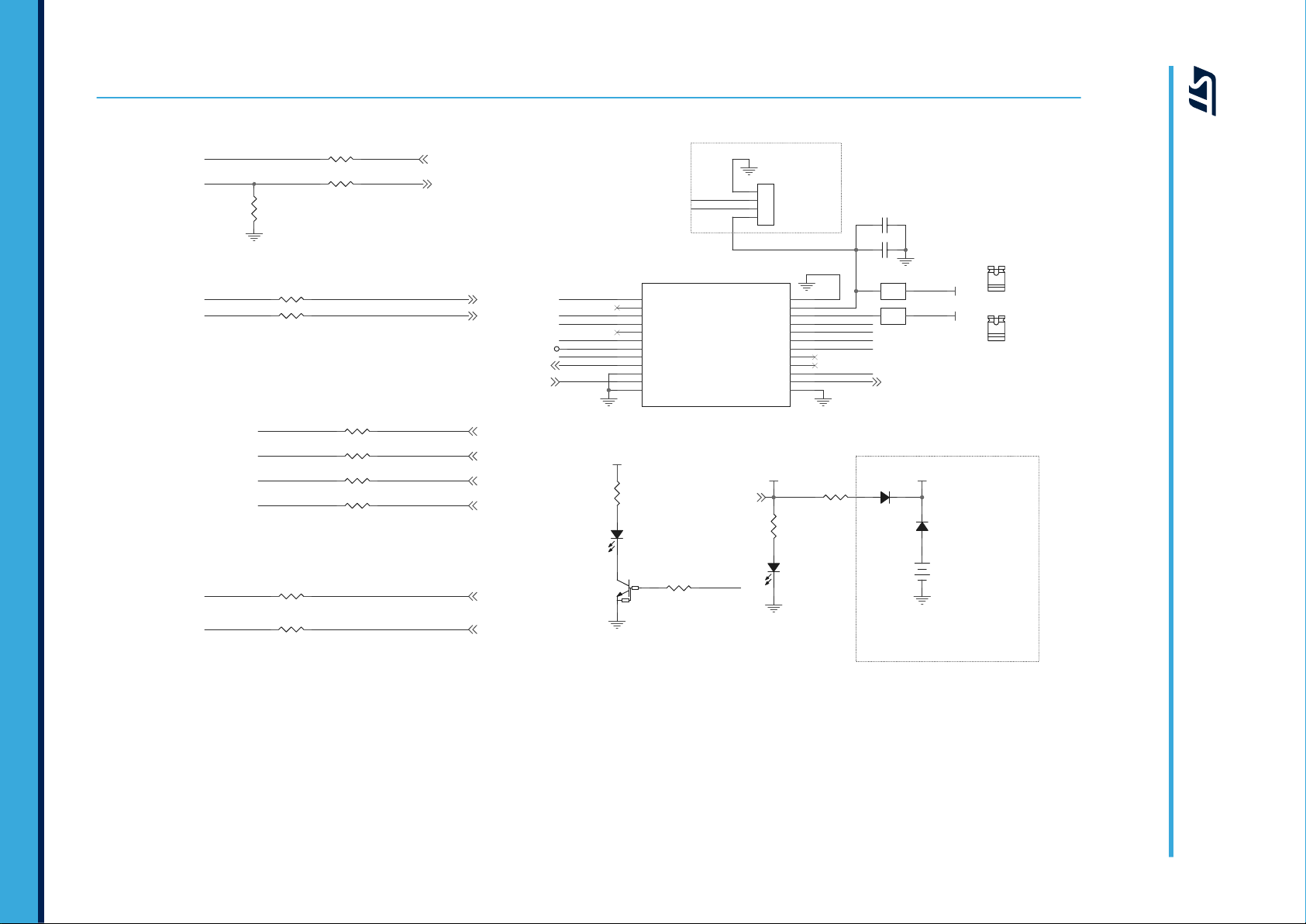
2 Hardware description
2.1 X-NUCLEO-GNSS2A1 expansion board for STM32 Nucleo
The X-NUCLEO-GNSS2A1 allows testing the T
package contained in the X-CUBE-GNSS1 software.
Important: Program the microcontroller on the STM32 Nucleo development board.
The Teseo-VIC3DA module and the STM32 Nucleo development board communicate through the expansion
board connectors (CN5, CN6, CN8, and CN9) as listed in the tables below.
Table 2. Interconnection between STM32 Nucleo development board and X-NUCLEO-GNSS2A1 expansion
STM32 Nucleo pins
NC
IOREF 2 3V3
RESET 3
3V3 4 3V3
5V 5
GND 6 GND
GND 7 GND
VIN 8
A0 1
A1 2
A2 3
A3 4
A4 5
A5 6
eseo-VIC3DA GNSS module functionality via the firmware
board (left-side connectors)
X-NUCLEO-GNSS2A1
CN6 (power)
Pin Signal
X
UM3020
Hardware description
CN8 (analog)
UM3020 - Rev 1
Table 3. Interconnection between STM32 Nucleo development board and X-NUCLEO-GNSS2A1 expansion
board (right-side connectors)
X-NUCLEO-GNSS2A1
STM32 Nucleo pins
D15
D14 9 SDA2
AREF 8
GND 7 GND
D13 6 WAKE_UP
D12 5
D11 4
D10 3
CN5 (digital) CN9 (digital)
Pin Signal Pin Signal
10 SCL2
page 5/21
Page 6
STM32 Nucleo pins
D9
D8 1 RX0
D7 8 RESET
D6 7 PPS
D5 6
D4 5 WAKE_UP
D3 4
D2 3 TX0/PPS
D1 2 RX
D0 1 TX
2.2 Teseo-VIC3DA module
The X-NUCLEO-GNSS2A1 expansion board embeds the T
module with 6-axis IMU.
The Teseo-VIC3DA is an easy-to-use global navigation satellite system (GNSS) standalone module. It embeds
the TeseoIII single-die standalone positioning receiver IC, which works simultaneously on multiple constellations
(GPS/Galileo/Glonass/BeiDou/QZSS).
UM3020
Teseo-VIC3DA module
X-NUCLEO-GNSS2A1
CN5 (digital) CN9 (digital)
Pin Signal Pin Signal
2 RESET
eseo-VIC3DA automotive GNSS dead-reckoning
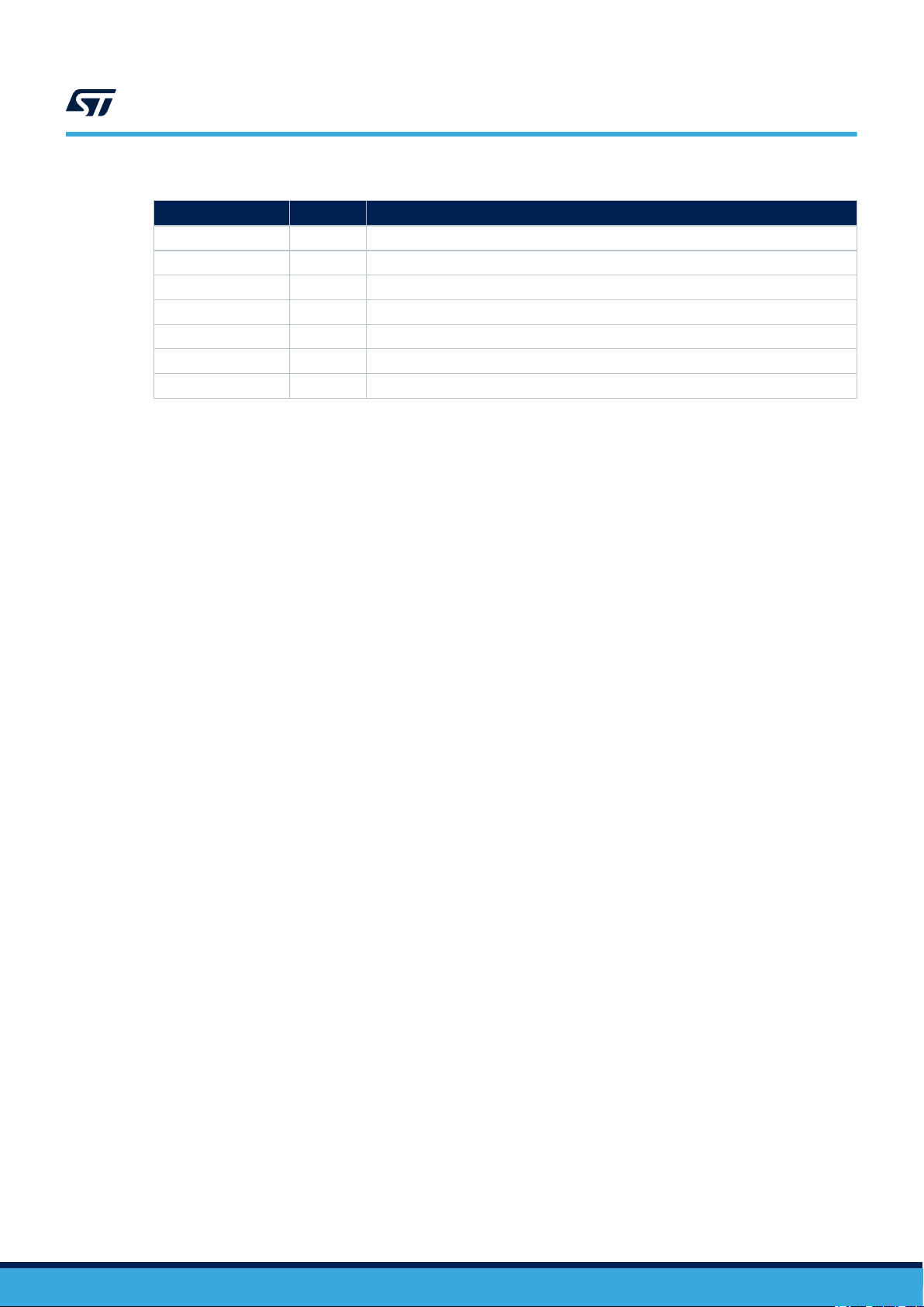
Table 4. Teseo-VIC3DA details
Feature Description
Sales type Teseo-VIC3DA
Package LLC 24 pins (16.0 mm x 12.2 mm)
Operating voltage 3.3 V
2.3 GNSS antenna
The GNSS antenna (manufacturer INPAQ, part number B3G02G-S3-XX-A) is attached to the board through a
SMA connector (with its trademark and model).
Important:
The antenna provided by the manufacturer can be replaced only with an identical one.
2.4 UART, I²C, and GPIO connection options
The T
eseo-VIC3DA module embedded in the X-NUCLEO-GNSS2A1 expansion board can be used to work with
the board in different configurations when different expansion boards are used and a conflict of signals occurs.
UM3020 - Rev 1
page 6/21
Page 7
UM3020
Current measurement
Table 5. X-NUCLEO-GNSS2A1 expansion board: T
Signal Pins STM32 Nucleo (optional connections)
I²C-SCL d15 -
I²C-SDA d14 -
Wakeup d13 d4
Reset d7 d9
PPS d6 d2
UART-RX d8 d1
UART-TX d2 d0
For the optional connections, modify the firmware according to the STM32 resources to be used.
2.5 Current measurement
To monitor the T
J15 pin (VBAT).
As the Teseo-VIC3DA power consumption is very low during most of its operating time, an accurate instrument in
the range of few μA is required.
eseo-VIC3DA module power consumption, insert an ammeter probe between J14 pin (VCC) and
2.6 ODO connector
The ODO connector on the X-NUCLEO-GNSS2A1 exposes two input signals for the T
embeds the TESEO dead reckoning. These two signals are specific to dead-reckoning applications and provide
the odometer information using the pins FWD (pin2) and WHEELTICK (pin3).
eseo-VIC3DA interface with the STM32 Nucleo
development board
eseo-VIC3DA, which
UM3020 - Rev 1
page 7/21
Page 8

X-NUCLEO-GNSS2A1 expansion board component placement
2.7 X-NUCLEO-GNSS2A1 expansion board component placement
Figure 3. X-NUCLEO-GNSS2A1 expansion board component placement details
UM3020
UM3020 - Rev 1
page 8/21
Page 9
GNSS Module
Battery
SMD0402
SMD0603
SMD0603
SMD0603
SMD0603
SMD0603
SMD0603
SMD0603
ODO Connector
SMD0402
+VCC_IO
Battery Holder (CR2032)
+VCC_IO +VBatt
GND
GND
GND
GND
+VBatt
GND
+VCC_IO
GND
GND
GND
GND
+VCC_IO
SYS_RESETn
TX
SYS_WAKEUP
RX
I2C_CLOCK
I2C_DATA
AntOFFRF_IN
VCC_RF
SYS_FWD
SYS_WHEELTICK
SYS_IRQ
SYS_PPS
C14100pF
R10
330E
D3
Green_LED
J16
1
2
3
4
con4-strip-male
D5
BAT20J
R38 0E
J14
HEADER1x2
1
1
Closed
2
2
R8
330E
R11
0E
R420E
D2
Red_LED
R2
R1
Q1
1
2
MUN2214T1G
3
R44 0E
R41 0E
R37 0E
R33
NM
R40 0E
R390E
C13100nF
R36 0E
JR14
R35 0E
SHUNT 2.54 mm.
JR15
TP1
R43SHUNT 2.54 mm.0E
J15
HEADER1x2
1
1
Closed
2
2
D1
BAT20J
U1
1
TESEO-VIC3DATR
WakeUp
2
Reserved
PPS
3
4
WHEELTICK
5
IRQ
6
Reserved_1
7
Reserved_2
8
nReset
9
VCC_RF
GND
10
11
RF_IN
GND
12
GND
13
14
AntOFF
FWD
15
16
Reserved_3
17
Reserved_4
18
I2C_SDA
19
I2C_SCL
20
UART-TX
21
UART-RX
22
V_BAT
VCC
23
GND
24
VL1
NM
R9
0E
PPS
RESETn
SYS_RESETn
SYS_WAKEUP
WAKEUP
RX
UART_TX
TX
I2C_SDA
I2C_SCL
I2C_DATA
I2C_CLOCK
UART_RX
UART_TX
UART_RX
I2C_SCL
I2C_SDA
WAKEUP
PPS
AntOFF
RF_IN
RESETn
VCC_RF
FWD
WHEELTICK
FWD
WHEELTICK
IRQ
FWD
SYS_FWD
WHEELTICK
IRQ
SYS_WHEELTICK
SYS_IRQ
PPS
SYS_PPS
UM3020 - Rev 1
3 Schematic diagrams
Figure 4. X-NUCLEO-GNSS2A1 circuit schematic (1 of 3)
page 9/21
Schematic diagrams
UM3020
Page 10

NUCLEO CONNECTORS
CN7 of NUCLEO BOARD
CN8 of NUCLEO BOARDCN6 of NUCLEO BOARD
CN10 of NUCLEO BOARD
CN5 of NUCLEO BOARDCN9 of NUCLEO BOARD
{Default}
{Default}
{D8 = PA9: STM32 USART1_TX}
{Default}
{Default}
{Default}
{Default}
{Default}
{Default}
+3V3
+3V3
IOREF
GND
RX
I2C_CLOCK
I2C_DATA
+VCC_IO
SYS_FWD
SYS_WHEELTICK
SYS_RESETn
TX
SYS_WAKEUP SYS_PPS
SYS_IRQ
J28
1
2
HEADER1X3
3
JR17
NM
CN10
1
ST morpho
2
3 4
5 6
7 8
9 10
11 12
1314
15 16
17 18
19 20
21 22
23 24
25 26
2728
29 30
31 32
3334
35 36
3738
CN6
1
Arduino
2
3
4
5
6
7
8
J11
1
HEADER1x2
1
Closed
2
2
J24
1
2
HEADER1X3
3
CN5
1
Arduino
2
3
4
5
6
7
8
9
10
CN8
1
Arduino
2
3
4
5
6
JR9
J26
SHUNT 2.54 mm.
1
2
HEADER1X3
3
CN9
1
Arduino
2
3
4
5
6
7
8
J23
1
2
HEADER1X3
3
J12
HEADER1x2
1
1
Closed
2
2
JR13
NM
CN7
1 2
ST morpho
3 4
5 6
7 8
9 10
11 12
13 14
1516
17 18
1920
21 22
23 24
25 26
27 28
29 30
31 32
3334
35 36
37 38
J25
1
2
HEADER1X3
3
JR11
SHUNT 2.54 mm.
JR12
SHUNT 2.54 mm.
JR19
SHUNT 2.54 mm.
JR18
J29
SHUNT 2.54 mm.
1
2
HEADER1X3
3
J30
1
2
HEADER1X3
3
JR2
J27
SHUNT 2.54 mm.
1
2
HEADER1X3
3
JR16
SHUNT 2.54 mm.
JR4
PC11
PD2
SHUNT 2.54 mm.
E5V
GND
IOREF
RESET
+3V3
+5V
GND
GND
VIN
PA0A0
PA1 A1
PA4 A2
PB0A3
PC1 A4
PC0 A5
D7 PA8
D5/PWMPB4
D6/PWMPB10
D4 PB5
PB3D3/PWM
D2 PA10
D1/RX PA2
D0/TXPA3
PC10
PC12
VDD
BOOT0
NC/PF6
NC/PF7
PA13
PA14
PA15
GND
PB7
PC13
PC14
PC15
PH0/PF0/PD0
PH1/PF1/PD1
PC2
VLCD/VBAT
PC3
PC8
PC6
PC5
U5V
PD8
PA12
PA11
PB12
PB11/NC
GND
PB2
PB1
PB15
PB14
PB13
AGND
PC4
NC/PF5
NC/PF4
PB8D15/SCL
PB9D14/SDA
AVDD
GND
PA5D13/SCK
PA6D12/MISO
PA7D11/MOSI/PWM
PB6D10/CS/PWM
PC7D9/PWM
D8 PA9
PC9
D15/SCL
D14/SDA
RX
D6/PWM
D7 D8
SHUNT 2.54 mm.
{Default}
D4
D9/PWM
D4
SHUNT 2.54 mm.
{Default}
D7
D13/SCK
D8
SYS_WAKEUP
D1/RX
D0/TX D2
D2D6/PWM
SYS_PPS
{D2 = PA10: STM32 USART1_RX}
TX
D13/SCK D9/PWM
SYS_IRQ
UM3020 - Rev 1
Figure 5. X-NUCLEO-GNSS2A1 circuit schematic (2 of 3)
page 10/21
Schematic diagrams
UM3020
Page 11

RF In Section
SMD0402
SMD0402
SMD0402
SMD0402
SMD0402
SMD0402
SMD0603
SMD0402
SMD0402
SMD0402
SMD0402
SMD0402
SMD0402
SMD0402
SMD0402
SMD0402
SMD0805
SMD0805
SMD0402
NM
SMD0402
SMD0402
SMD0402
GND
GND
GND
GND
GND
GND
GND
GND
GND
GND
RF_IN
VCC_RF
AntOFF
R46
0E C2
120pF
L1
6.8nH
CN1
SMA
U2
1
BGA824N6
GND
VCC
2
A0
3
AI
5
4
GND-RF
PON
6
R260E
R20
0E
C9
56pF
R15
0E
C3
120pF
R22
NM
R18
NM
R21
100k
C1
1nF
R230E
U3
TPS22943
1
Vout
GND
2
OC
3
5
Vin
ON
4
D4
R25NM
ESDARF02-1BU2CK
R45
NM
C5
3.9pF
C8
2.2uF
L2
56nH
C7
1uF
R270E
R24
10k
1
R17
NM
J31Taoglas CGGBP.18.4.A.02
Z1
1
B4327
2
543
VCC_RF
UM3020 - Rev 1
Figure 6. X-NUCLEO-GNSS2A1 circuit schematic (3 of 3)
page 11/21
Schematic diagrams
UM3020
Page 12
4 Bill of materials
Item Q.ty Ref. Value Description Manufacturer Order code
1 1 CN1
UM3020
Bill of materials
Table 6. X-NUCLEO-GNSS2A1 bill of materials
SMA,
COAX_SMA_EDGESMA jack Molex 73251-1150
2 1 CN5
3 2 CN6, CN9
4 0 CN7,CN10
5 1 CN8
6 1 C1
7 2 C2,C3
8 1 C5
9 1 C7
10 1 C8
11 1 C9
12 1 C13
13 1 C14
14 2 D1, D5
15 1 D2
16 1 D3
17 1 D4
JR2, JR4,
JR9, JR1
JR12,
JR13,
18 12
JR14,
JR15,
JR16,
JR17,
JR18,
JR19
ARDUINO_10x1,
TH
ARDUINO_8x1,
TH
ST_MORPHO_19
x2, TH
ARDUINO_6x1,
TH
1 nF, SMD 0402,
16 V
, X7R
120 pF, SMD
0402, 16 V
3.9 pF, SMD
0402, 16 V
1 µF, SMD 0805,
16 V
, X7R
2.2 µF, SMD0805,
16 V
, X7R
56 pF, SMD 0402,
16 V
, X7R
100 nF, SMD
0402, 16 V
100 pF, SMD
0402, 16 V
BAT20JFILM,
SOD323
Red_LED, SMD
0603
Green_LED, SMD
0603
ESDARF02-1BU2
CK, ST0201
1,
2.54 mm, TH, 3 A
max.
, NP0
, NP0
, X7R
, COG
Elevated socket 4UCONN 15286
Elevated sockets 4UCONN 15284
Elevated sockets
(not mounted)
Elevated socket 4UCONN 15282
Chip capacitor Murata
Chip capacitors Murata
Chip capacitor Murata
Chip capacitor Taiyo Yuden EMK212B7105KGHT
Chip capacitor Taiyo Yuden EMK212B7225KGHT
Chip capacitor Murata
Chip capacitor Murata
Chip capacitor Murata
23 V, 1 A general
purpose signal
Schottky diodes
Diode LED Lite-On LTST-C193KRKT-5A
Diode LED Lite-On LTST-C191KGKT
Single line
bidirectional
ESD protection
for high-speed
interfaces
Jumpers
4UCONN 8413
GRM155R71H102KA01
D
GRM1555C1H121JA01
D
GRM1555C1H3R9WA01
D
GRM1555C1H560JA01
D
GRM155R71C104KA88
D
GRM1555C1H101JA01
D
ST BAT20JFILM
ST ESDARF02-1BU2CK
TE
Connectivity/AMP
1-382811-6
UM3020 - Rev 1
page 12/21
Page 13
Bill of materials
Item Q.ty Ref. Value Description Manufacturer Order code
19 4
20 1 J16
21 8
22 1 J31
23 1 L1
J11, J12,
J14, J15
J23, J24,
J25, J26,
J27, J28,
J29, J30
HEADER1x2, TH,
2.54 mm, 2-pin,
single row
HEADER1x4, TH,
2.54 mm, 4-pin,
single row
HEADER1x3, TH,
2.54 mm, 3-pin,
single row
Taoglas
CGGBP
.18.4.A.02
, 18 mm x 18 mm
x 4 mm (pin
mount)
6.8 nH, SMD
0402, 0.7 A, ±0.02%SMD inductor Murata LQW15AN6N8G00D
Headers Wurth Elektronik 61300211121
Header Wurth Elektronik 61300411121
Headers Wurth Elektronik 61300311121
RF antenna (not
mounted)
Taoglas CGGBP.18.4.A.02
UM3020
24 1 L2
25 1 Q1
26 2 R8, R10
R9, R11,
R35, R36,
27 12
28 6
29 1 R21
30 1 R24
31 0
32 0 R33
33 1 TP1 TP, tp_60f Test point
34 1 U1
35 1 U2
36 1 U3 TPS22943, SC70 IC load switch Texas Instruments TPS22943DCKR
37 0 VL1
R37, R38,
R39, R40,
R41, R42,
R43, R44
R15, R20,
R23, R26,
R27, R46
R17, R18,
R22, R25,
R45
5 6nH, SMD
0402, 0.2 A, ±0.05%SMD inductor Wurth Elektronik 744784156A
MUN2214T1G,
SC-59
330E, SMD 0603,
±0.01 %
0E, SMD 0603,
±0.01 %
0E, SMD 0402,
±0.01 %
100 k, SMD 0603,
±0.01 %
10 k, SMD0402,
±0.01 %
0E, SMD0402,
0.01 %,
0E, SMD 0603,
±0.01 %
TESEOVIC3DA
TR, LCC
24-pin package
BGA824N6,
TSNP-6-2
CR2032,
HOLDER_CR203
2_S8421-45R
NPN digital
transistor
Chip resistors
Chip resistors
Chip resistors
Chip resistor Yageo AF0603FR-07100KL
Chip resistor Yageo RE0402FRE0710KL
Chip resistors (not
mounted)
Chip resistor (not
mounted)
Automotive GNSS
dead-reckoning
module with 6axis IMU
Low noise
amplifier for
GNSS
Coin battery
holder (not
mounted)
ON
Semiconductor
Stackpole
Electronics Inc
Stackpole
Electronics Inc
Stackpole
Electronics Inc
Stackpole
Electronics Inc
Stackpole
Electronics Inc
Keystone
Electronics
ST TESEO-VIC3DATR
Infineon BGA824N6E6327XTSA1
Harwin Inc. S8421-45R
MUN2214T1G
RMCF0603FT330RTRND
RMCF0603ZT0R00
RMCF0402ZT0R00
RMCF0402ZT0R00
RMCF0603ZT0R00
5117 (or 5000 or 5001)
UM3020 - Rev 1
page 13/21
Page 14

UM3020
Bill of materials
Item Q.ty Ref. Value Description Manufacturer Order code
38 1 Z1 B4327, QCS5P Saw RF filter TDK B39162B4327P810
39 1 - B3G02G-S3-XX-A
GPS/GLONASS/
Beidou antenna
INPAQ B3G02G-S3-XX-A
UM3020 - Rev 1
page 14/21
Page 15

5 Board versions
PCB version Schematic diagrams Bill of materials
X$NUCLEO-GNSS2A1
1.
This code identifies the X-NUCLEO-GNSS2A1 expansion board first version. It is printed on the board PCB.
(1)
UM3020
Board versions
Table 7. X-NUCLEO-GNSS2A1 versions
X$NUCLEO-GNSS2A1 schematic diagrams X$NUCLEO-GNSS2A1 bill of materials
UM3020 - Rev 1
page 15/21
Page 16

6 Regulatory compliance information
Formal Notice Required by the U.S. Federal Communications Commission
FCC NOTICE
This kit is designed to allow:
(1) Product developers to evaluate electronic components, circuitry
determine whether to incorporate such items in a finished product and
(2) Software developers to write software applications for use with the end product.
This kit is not a finished product and when assembled may not be resold or otherwise marketed unless all
required FCC equipment authorizations are first obtained. Operation is subject to the condition that this product
not cause harmful interference to licensed radio stations and that this product accept harmful interference. Unless
the assembled kit is designed to operate under part 15, part 18 or part 95 of this chapter, the operator of the kit
must operate under the authority of an FCC license holder or must secure an experimental authorization under
part 5 of this chapter 3.1.2.
Formal Product Notice Required by Industry Canada Innovation, Science and Economic Development
Canada compliance:
For evaluation purposes only. This kit generates, uses, and can radiate radio frequency energy and has not been
tested for compliance with the limits of computing devices pursuant to Industry Canada (IC) rules.
À des fins d'évaluation uniquement. Ce kit génère, utilise et peut émettre de l'énergie radiofréquence et n'a pas
été testé pour sa conformité aux limites des appareils informatiques conformément aux règles d'Industrie Canada
(IC).
UM3020
Regulatory compliance information
, or software associated with the kit to
Formal product notice required by EU
The X-NUCLEO-GNSS2A1 is in conformity with the essential requirements of the Directive 2014/53/EU (RED)
and of the Directive 2015/863/EU (RoHS). Harmonized standards applied are listed in the EU Declaration of
Conformity.
UM3020 - Rev 1
page 16/21
Page 17

Revision history
able 8. Document revision history
T
Date Revision Changes
25-Jul-2022 1 Initial release.
UM3020
UM3020 - Rev 1
page 17/21
Page 18

UM3020
Contents
Contents
1 Getting started ....................................................................2
1.1 Board overview ................................................................2
1.2 Hardware and software requirements..............................................3
1.3 Board setup ...................................................................4
2 Hardware description ..............................................................5
2.1 X-NUCLEO-GNSS2A1 expansion board for STM32 Nucleo...........................5
2.2 T
2.3 GNSS antenna ................................................................6
2.4 UART, I²C, and GPIO connection options ..........................................6
2.5 Current measurement...........................................................7
2.6 ODO connector ................................................................7
2.7 X-NUCLEO-GNSS2A1 expansion board component placement .......................8
eseo-VIC3DA module..........................................................6
3 Schematic diagrams ...............................................................9
4 Bill of materials ...................................................................12
5 Board versions ...................................................................15
6 Regulatory compliance information ...............................................16
Revision history .......................................................................17
List of tables ..........................................................................19
List of figures..........................................................................20
UM3020 - Rev 1
page 18/21
Page 19

UM3020
List of tables
List of tables
able 1. X-NUCLEO-GNSS2A1 expansion board - jumper 1 default settings .................................4
T
Table 2. Interconnection between STM32 Nucleo development board and X-NUCLEO-GNSS2A1 expansion board (left-side
connectors)........................................................................5
Table 3. Interconnection between STM32 Nucleo development board and X-NUCLEO-GNSS2A1 expansion board (right-
side connectors) ....................................................................5
Table 4. Teseo-VIC3DA details ................................................................6
Table 5. X-NUCLEO-GNSS2A1 expansion board: Teseo-VIC3DA interface with the STM32 Nucleo development board ...7
Table 6. X-NUCLEO-GNSS2A1 bill of materials .................................................... 12
Table 7. X-NUCLEO-GNSS2A1 versions.........................................................15
Table 8. Document revision history .............................................................17
UM3020 - Rev 1
page 19/21
Page 20

UM3020
List of figures
List of figures
Figure 1. X-NUCLEO-GNSS2A1 expansion board ..................................................1
Figure 2. X-NUCLEO-GNSS2A1 expansion board connected to an STM32 Nucleo development board..............3
Figure 3. X-NUCLEO-GNSS2A1 expansion board component placement details ............................. 8
Figure 4. X-NUCLEO-GNSS2A1 circuit schematic (1 of 3) .............................................9
Figure 5. X-NUCLEO-GNSS2A1 circuit schematic (2 of 3) ............................................ 10
Figure 6. X-NUCLEO-GNSS2A1 circuit schematic (3 of 3) ............................................ 1
1
UM3020 - Rev 1
page 20/21
Page 21

UM3020
IMPORTANT NOTICE – READ CAREFULLY
STMicroelectronics NV and its subsidiaries (“ST”) reserve the right to make changes, corrections, enhancements, modifications, and improvements to ST
products and/or to this document at any time without notice. Purchasers should obtain the latest relevant information on ST products before placing orders. ST
products are sold pursuant to ST’
Purchasers are solely responsible for the choice, selection, and use of ST products and ST assumes no liability for application assistance or the design of
purchasers’ products.
No license, express or implied, to any intellectual property right is granted by ST herein.
Resale of ST products with provisions different from the information set forth herein shall void any warranty granted by ST for such product.
ST and the ST logo are trademarks of ST. For additional information about ST trademarks, refer to www
are the property of their respective owners.
Information in this document supersedes and replaces information previously supplied in any prior versions of this document.
s terms and conditions of sale in place at the time of order acknowledgment.
.st.com/trademarks. All other product or service names
© 2022 STMicroelectronics – All rights reserved
UM3020 - Rev 1
page 21/21
 Loading...