

UM2665
User manual
Getting started with the X-NUCLEO-EEPRMA2 standard I²C and SPI EEPROM
memory expansion board based on M24xx and M95xx series for STM32 Nucleo
Introduction
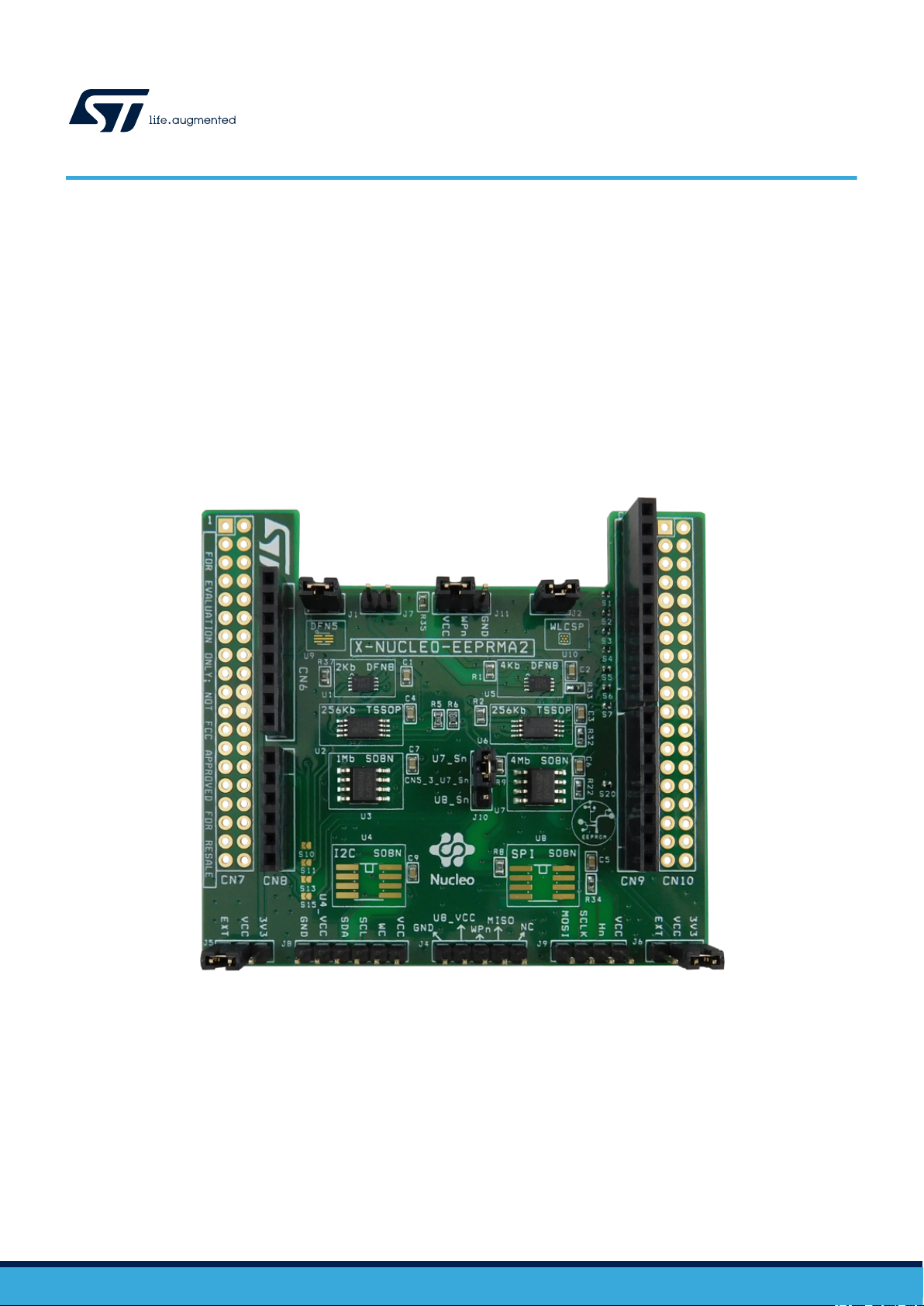
The X-NUCLEO-EEPRMA2 expansion board is designed for M24xx series I²C and M95xx series SPI EEPROM for data reading
and writing.
The expansion board acts as an external storage device that can be used to store data such as manufacturing traceability,
calibration, user settings, error flags, data logs and monitoring data to make applications more flexible and accurate.
The X-NUCLEO-EEPRMA2 expansion board is compatible with the Arduino UNO R3 connector pin assignment and can be
easily plugged to any STM32 Nucleo development board. You can mount the ST morpho connectors if required.
Figure 1. X-NUCLEO-EEPRMA2 expansion board
UM2665 - Rev 3 - August 2020
For further information contact your local STMicroelectronics sales office.
www.st.com

1 Acronyms and abbreviations
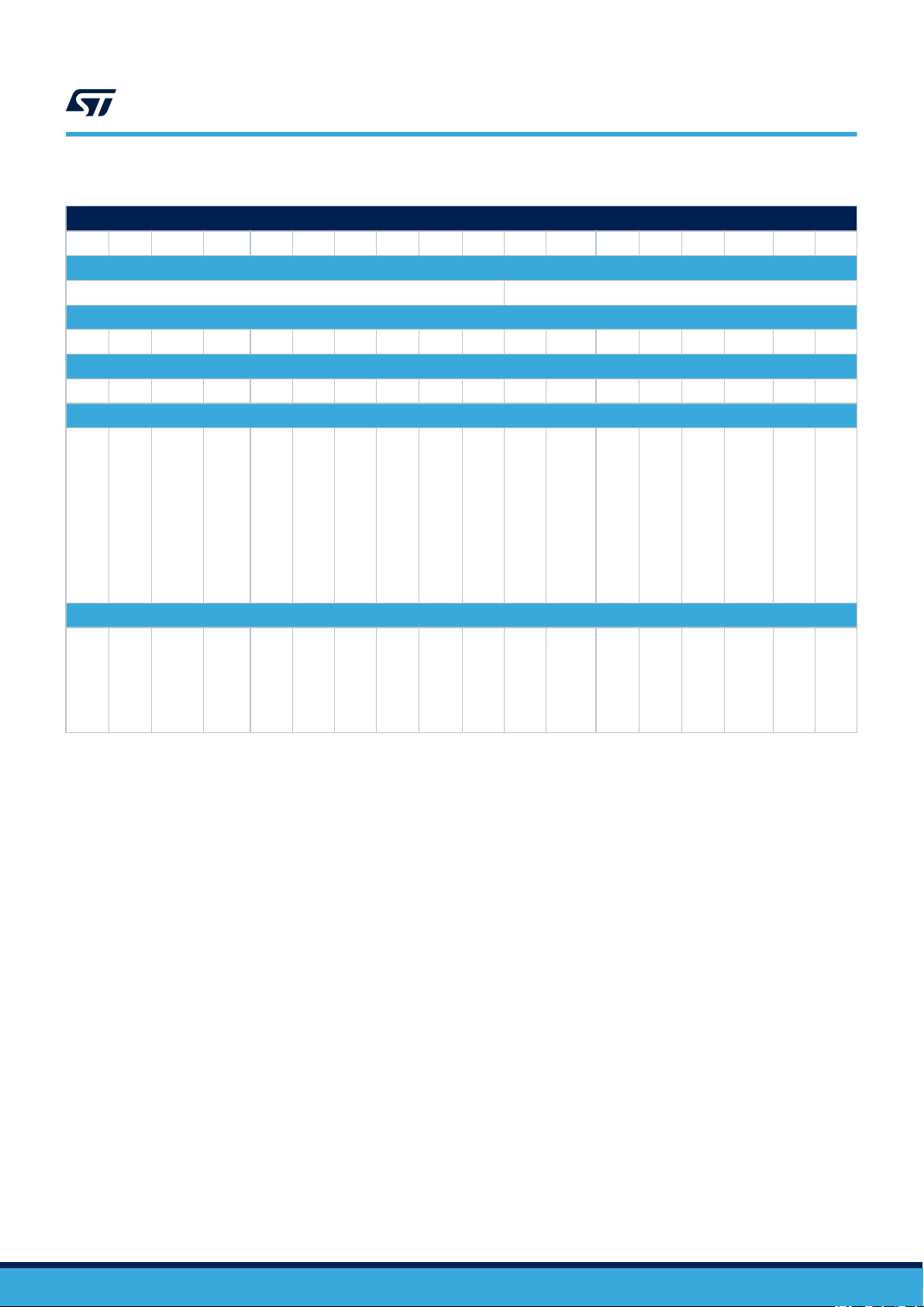
Table 1. List of acronyms
Acronym Description
EEPROM Electrically erasable programmable read only memory
MHz Mega Hertz
MCU Microcontroller unit
SPI Serial peripheral interface
I2C Inter-integrated circuit
UM2665
Acronyms and abbreviations
UM2665 - Rev 3
page 2/23

2 Getting started
2.1 Overview
The X-NUCLEO-EEPRMA2 main features are:
• Up to 1-Mbit serial I²C bus embedded EEPROM
• Up to 4-Mbit SPI bus embedded EEPROM
• Easy portability across different MCU families
• Equipped with Arduino™ UNO R3 connector
• Compatible with STM32 Nucleo boards
• Free comprehensive development firmware library and sample implementation available when the X-
NUCLEO-EEPRMA2 expansion board is plugged on top of a NUCLEO-F401RE or NUCLEO-L053R8
development board
• Developer can choose and solder an EEPROM to be tested using the evaluation software provided
2.2 Typical applications
The X-NUCLEO-EEPRMA2 expansion board acts as an external storage device that can be used for storing data
such as manufacturing traceability, calibration data, user setting, error flags, data log and monitoring data to make
applications more flexible and accurate.
UM2665
Getting started
UM2665 - Rev 3
page 3/23
2.3 Hardware requirements
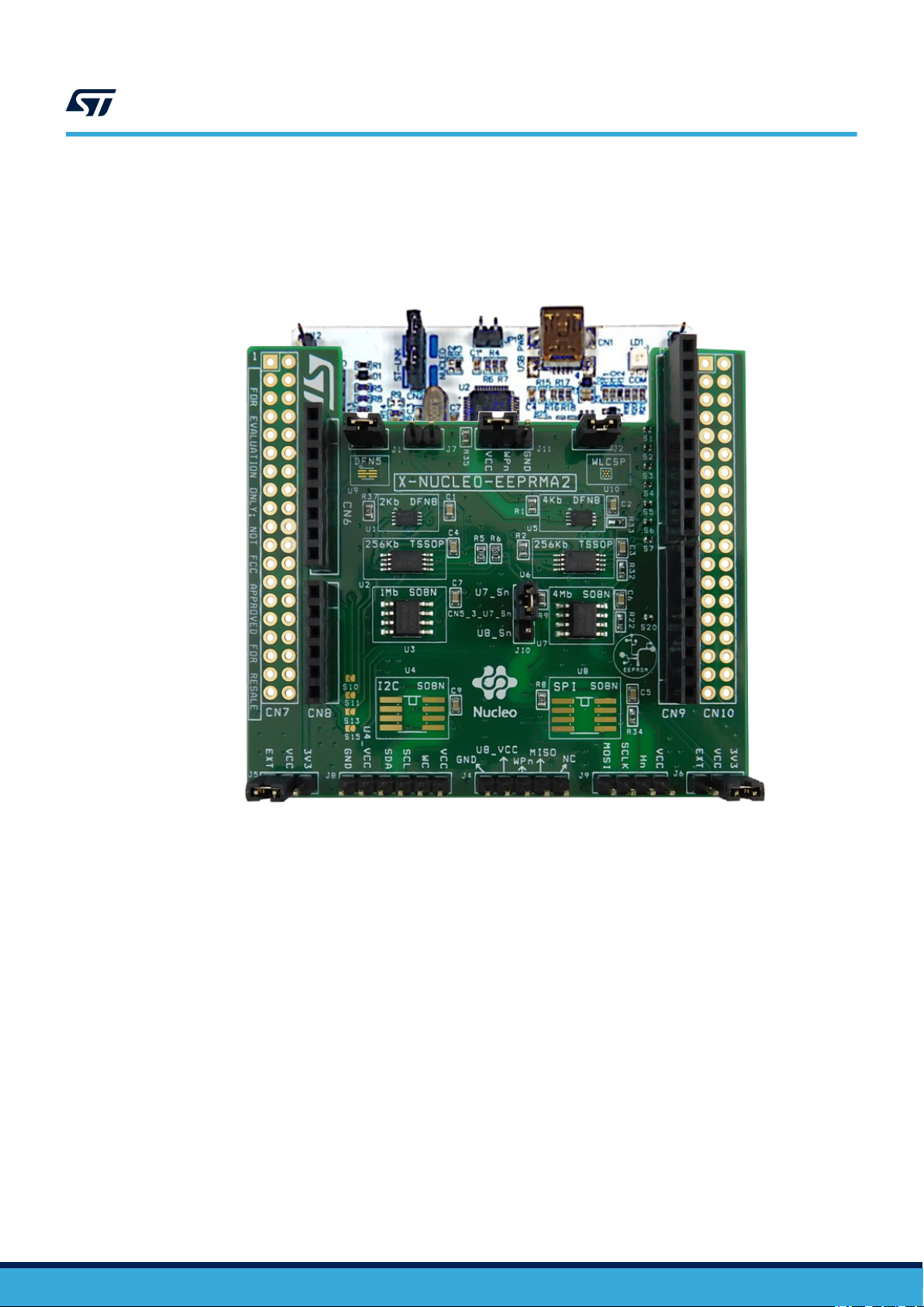
To use STM32 Nucleo development boards with the X-NUCLEO-EEPRMA2 expansion board, connect the boards
as shown below.
Figure 2. X-NUCLEO-EEPRMA2 expansion board connected to an STM32 Nucleo development board
UM2665
Hardware requirements
2.4
2.5
UM2665 - Rev 3
The EEPROM communicates with the STM32 Nucleo development board host microcontroller through the SPI or
I²C signals available on the Arduino UNO R3 connector.
The X-NUCLEO-EEPRMA2 has been designed to allow using any STM32 Nucleo board, although complete
testing has been performed using the NUCLEO-F401RE and NUCLEO-L053R8 boards.
System requirements
To use the STM32 Nucleo development boards with the X-NUCLEO-EEPRMA2 expansion board you need:
• a Windows PC/laptop (Windows 7 or above) to install the firmware package (X-CUBE-EEPRMA1)
• a type A to Mini-B USB cable to connect the STM32 Nucleo board to the PC
• an STM32 Nucleo development board (NUCLEO-F401RE or NUCLEO-L053R8)
• an X-NUCLEO-EEPRMA2 expansion board
Board setup
Step 1. Check the jumper on J1 and J2 connectors are connected.
These jumpers provide the required voltage to the devices.
Step 2. Ensure jumper on J11 is put between VCC and WPn.
Step 3. Ensure jumper on J10 is put between U7_Sn and CN5_3_U7_Sn.
page 4/23

Step 4. Connect the X-NUCLEO-EEPRMA2 to the STM32 Nucleo board as shown in Figure 2.
Step 5. Power the STM32 Nucleo development board using the Mini-B USB cable.
Step 6. Program the firmware in the development board.
Step 7. Reset the MCU board using the reset button on the STM32 Nucleo development board.
The evaluation kit is ready-to-use.
UM2665
Board setup
UM2665 - Rev 3
page 5/23
UM2665
Hardware description and configuration
3 Hardware description and configuration
3.1 Interconnection details
The X-NUCLEO-EEPRMA2 expansion board and the NUCLEO-L053R8 or NUCLEO-F401RE board connection
details are listed below.
Table 2. X-NUCLEO-EEPRMA2 and NUCLEO-L053R8 connection details (left connector)
Signal name
NC IOREF RESET 3V3 5V GND GND VIN A0 A1 A2 A3 A4 A5
Connector name
CN6 Power CN8 Analog
Pin number
1 2 3 4 5 6 7 8 1 2 3 4 5 6
NUCLEO-L053R8 MCU port
NRST PA0 PA1 PA4 PB0 PC1/PB9 PC0/PB8
NUCLEO-L053R8 MCU signals
3.3 V
RESET
REF
NC 3V3 GND GND M95_WPn M24_VCC M95_Hn U8_Sn
3.3 V
input/
output
5 V
output
GND GND
POWER
INPUT
X-NUCLEO-EEPRMA2 expansion board signals
ADC_IN0 ADC_IN1 ADC_IN4 ADC_IN8
ADC_IN11(PC1)
or
I2C1_SDA(PB9)
ADC_IN10(PC0)
or
I2C1_SCL(PB8)
UM2665 - Rev 3
page 6/23
UM2665
Interconnection details
Table 3. X-NUCLEO-EEPRMA2 and NUCLEO-L053R8 connection details (right connector)
Signal name
D15 D14 AREF GND D13 D12 D11 D10 D9 D8 D7 D6 D5 D4 D3 D2 D1 D0
Connector name
CN5 Digital CN9 Digital
Pin number
10 9 8 7 6 5 4 3 2 1 8 7 6 5 4 3 2 1
NUCLEO-L053R8 MCU port
PB8 PB9 PA5 PA6 PA7 PB6 PC7 PA9 PA8 PB10 PB4 PB5 PB3 PA10 PA2 PA3
NUCLEO-L053R8 MCU signals
I2C_SCL
I2C_SDA
M24_I2C_SCL
M24_I2C_SDA
AVDD
GND
GND
SPI1_SCK
SPI1_MISO
M95_MISO
M95_SCLK
SPI1_CS
TIM12_CH2
TIM12_CH2 SPI1_MOSI
X-NUCLEO-EEPRMA2 shield signals
M95_MOSI
U6_Sn
CN5_3_U7_Sn
TIM2_CH3
TIM12_CH1
TIM2_CH2
U5_Sn
USART2_TX
Table 4. X-NUCLEO-EEPRMA2 and NUCLEO-F401RE connection details (left connector)
Signal name
NC IOREF RESET 3V3 5V GND GND VIN A0 A1 A2 A3 A4 A5
Connector name
CN6 Power CN8 Analog
Pin number
1 2 3 4 5 6 7 8 1 2 3 4 5 6
NUCLEO-F401RE MCU port
NRST PA0 PA1 PA4 PB0 PC1 PC0
NUCLEO-F401RE MCU signals
3.3 V
RESET
REF
NC 3V3 GND GND M95_WPn M24_VCC M95_Hn U8_Sn
3.3 V
input/
output
5 V
output
GND GND
POWER
INPUT
X-NUCLEO-EEPRMA2 expansion board signals
ADC1_0 ADC1_1 ADC1_4 ADC1_8
ADC1_11(PC1)
or
I2C1_SDA(PB9)
ADC1_10(PC0)
or
I2C1_SCL(PB8)
USART2_RX
UM2665 - Rev 3
page 7/23
UM2665
Current measurement
Table 5. X-NUCLEO-EEPRMA2 and NUCLEO-F401RE connection details (right connector)
Signal name
D15 D14 AREF GND D13 D12 D11 D10 D9 D8 D7 D6 D5 D4 D3 D2 D1 D0
Connector name
CN5 Digital CN9 Digital
Pin number
10 9 8 7 6 5 4 3 2 1 8 7 6 5 4 3 2 1
NUCLEO-F401RE MCU port
PB8 PB9 PA5 PA6 PA7 PB6 PC7 PA9 PA8 PB10 PB4 PB5 PB3 PA10 PA2 PA3
NUCLEO-F401RE MCU signals
I2C1_SCL
I2C1_SDA
M24_I2C_SCL
M24_I2C_SDA
AVDD
GND
GND
SPI1_SCK
SPI1_MISO
M95_MISO
M95_SCLK
3.2 Current measurement
J1 can be used to monitor the I²C device power consumption, whereas J2 can be used to monitor the SPI device
power consumption. Connect an ammeter probe between the connector pin 1 and pin 2 for measurements.
TIM3_CH2
TIM4_CH4 SPI1_CS
TIM1_CH1N SPI1_MOSI
X-NUCLEO-EEPRMA2 shield signals
M95_MOSI
U6_Sn
CN5_3_U7_Sn
TIM2_CH3
TIM3_CH1
TIM2_CH2
U5_Sn
USART2_TX
USART2_RX
UM2665 - Rev 3
page 8/23

X-NUCLEO-EEPRMA2 component placement details
3.3 X-NUCLEO-EEPRMA2 component placement details
Figure 3. X-NUCLEO-EEPRMA2 component placement details
UM2665
Figure 4. X-NUCLEO-EEPRMA2 top view layout
UM2665 - Rev 3
page 9/23

X-NUCLEO-EEPRMA2 component placement details
Figure 5. X-NUCLEO-EEPRMA2 bottom view layout
UM2665
UM2665 - Rev 3
page 10/23

4 Component description
4.1 M24XX
Feature Description
Sales type M24C02-FMC6TG
Package UFDFPN8
Single supply voltage 1.7 to 5.5 V (full temperature range) and 1.6 to 1.7 V (limited temperature range)
Feature Description
Sales type M24256-DFDW6TP
Package TSSOP8
Single supply voltage and high speed 1 MHz clock from 1.7 to 5.5 V
UM2665
Component description
Table 6. M24C02 details
Table 7. M24256 details
Sales type M24M01-DFMN6TP
Package SO8
Single supply voltage and high speed 1 MHz clock from 1.7 to 5.5 V
4.2 M95XX
Sales type M95040-RMC6TG
Package UFDFPN8
Single supply voltage 1.7 to 5.5 V
Sales type M95256-DFDW6TP
Package TSSOP8
Single supply voltage 1.7 to 5.5 V
Table 8. M24M01 details
Feature Description
Table 9. M95040 details
Feature Description
Table 10. M95256 details
Feature Description
UM2665 - Rev 3
page 11/23

Table 11. M95M04 details
Feature Description
Sales type M95M04-DRMN6TP
Package SO8
Single supply voltage 1.8 to 5.5 V
UM2665
M95XX
UM2665 - Rev 3
page 12/23

5 External EEPROMs
External SPI EEPROM
You can easily solder a specific EEPROM density I²C or SPI to be used with the X-NUCLEO-EEPRMA2
expansion board. The software can handle any density between 2 Kbit and 4 Mbits.
To use the external EEPROM, you have to apply some changes to the firmware and the hardware, as described
below.
Step 1. Uncomment the macro M24XX (to use the I²C EEPROM) or M95XX (to use the SPI EEPROM) in the
“eeprom_expansion.h” file
Step 2. Comment the macro I²C (to use the external I²C EEPROM) or the macro SPI (to use the external SPI
EEPROM).
Step 3. Open J5 and J6 3V3 and VCC pins and short the EXT and VCC pins
Note: External VCC can be used to power EEPROM with a different VCC for specific evaluations.
Figure 6. I2C and SPI EEPROM soldered on the X-NUCLEO-EEPRMA2 expansion board
UM2665
External EEPROMs
UM2665 - Rev 3
page 13/23
6 Bill of materials
Item Q.ty Ref. Part / Value Description Manufacturer Order code
1 1 U1
2 1 U2
3 1 U3
4 1 U5
5 1 U6
6 1 U7
7 2 U4, U8 SO8 Not mounted Any
8 1 U9 UFDFPN5 Not mounted Any
9 1 U10 WLCSP Not mounted Any
8 1 CN5
9 2 CN6, CN9
10 2 CN7, CN10
11 1 CN8
12 8
13 2 J1, J2 2 pin male strip Jumpers Any
14 1 J4 5 pin male strip Jumpers Any
15 4
16 1 J7
17 1 J9 4 pin male strip Jumpers Any
18 1 J8 6 pin male strip Jumpers Any
19 5
20 2 R5, R6
21 1 R37
C1, C2, C3,
C4, C5, C6,
C7, C9
J5, J6, J10,
J11
R1, R2, R8,
R9, R35
Table 12. X-NUCLEO-EEPRMA2 bill of materials
2 KBIT 400 KHZ
UFDFPN8
256 KBIT 1 MHZ
TSSOP8
1 MBIT 1 MHZ
SO8
4 KBIT 5 MHZ
UFDFPN8
256 KBIT 20 MHZ
TSSOP8
4 MBIT 10 MHZ
SO8
10 pin female-male
strip, 2.54 mm
pitch
8 pin female-male
strip, 2.54 mm
pitch
19x2 through hole,
2.54 mm pitch
6 pin female-male
strip, 2.54 mm
pitch
100 nF 25 V ±10%
X7R SMD0603
3 pin male strip Jumpers Any
open - 2 pin male
strip
10 K ±5% 1/10 W
SMD0603
3.3 K ±5% 1/10 W
SMD0603
1 kohm ±5% 1/10
W SMD0603
2-Kbit serial I²C bus
EEPROM
256-Kbit serial I²C
bus EEPROM
1-Mbit serial I²C bus
EEPROM
4-Kbit SPI bus
EEPROM with highspeed clock
256-Kbit serial SPI
bus EEPROM with
high speed clock
4-Mbit serial SPI bus
EEPROM
Header Samtec ESQ-110-24-T-S
Header Samtec ESQ-108-24-T-S
Header Samtec ESQ-119-24-T-S
Header Samtec ESQ-108-24-T-S
Ceramic capacitor Murata GRM188R71E104KA01D
Jumpers Any
Resistors Panasonic ERJ-3GEYJ103V
Resistors Yageo RC0603JR-073K3L
Resistors Panasonic ERJ-3GEYJ102V
ST M24C02-FMC6TG
ST M24256-DFDW6TP
ST M24M01-DFMN6TP
ST M95040-RMC6TG
ST M95256-DFDW6TP
ST M95M04-DRMN6TP
UM2665
Bill of materials
UM2665 - Rev 3
page 14/23

Item Q.ty Ref. Part / Value Description Manufacturer Order code
22 4
23 8
24 2 S11, S15 OPEN Solder bridge Any
25 2 S10, S13 OPEN Solder bridge Any
R22, R32,
R33, R34
S1, S2, S3,
S4, S5, S6,
S7, S20
10 K ±5% 1/10 W
SMD0402
CLOSE Solder bridge Any
Resistors Panasonic ERJ-2GEJ103X
UM2665
Bill of materials
UM2665 - Rev 3
page 15/23

M95_MOSI
C2
D
3
4
VWSS
5
J11
M95M04-DRMN6TP
M95_VCC
U6
10K
M95_VCC
3V3
U8_EXT_SUPPLY
A3
J6
100nF
3
4
VWSSD
5
10K
M95_SCLK
CON3
10K
U6_Sn
C
6
3V3
2
9
Ex.PAD
M95_Hn
M95_MISO
M95_SCLK
C
6
1
2
3
J4
HOLD
VCC
8
M95_Hn
U9
EEPROM_WLCSP
M95_VCC
7
HOLD
M95_WPn
U8_VCC
A1
M95_SCLK
CON5
7
HOLD
U5_Sn
M95_Hn
M95_VCC
FOR CURRENT MEASUREMENT
R1
CON3
Q
2
C1
C5
U10
VCC
8
7
M95_VCC
M95_MISO
CN5_3_U7_Sn
U8_Sn
E15
2
4
1
2
3
4
M95_Hn
U8_VCC
10K
M95256-DFDW6TP
S
1
1
2
3
M95_VCC
CON3
10K
R34
100nF
M95_MISO
EEPROM_UFDFPN5
U8_VCC
(4Kb, DFN8 )
(256Kb, TSSOP)
(4Mb, SO8N)
EEPROM_SPI_SO8N
U8_VCC
M95_VCC
R2
M95_VCC
M95_VCC
M95_VCC
M95_WPn
C3
J10
1
2
S
Q
S
1
B2
R22
10K
M95_MOSI
1
2
3
4
5
C
6
M95_VCC
U8
M95_MOSI
M95_MISO
2
3
Q
W
VSS
4
R8
U7
R9
HOLD
8
VCC
M95_MISO
D
5
C3
C6
10K
C
6
M95040-RMC6TG
3
4
VWSSD
5
100nF
10K
1
2
S
Q
M95_SCLK
U5
U7_Sn
M95_WPn
J9
M95_WPn
U8_Sn
1
D2
10K
M95_VCC
1
2
3
M95_Hn
1
2
3
7
M95_MOSI
R33
R35
M95_WPn
E3
M95_WPn
R32
100nF
J2
M95_VCC
M95_MOSI
U7_Sn
8
VCC
M95_SCLK
UM2665 - Rev 3
7 Schematic diagrams
Figure 7. X-NUCLEO-EEPRMA2 circuit schematic (1 of 4)
page 16/23
Schematic diagrams
UM2665

M24_I2C_SCL
M24_WC
WC
7
9
Ex.PAD
M24_VCC
U1
1
(2Kb, DFN8 )
(256Kb, TSSOP)
(1Mb, SO8N)
EEPROM_I2C_SO8N
FOR CURRENT MEASUREMENT
3V3
M24_WC
M24_WC
100nF
M24_VCC
1K R37
M24_WC
U3
M24_WC
5
3
OPEN
5
VSSSDA
SCL
6
2
3.3K
M24_VCC
C7
M24_I2C_SDA
VSSSDA
SCL
6
M24_I2C_SDA
M24_I2C_SCL
3V3
VSS SDA
6
SCL
M24_I2C_SCL
M24_I2C_SDA
E1
2
U4
JJ11
R5
U2
4
M24M01-DFMN6TP
M24_VCC
5
M24_VCC
E0
1
M24_WC
5
JJ88
C4
M24256-DFDW6TP
R6
J5
M24_VCC
U4_VCC
M24C02-FMC6TG
1
U4_VCC
U4_EXT_SUPPLY
3.3K
2
3
EE1
2
4
1
2
3
4
5
6
VCC
8
100nF
M24_I2C_SCL
CON6
1
2
EE0
1
E2
3
WC
7
WC
7
VCC
8
2
3
EE1
2
4
CC11
M24_I2C_SCL
100nF
M24_I2C_SDA
VCC
8
4
EV2
SSSDA
SCL
6
1
2
3
CON3
2
DU
1
J7
8
VCC
100nF
C9
M24_I2C_SCL
M24_I2C_SDA
M24_VCC
M24_I2C_SDA
U4_VCC
WC
7
M24_VCC
M24_VCC
E0
1
M24_VCC
M24_VCC
UM2665 - Rev 3
Figure 8. X-NUCLEO-EEPRMA2 circuit schematic (2 of 4)
page 17/23
Schematic diagrams
UM2665

21
27
38
25
2
4
6
8
1
12
24
30
3V3
5V
31
RESET
1817
A5
14
D1
D0
35
CN7
36
26
23
D8
1
3
5
7
9
AREF
D6
17
A0
16
A2
A3
D4
13
SCL
D2
Vin
29
1
3
5
7
9
11
30
32
34
12
29
20
21
13
15
D13
28
22
0
33
26
3V3
19
34
CN10
22
D10
D9
0
15
31
33
D12
D7
A4
28
D5
14
24
SDA
35
37
D3
A1
37
2
4
6
8
1
36
38
27
D11
16
18
23
25
32
20
11
19
S15
2
D0
S1
S10
A3
4
3
S20
A5
6
D1
SCL
10
A5
TXD/D1
D2
3
CN8
A4
A2
S2
GND
7
S3
CLOSED
U8_Sn
M95_MISO
M95_Hn
AREF
9
SDA
2
A4
5
U5_Sn
S13
D4
5
S7
GND
6
CLOSED
MOSI/PWM/D11
5
8
A0
D7
D6
M24_WC
S5
IOREF
AREF
A0
1
D3
4
CN6
VIN
8
MISO/D12
6
D12
D13
A1
A3
D8
S4
D9
D11
D6
7
CN5_3_U7_Sn
SCK/D13
GND
7
M24_I2C_SDA
RESET
M24_I2C_SCL
M95_MOSI
D5
6
A2
3
OPEN
D2
4
3V3
PWM/D10
4
D7
8
D8
1
5V
CN5
S6
RXD/D0
2
D3
A1
2
5V
5
M95_WPn
3V3
NC
1
Vin
M95_SCLK
D10
U6_Sn
S11
1
D5
D4
CN9
RESET
PWM/D9
3
OPEN
OPEN
OPEN
CLOSED
CLOSED
CLOSED
CLOSED
CLOSED
CLOSED
SCL
SDA
UM2665 - Rev 3
Figure 9. X-NUCLEO-EEPRMA2 circuit schematic (3 of 4)
Figure 10. X-NUCLEO-EEPRMA2 circuit schematic (4 of 4)
page 18/23
Schematic diagrams
UM2665

Revision history
Date Revision Changes
03-Dec-2019 1 Initial release.
27-Feb-2020 2
28-Aug-2020 3 Updated Section 2.1 Overview.
UM2665
Table 13. Document revision history
Updated Figure 1. X-NUCLEO-EEPRMA2 expansion board and Figure 2. X-NUCLEO-EEPRMA2
expansion board connected to an STM32 Nucleo development board.
UM2665 - Rev 3
page 19/23

UM2665
Contents
Contents
1 Acronyms and abbreviations ......................................................2
2 Getting started ....................................................................3
2.1 Overview .....................................................................3
2.2 Typical applications.............................................................3
2.3 Hardware requirements .........................................................4
2.4 System requirements ...........................................................4
2.5 Board setup ...................................................................4
3 Hardware description and configuration ...........................................6
3.1 Interconnection details ..........................................................6
3.2 Current measurement...........................................................8
3.3 X-NUCLEO-EEPRMA2 component placement details ................................9
4 Component description ...........................................................11
4.1 M24XX ......................................................................11
4.2 M95XX ......................................................................11
5 External EEPROMs ...............................................................13
6 Bill of materials...................................................................14
7 Schematic diagrams ..............................................................16
Revision history .......................................................................19
UM2665 - Rev 3
page 20/23

UM2665
List of tables
List of tables
Table 1. List of acronyms ....................................................................2
Table 2. X-NUCLEO-EEPRMA2 and NUCLEO-L053R8 connection details (left connector) .......................6
Table 3. X-NUCLEO-EEPRMA2 and NUCLEO-L053R8 connection details (right connector) ......................7
Table 4. X-NUCLEO-EEPRMA2 and NUCLEO-F401RE connection details (left connector) .......................7
Table 5. X-NUCLEO-EEPRMA2 and NUCLEO-F401RE connection details (right connector) ......................8
Table 6. M24C02 details .................................................................... 11
Table 7. M24256 details .................................................................... 11
Table 8. M24M01 details .................................................................... 11
Table 9. M95040 details .................................................................... 11
Table 10. M95256 details .................................................................... 11
Table 11. M95M04 details .................................................................... 12
Table 12. X-NUCLEO-EEPRMA2 bill of materials .................................................... 14
Table 13. Document revision history .............................................................19
UM2665 - Rev 3
page 21/23

UM2665
List of figures
List of figures
Figure 1. X-NUCLEO-EEPRMA2 expansion board ..................................................1
Figure 2. X-NUCLEO-EEPRMA2 expansion board connected to an STM32 Nucleo development board .............4
Figure 3. X-NUCLEO-EEPRMA2 component placement details .........................................9
Figure 4. X-NUCLEO-EEPRMA2 top view layout ...................................................9
Figure 5. X-NUCLEO-EEPRMA2 bottom view layout................................................ 10
Figure 6. I2C and SPI EEPROM soldered on the X-NUCLEO-EEPRMA2 expansion board ..................... 13
Figure 7. X-NUCLEO-EEPRMA2 circuit schematic (1 of 4)............................................ 16
Figure 8. X-NUCLEO-EEPRMA2 circuit schematic (2 of 4)............................................ 17
Figure 9. X-NUCLEO-EEPRMA2 circuit schematic (3 of 4)............................................ 18
Figure 10. X-NUCLEO-EEPRMA2 circuit schematic (4 of 4)............................................ 18
UM2665 - Rev 3
page 22/23

UM2665
IMPORTANT NOTICE – PLEASE READ CAREFULLY
STMicroelectronics NV and its subsidiaries (“ST”) reserve the right to make changes, corrections, enhancements, modifications, and improvements to ST
products and/or to this document at any time without notice. Purchasers should obtain the latest relevant information on ST products before placing orders. ST
products are sold pursuant to ST’s terms and conditions of sale in place at the time of order acknowledgement.
Purchasers are solely responsible for the choice, selection, and use of ST products and ST assumes no liability for application assistance or the design of
Purchasers’ products.
No license, express or implied, to any intellectual property right is granted by ST herein.
Resale of ST products with provisions different from the information set forth herein shall void any warranty granted by ST for such product.
ST and the ST logo are trademarks of ST. For additional information about ST trademarks, please refer to www.st.com/trademarks. All other product or service
names are the property of their respective owners.
Information in this document supersedes and replaces information previously supplied in any prior versions of this document.
© 2020 STMicroelectronics – All rights reserved
UM2665 - Rev 3
page 23/23
 Loading...