

Page 1
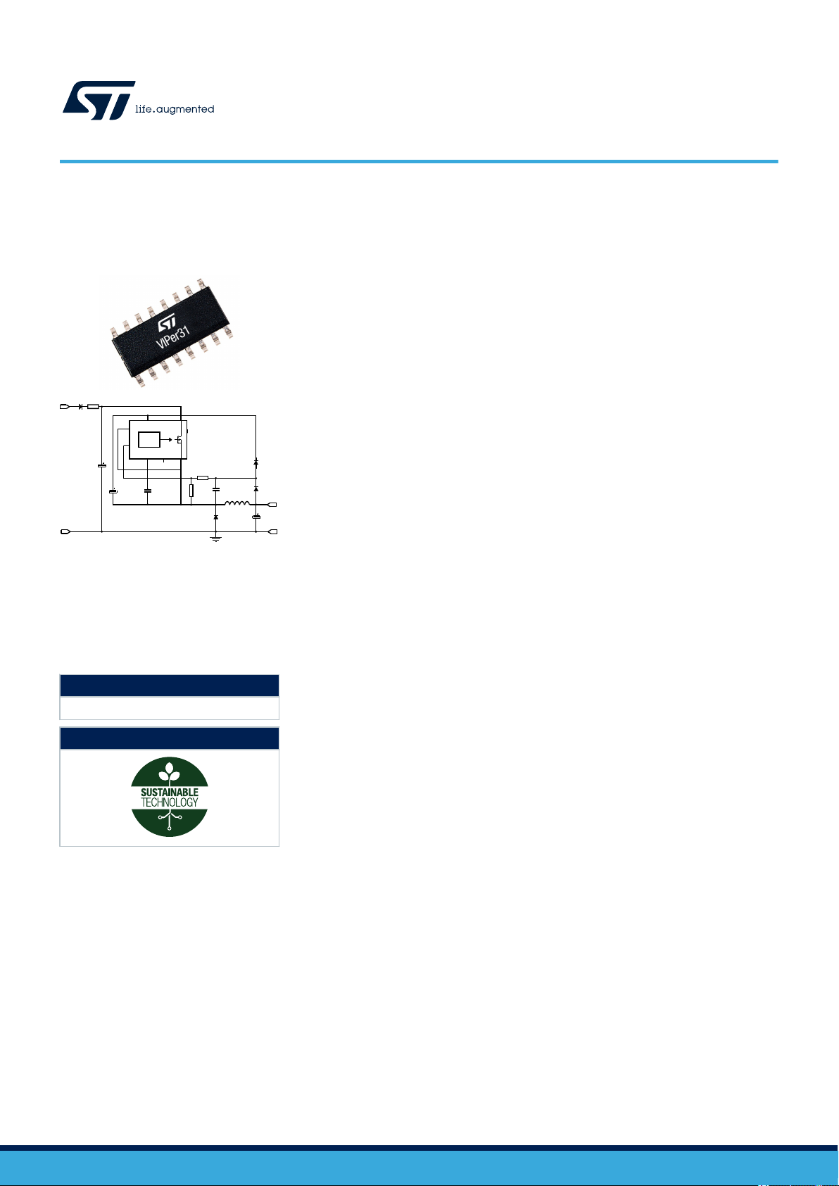
DRAIN
GND
VCC
UVPCOMP
CONTROL
FB
OVP
GND
V
OUT
C
OUT
R2
R1
C2
GND
C
IN
~ AC
R
IN
D
IN
VIPER31
C1
D
AUX
D1
L
OUT
D2
C3
Product status link
VIPER31
Product label
VIPER31
Datasheet
Energy saving offline high voltage converter
Features
• 800 V avalanche-rugged power MOSFET to cover ultra-wide VAC input range
• Embedded HV startup and sense FET
• Current mode PWM controller
• Drain current limit protection (OCP):
– 850 mA (VIPER318)
– 990 mA (VIPER319)
• Wide supply voltage range: 4.5 V to 30 V
– < 20 mW @ 230 VAC in no-load;
– < 430 mW @ 230 VAC, 25 0mW output load
• Jittered switching frequency reduces the EMI filter cost:
– 30 kHz ± 7% (X type)
– 60 kHz ± 7% (L type)
– 132 kHz ±7% (type H)
• Embedded E/A with 1.2 V reference
• Built-in soft-start for improved system reliability
• Protections with automatic restart:
– overload/short-circuit (OLP)
– thermal shutdown
– overvoltage
• Protections without automatic restart:
– pulse-skip protection to avoid flux runaway
– undervoltage/disable
– max. duty cycle
Application
• Low power SMPS for home appliances, home automation, industrial,
consumers, lighting
• Low power adapters
Description
The VIPER31 device is a high-voltage converter that smartly integrates an 800 V
avalanche rugged power MOSFET with PWM current-mode control..
The 800 V breakdown allows extended input voltage range to be applied, as well as
to reduce the size of the DRAIN snubber circuit. The IC can meet the most stringent
energy-saving standards as it has very low consumption and operates in pulse
frequency modulation at light load. Overvoltage and undervoltage protections with
separate and settable intervention thresholds are available at OVP and UVP pins
respectively. UVP can also be used as a disabling input for the entire SMPS, with
ultra-low residual input power consumption. Integrated HV startup, sense FET, error
DS13285 - Rev 2 - June 2020
For further information contact your local STMicroelectronics sales office.
amplifier and oscillator with frequency jitter allow a complete application to be
designed with a minimum component count.
Flyback, buck and buck boost topologies are supported.
www.st.com
Page 2

1 Pin setting
GND
N.C.
OVP
N. A.
UVP
VCC
N. C.
N. C.
N. C.
N. C.
DRAIN
DRAIN
DRAIN
DRAIN
FB
COMP
VIPER31
Pin setting
Figure 1. Connection diagram
Table 1. Pin description
Pin
number
1 GND
2 N. C. Not connected. When designing the PCB, this pin can be soldered to GND.
3 VCC
4 N.A.
5 UVP
6 OVP
7
Name Function
Ground and MOSFET source. Connection of both the source of the internal MOSFET and the return of
the bias current of the device. All of the groundings of bias components must be tied to a trace going to
this pin and kept separate from the pulsed current return.
Controller Supply. An external storage capacitor has to be connected across this pin and GND. The
pin, internally connected to the high-voltage current source, provides the VCC capacitor charging current
at startup. A small bypass capacitor (0.1 μF typ.) in parallel, placed as close as possible to the IC, is also
recommended, for noise filtering purposes.
Not available for user. This pin is mechanically connected to the controller die pad of the frame. In order
to improve noise immunity, it is highly recommended to connect it to GND.
FB
Undervoltage Protection. If V
t
V
switching. The pin can be used to realize an input undervoltage protection or as a disabling input for the
entire SMPS, with ultra-low residual input power consumption. If the feature is not required, the pin must
be left open, which excludes the function.
Overvoltage protection. If VOVP exceeds the internal threshold V
t
the OVP condition is removed, after that it restarts switching with soft-start phase. OVP pin can be used
to realize an input overvoltage protection (or, in non-isolated topologies, an output overvoltage
protection).
If the feature is not required, the pin must be connected to GND, which excludes the function.
Direct feedback. It is the inverting input of the internal transconductance E/A, internally referenced to
1.2 V with respect to GND. In non-isolated converter, the output voltage information is directly fed into the
pin through a voltage divider. In primary regulation, the FB voltage divider is connected to the VCC. The
E/A is disabled if FB is connected to GND pin.
time (30 ms, typ.), the IC is disabled, and its consumption reduced to ultra-low values. When
UVP_DEB
rises above V
UVP
time (250 μsec, typ.), the PWM is disabled in auto-restart for t
OVP_DEB
UVP_th,
falls below the internal threshold V
UVP
the device waits for a t
UVP_REST
UVP_th
time interval (30 ms, typ.) then resumes
(4 V typ.) for more than
OVP_th
OVP_REST
(0.4 V typ.) for more than
(500 msec, typ.) until
DS13285 - Rev 2
page 2/40
Page 3

VIPER31
Pin setting
Pin
number
8 COMP
9 to 12 N.C. Not connected. These pins must be left floating in order to get a safe clearance distance.
13 to 16 DRAIN
Name Function
Compensation. This is the output of the internal E/A. A compensation network is placed between this
pin and GND to achieve stability and good dynamic performance of the control loop. In case of
secondary feedback, the internal E/A must be disabled and the COMP directly driven by the optocoupler
to control the DRAIN peak current setpoint.
MOSFET drain. The internal high-voltage current source sources current from these pins to charge the
VCC capacitor at startup. The pins are mechanically connected to the internal metal PAD of the
MOSFET in order to facilitate heat dissipation. On the PCB, some copper areas under these pins
decreases the total junction-to-ambient thermal resistance thus facilitating the power dissipation.
DS13285 - Rev 2
page 3/40
Page 4
2 Electrical and thermal ratings
Table 2. Absolute maximum ratings
Symbol
V
I
DRAIN
V
V
V
V
V
P
T
T
DS
CC
OVP
UVP
FB
COMP
TOT
J
STG
Drain-to- source (ground) voltage 800 V
Pulsed drain current (pulse-width limited by SOA) 3 A
VCC voltage -0.3 30.5V V
OVP voltage -0.3
UVP voltage -0.3
FB voltage -0.3
COMP voltage -0.3
Power Dissipation @ Tamb < 50°C
Junction Temperature operating range -40 150 °C
Storage Temperature -55 150 °C
1. stresses beyond those listed absolute maximum ratings may cause permanent damage to the device.
2. exposure to absolute-maximum-rated conditions for extended periods may affect the device reliability
3. by internal clamp between 4.75 V and 5.25 V or Vcc + 0.6 V, whichever is lower
4. the AMR value is intended when VCC ≥ 5 V, otherwise the value VCC + 0.3 V has to be considered.
5. when mounted on a standard single side FR4 board with 100 mm² (0.155² inch) of Cu (35 μm thick)
Parameter
(1)(2)
VIPER31
Electrical and thermal ratings
Min. Max. Unit
Internally
limited
Internally
limited
(4)
5
Internally
limited
(5)
1
V
(3)
V
(3)
V
V
(3)
W
Table 3. Thermal data
Parameter
(1)
(1)
(2)
(2)
R
R
R
R
Symbol
TH-JC
TH-JA
TH-JC
TH-JA
Thermal resistance junction to case
(dissipated power = 1W)
Thermal resistance junction to ambient
(dissipated power = 1W)
Thermal resistance junction to case
(dissipated power = 1W)
Thermal resistance junction to ambient
(dissipated power = 1W)
1. when mounted on a standard single side FR4 board with minimum copper area
2. when mounted on a standard single side FR4 board with 100mm² (0.155² inch) of Cu (35 μm thick)
Max. value
SO16N
10 °C/W
120 °C/W
5 °C/W
85 °C/W
Unit
DS13285 - Rev 2
page 4/40
Page 5

0.750
0.875
1.000
1.125
1.250
1.375
1.500
0 25 50 75 100 125 150 175 200 225
A (mm2)
R
thJA
/(R
thJA
@ A = 100mm2)
VIPER31
Electrical characteristics
Figure 2. R
versus copper area
th_JA
Table 4. Avalanche characteristics
2.1
Symbol
I
AR
EAS
1. Parameter derived by characterization
Avalanche current
Single pulse avalanche energy
Electrical characteristics
Parameter Condition Min. Typ. Max. Unit
Repetitive and non-repetitive.
Pulse-width limited by T
Jmax
1.15 A
IAS = IAR,
(1)
V
DS
= 100 V,
3 mJ
Starting TJ = 25°C
Tj = -40 to 125°C, VCC = 9 V (unless otherwise specified)
Symbol
V
BVDSS
I
DSS
I
OFF
R
DS(on)
Parameter
Breakdown voltage
Drain-source leakage current
OFF state drain current
Static drain-source
ON‑resistance
Table 5. Power section
Test condition Min. Typ. Max. Unit
I
= 1 mA, V
DRAIN
TJ = 25°C
VDS = 400 V, V
TJ = 25°C
V
= max. rating,
DRAIN
V
= V
COMP
I
DRAIN
I
DRAIN
GND
= 400 mA, TJ = 25°C
= 400 mA, TJ = 125°C
= V
COMP
= V
COMP
, TJ = 25°C
GND
GND
,
800 V
,
1 µA
60 µA
3.5 Ω
7 Ω
DS13285 - Rev 2
page 5/40
Page 6
VIPER31
Electrical characteristics
Table 6. Supply section
Symbol Parameter Test condition Min. Typ. Max. Unit
High-voltage startup current source
V
BVDSS_SU
V
HV_START
R
G
I
CH1
I
CH2
IC supply and consumptions
V
CC
V
Ccon
V
Cson
V
Ccoff
I
q
I
CC
Breakdown voltage of startup
MOSFET
TJ = 25°C
800 V
Drain-source startup voltage 24 V
Startup resistor
V
charging current at startup V
CC
VCC charging current
VFB > V
V
DRAIN
V
DRAIN
DRAIN
VFB > V
1V < VCC <V
,
FB_REF
= 400 V,
= 600 V
= 100V, V
, V
FB_REF
CCon
≤ 1V
CC
DRAIN
36 45 54 MΩ
0.5 1 1.5
= 100V
7.6 8.8 10
Operating voltage range 4.5 30 V
VCC startup threshold 7.5 8 8.5 V
HV current source turn-on
threshold
V
CC
falling
4 4.25 4.5 V
UVLO 3.75 4 4.25 V
Quiescent current
Operating supply current,
switching
Not switching,
VFB > V
FB_REF
VDS = 150 V, V
F
= 30 kHz
OSC
VDS = 150 V, V
F
= 60 kHz
OSC
V
= 150 V, V
DS
F
= 132 kHz
OSC
X, L versions 0.35
H version 0.48
= 1.2 V,
COMP
= 1.2 V,
COMP
= 1.2 V,
COMP
1.25 1.7
1.5 2
2.25 2.8
mA
mA
mA
Note: 1. Current supplied only during the main MOSFET OFF time.
2. Parameter assured by design and characterization.
DS13285 - Rev 2
page 6/40
Page 7
VIPER31
Electrical characteristics
Table 7. Controller section
Symbol Parameter Test condition Min. Typ. Max. Unit
E/A
V
FB_REF
V
FB_DIS
I
FB_PULL UP
G
M
I
COMP1
Reference voltage 1.175 1.2 1.225 V
E/A disable voltage 150 180 210 mV
Pull-up current 0.9 1 1.1 µA
V
=1.5 V,
Trans conductance
Max. source current
COMP
V
FB >VFBREF
V
=1.5 V,
COMP
VFB =0.5 V
400 550 700 µA/V
75 100 125 µA
I
COMP2
R
COMP(DYN)
V
COMPH
V
COMPL
H
COMP
OLP and timing
I
DLIM
2
I
f
I
Dlim_PFM
t
OVL
t
OVL_max
t
SS
t
ON_MIN
t
RESTART
UVP
V
UVP_th
Max. sink current
Dynamic resistance
V
COMP
V
COMP
V
FB =GND
=1.5 V
=2.7 V,
75 100 125 µA
13 15 17 kΩ
Current limitation threshold 2.75 3.1 3.45 V
PFM threshold 0.6 0.8 1 V
VFB=2 V,
ΔV
/ΔI
COMP
DRAIN
Drain current limitation
Power coefficient
I
DLIM_TYP
2
x F
OSC_TYP
Drain current limitation at light load
VIPER318* 3.2 3.5 3.8
VIPER319* 2.9 3.2 3.5
TJ= 25°C , VIPER318*
TJ= 25°C , VIPER319*
VIPER318*
VIPER319*
(1)
(1)
VIPER318L
VIPER318H 95.4
810 850 890
940 990 1040
765 850 935
891 990 1089
43.4
-10%
+10%
VIPER319X 29.4
TJ=25°C, V
VIPER318*
TJ=25°C, V
VIPER319*
COMP=VCOMPL
(1)
COMP=VCOMPL
(1)
(2)
100 130 160
(2)
120 150 180
V/A
mA
A2·kHz
mA
Overload delay time 45 50 55 ms
Max. overload delay time When in pulse skipping 100 ms
Soft-start time 6 8 10 ms
VCC=9 V,
V
Minimum turn-on time
COMP
VFB=V
=1 V,
FB_REF
250 300 350 ns
Restart time after fault 0.75 1 1.25 s
VCC =9 V,
UVP threshold
V
COMP
=1 V,
0.38 0.4 0.42 V
DS13285 - Rev 2
page 7/40
Page 8
VIPER31
Electrical characteristics
Symbol Parameter Test condition Min. Typ. Max. Unit
V
FB=VFB_REF
I
UVP_pull- up
t
UVP_DEB
t
UVP_REST
I
q_DIS
OVP
V
OVP_th
t
OVP_DEB
t
OVP_REST
Oscillator
F
OSC
F
OSC MIN
F
D
F
M
D
MAX
T
SD
1. Measured at Vin = 100 Vdc in Flyback topology, with 1.5 mH transformer primary inductance
2. See Section 4.10 Pulse frequency modulation
3. See Section 4.7 Pulse skipping
4. Parameter assured by design and characterization.
UVP pull-up current -1 µA
Debounce time before UVP tripping 22.5 30 37.5 ms
Debounce time for restoring normal
operation from UVP
Quiescient current during UVP
Not switching, VFB>V
FB_REF
22.5 30 37.5 ms
0.25 0.35 mA
VCC=9 V,
V
Overvoltage protection threshold
COMP
VFB=V
=1 V,
FB_REF
3.85 4 4.15 V
Debounce time before OVP tripping 188 250 312 µs
Restart time after overvoltage
protection tripping
Switching frequency
Min. switching frequency
Modulation depth
Modulation frequency
Max. duty cycle
TJ =25ºC VIPER31*X
TJ = 25ºC, VIPER31*L
TJ = 25ºC, VIPER31*H
TJ= 25ºC
(4)
(4)
(4)
(3)
375 500 625 ms
27 30 33
54 60 66
119 132 145
13.5 15 16.5 kHz
±7·F
OSC
200 Hz
70 80 %
Thermal shutdown protection
Thermal shutdown temperature
threshold
(4)
150 160 °C
kHz
%
DS13285 - Rev 2
page 8/40
Page 9

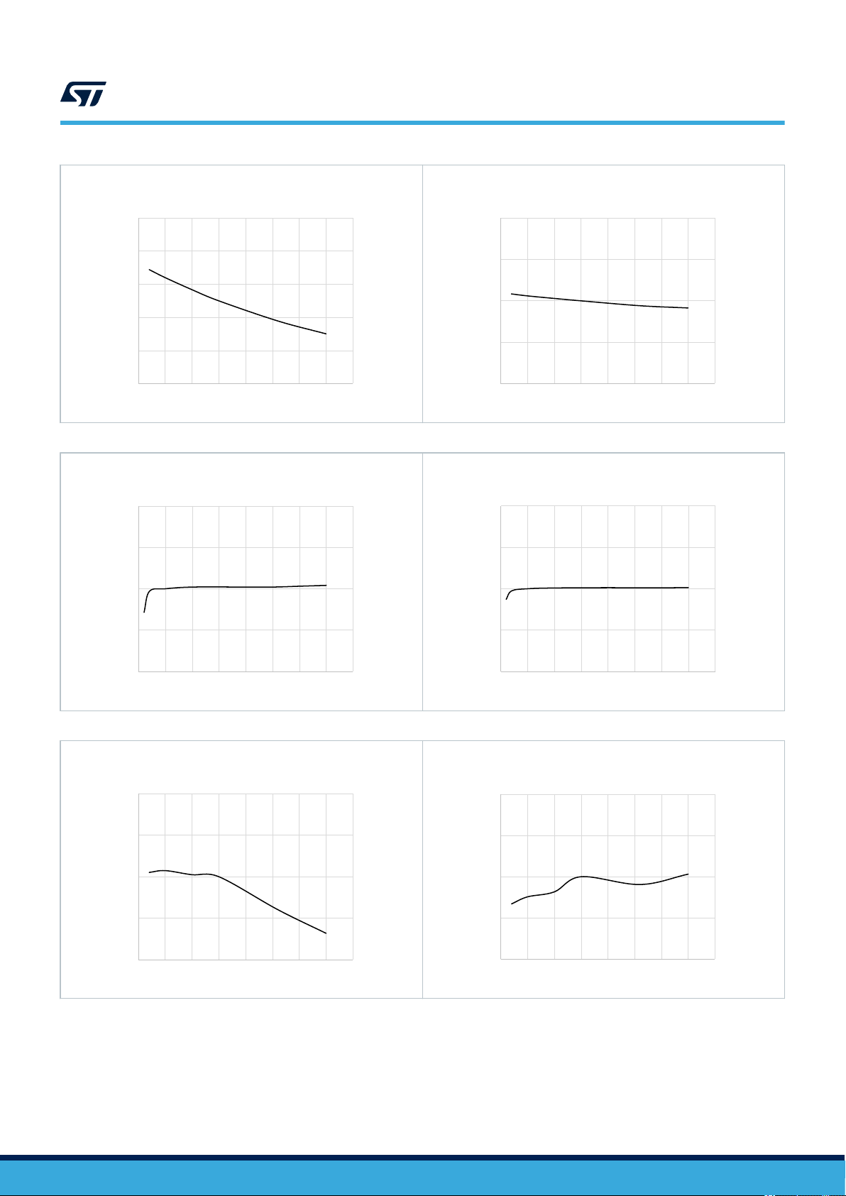
3 Typical electrical characteristics
0.8
0.9
1
1.1
1.2
-50 -25 0 25 50 75 100 125 150
I
DLIM
/(I
DLIM
@25°C)
Tj[°C]
0.9
0.95
1
1.05
1.1
-50 -25 0 25 50 75 100 125 150
F
OSC
/(F
OSC
@25°C)
Tj[°C]
0.8
0.9
1
1.1
1.2
-50 -25 0 25 50 75 100 125 150
V
HV_START
/(V
HV_START
@25°C)
Tj[°C]
0.95
0.975
1
1.025
1.05
-50 -25 0 25 50 75 100 125 150
V
FB_REF
/(V
FB_REF
@25°C)
Tj[°C]
0.9
0.95
1
1.05
1.1
-50 -25 0 25 50 75 100 125 150
Iq/(Iq@25°C)
Tj[°C]
0.8
0.9
1
1.1
1.2
-50 -25 0 25 50 75 100 125 150
ICC/(ICC@25°C)
Tj[°C]
VIPER31
Typical electrical characteristics
Figure 3. I
Figure 5. V
vs. T
DLIM
HV_START
J
vs. T
Figure 4. F
J
Figure 6. VF
OSC
B_REF
vs. T
vs. T
J
J
Figure 7. Quiescent Current Iq vs. T
DS13285 - Rev 2
J
Figure 8. Operating current ICC vs. T
J
page 9/40
Page 10
0.5
0.7
0.9
1.1
1.3
1.5
-50 -25 0 25 50 75 100 125 150
I
CH1
/(I
CH1
@25°C)
Tj[°C]
0.8
0.9
1
1.1
1.2
-50 -25 0 25 50 75 100 125 150
I
CH2
/(I
CH2
@25°C)
Tj[°C]
0.9
0.95
1
1.05
1.1
0 100 200 300 400 500 600 700 800
I
CH1
/(I
CH1@VDRAIN
= 100V)
V
DRAIN
[V]
0.9
0.95
1
1.05
1.1
0 100 200 300 400 500 600 700 800
I
CH2
/(I
CH2@VDRAIN
=100V)
V
DRAIN
[V]
0.8
0.9
1
1.1
1.2
-50 -25 0 25 50 75 100 125 150
GM/(GM@25°C)
Tj[°C]
0.9
0.95
1
1.05
1.1
-50 -25 0 25 50 75 100 125 150
I
COMP
/(I
COMP
@25°C)
Tj[°C]
VIPER31
Typical electrical characteristics
Figure 9. I
Figure 11. I
CH1
CH1
vs. V
vs. T
J
DRAIN
Figure 10. I
Figure 12. I
CH2
CH2
vs. T
vs. V
J
DRAIN
Figure 13. GM vs. T
DS13285 - Rev 2
J
Figure 14. I
COMP
vs. T
J
page 10/40
Page 11

0.00
0.50
1.00
1.50
2.00
2.50
-50 -25 0 25 50 75 100 125 150
Tj[°C]
R
DS(on)
/(R
DS(on)
@25°C)
0
0.5
1
1.5
0 50 100 150 200 250 300 350 400
I
[mA]
R
DS(on)
/(R
DS(on)@IDRAIN
= 360mA)
T = 25°C
1
10
100
1000
10000
0 1 10 100 1000
VDS[V]
C
OSS
[pF]
0.88
0.92
0.96
1
1.04
1.08
1.12
-50 0 50 100 150
TJ[°C]
V
(BR)DSS
/ (V
(BR)DSS
@ 250C)
ID= 1 mA
0.0
0.4
0.8
1.2
1.6
2.0
2.4
2.8
3.2
3.6
4.0
4.4
4.8
0.0 4.0 8.0 12.0 16.0 20.0
VDS[V]
I
DRAIN
[A]
-40°C
25°C
125°C
VIPER31
Typical electrical characteristics
Figure 15. R
DSON
vs. T
J
Figure 17. Static drain-source on resistance
Figure 16. R
Figure 18. Power MOSFET C
vs. I
DSON
OSS
DRAIN
vs. VDS @ VGS=0, f=1MHz
Figure 19. V
DS13285 - Rev 2
BVDSS
vs. T
J
Figure 20. Output characteristic
page 11/40
Page 12
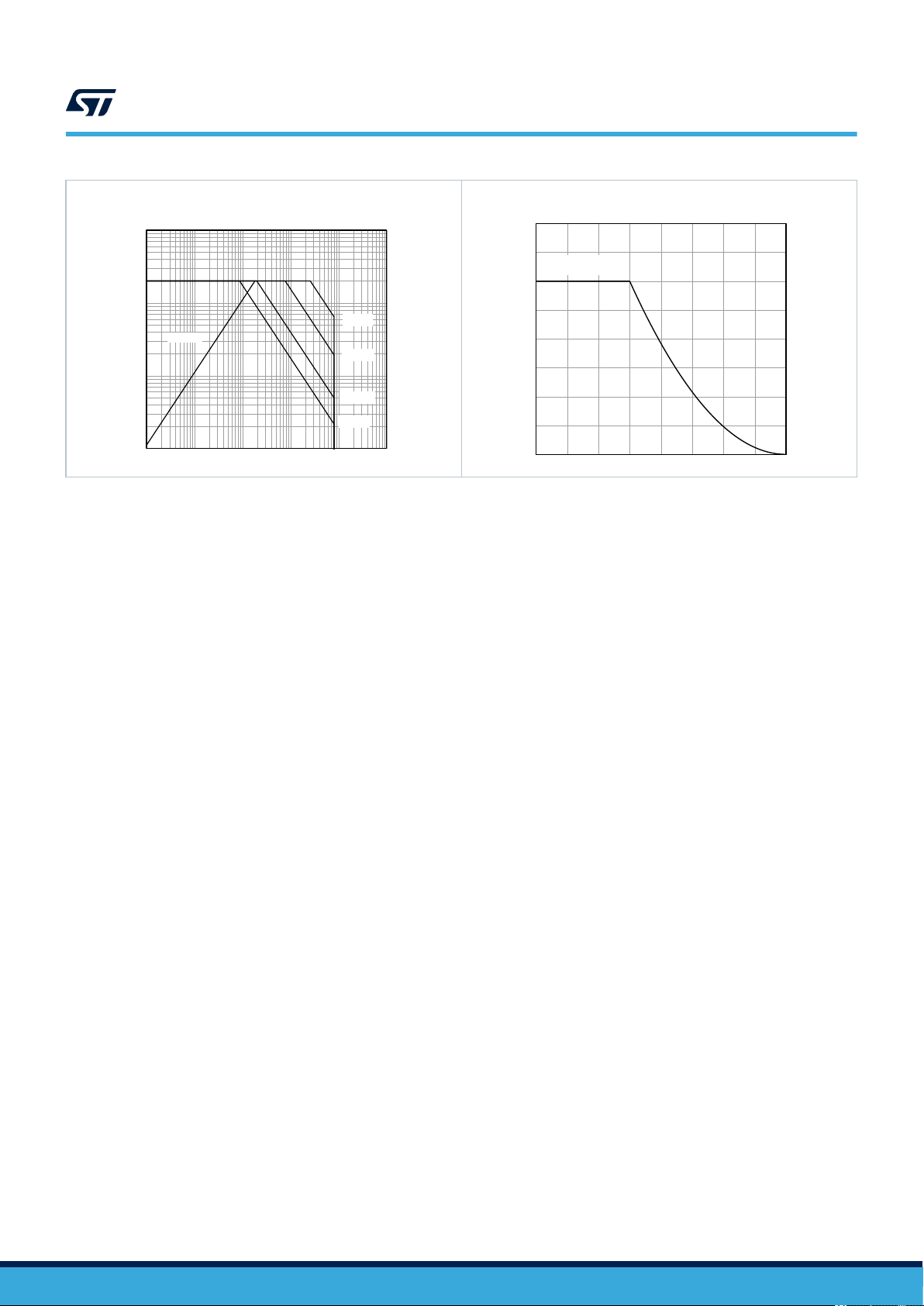
0.01
0.1
1
10
0.1 1 10 100 1000 10000
VDS[V]
ID[A]
tp= 1 ms
tp= 10 ms
tp= 1 ms
R
DS(on)
limit
tp= 100 ms
0
1
2
3
4
-50 0 50 100 150
Tj[°C]
EAS[mJ]
Single pulse,
ID= 1A, VDD= 50 V
VIPER31
Typical electrical characteristics
Figure 21. SOA SO16N package
Figure 22. Maximum avalanche energy vs. Tj
DS13285 - Rev 2
page 12/40
Page 13

4 General description
VCC DRAIN
Internal Supply bus
RSENSE
REGULATOR
4V
HV
Start up
THERMAL
DIODE
(OTP)
GND
HV DISABLE
LOGIC
SOFT START
JITTERED
OSCILLATOR
E/A
+
-
+
-
FB
V
FB_REF
PWM
-
+
TURN ON
LOGIC
COMP
OCP
UVLO VCC
VCC_clamp
t
OVL
filter
LEB
S
R
Q
OTP
OCP
-
+
I
DLIM
ref
LIGHT LOAD PFM
PROTECTION
LOGIC
t
RESTART
OVP LOGIC
t
OVP_REST
OVP
TSDLOGIC
t
RESTART
R
G
V
z
I
HV
I
CH*
+
-
-
V
OVP_th
+
-
+
-
V
UVP_th
t
OVP_DEB
filter
UVP
S
R
Q
IC DISABLE
LOGIC
IC_DIS
IC_DIS
t
UVP_REST
filter
IC_DIS_SET
IC_DIS_RESET
t
UVP_DEB
filter
+
4.1 Block diagram
VIPER31
General description
Figure 23. Block diagram
4.2 Typical power capability
Vin: 230 V
(1)
Adapter
27 W 31 W 16 W 19 W
1. Typical continuous power in non-ventilated enclosed adapter measured at 50°C ambient.
2. Maximum practical continuous power in an open frame design at 50°C ambient, with adequate heat sinking.
AC
Open Frame
Table 8. Typical power
(2)
Adapter
Vin: 85-265 V
(1)
AC
Open Frame
(2)
DS13285 - Rev 2
page 13/40
Page 14

VIPER31
Primary MOSFET
Figure 24. Typical deliverable output power vs. T
4.3 Primary MOSFET
(Vin: 85-265VAC)
AMB
The primary switch is implemented with an avalanche rugged N-channel MOSFET with 800 V minimum
breakdown voltage, V
BVDSS
The sense-FET is embedded and allows a virtually lossless current sensing.
The MOSFET gate driver controls the gate current during both turn-on and turn-off in order to minimize common
mode EMI. Under UVLO conditions the embedded pull-down circuit holds the gate low in order to ensure that the
MOSFET cannot be turned on accidentally.
4.4 High-voltage startup
The embedded high-voltage startup includes both the 800 V startup FET, whose gate is biased through the
resistor RG, and the switchable HV current source, delivering the current IHV. The major portion of IHV, (ICH),
charges the capacitor connected to VCC pin. A minor portion is sunk by the controller block.
Power on: at startup, as the voltage across the DRAIN pin exceeds the V
source is turned on, charging linearly the VCC capacitor with the current I
is reduced to I
case the pin is accidentally shorted to GND.
As VCC reaches the startup threshold, V
the HV current source is disabled and the device is powered by the energy stored in the VCC capacitor. The IC
can be supplied through a transformer auxiliary winding or, in case of not isolated topologies with V
directly from the converter’s output.
The supply operating range is from 4.5 V to 30.5 V. If VCC pin voltage exceeds 30.5 V (referred to V
internal clamp could be reached, which causes the VIPER31 to stop switching.
This condition is potentially dangerous for the VIPER31 and must be avoided, by means of proper transformer
design and/or external protection (zener diode between VCC and GND pins).
In normal operation the HV current source is always kept off by maintaining VCC above V
consumption is given by the power dissipated on RG only, calculated as follows:
(1 mA typ.) in case VCC is lower than 1 V (typical value), in order to limit IC power dissipation in
CH1
, and 3.5 Ω maximum on-resistance, R
, the chip starts operating, the primary MOSFET is enabled to switch,
CCon
DS(on)
.
HV_START
CH2
threshold, the HV current
(8.8 mA typ.). This charging current
OUT
GND
, so its residual
Cson
≥ 5 V,
), the
DS13285 - Rev 2
Equation 1
PHV(VIN) = V
(1)
2
/R
IN
G
page 14/40
Page 15

V
IN_DC
Power-off:
VINdecreases
V
DRAIN
Power-on:
HV current source enabled
t
V
CCon
1V
I
CH1
I
CH2
V
CSon
V
CCoff
HV current source is no
more activated because
of too low V
DRAIN
UVLO
V
CC
HV current source is
disabled here
V
OUT
Output regulation is lost here
V
HV_START
t
t
t
Power-on
Power-off
Steady-state
VIPER31
Soft startup
At nominal input voltage (230 VAC), typical and worst-case consumptions are 2.4 mW and 3.0 mW respectively
(corresponding to RG_typ = 45 Mohm and RG_min = 36 Mohm). This means that, with a careful design, the
overall no-load input power consumption of the application can be maintained very low (typically, below 10 mW
@230 VAC)
Power-off: when the IC is disconnected from the mains, or there is a mains interruption, for some time the
converter keeps on working, powered by the energy stored in the input bulk capacitor. When it is discharged
below a critical value, the converter is no longer able to keep the output voltage regulated. During the power
down, when the DRAIN voltage becomes too low, the HV current source remains off and the IC is stopped as
soon as VCC drops below the UVLO threshold, V
Figure 25. Power ON and power OFF
Ccoff
.
4.5
Soft startup
The internal soft-start function of the VIPer31 progressively increases the cycle-by-cycle current limitation set
point from zero up to I
The soft-start time, tSS, which is internally set at 8 ms, is activated at any attempt of converter power-on and at
any restart after a fault event.
DS13285 - Rev 2
The feature is used to reduce the stress of the power components and increase the reliability of the system.
DLIM
.
page 15/40
Page 16

Figure 26. Soft startup
Soft start phase
Steady state
time
time
I
DLIM
t
SS
I
DRAIN
V
OUT
time
V
COMP
V
COMPH
V
OUT
VIPER31
Oscillator
4.6 Oscillator
The IC embeds a fixed frequency oscillator with jittering feature. The switching frequency is modulated by
approximately ±7%·F
distributes the energy of each harmonic of the switching frequency over a number of frequency bands, having the
same energy on the whole but smaller amplitudes. This helps to reduce the conducted emissions, especially
when measured with the average detection method or, which is the same, to pass the EMI tests with an input filter
of smaller size with respect to the one that should be needed in absence of jittering feature. Three switching
frequency options, F
4.7 Pulse skipping
The IC embeds a pulse skip circuit that operates in the following way:
• Each time the DRAIN peak current exceeds I
The cycles can be skipped until the minimum switching frequency F
• Each time the DRAIN peak current does not exceed I
restored. The cycles can be restored until the nominal switching frequency FOSC is reached.
The protection is intended in order to avoid the so called “flux runaway” condition often present at converter
startup and due to the fact that the primary MOSFET, which is turned on by the internal oscillator, cannot be
turned off before the minimum on-time.
During the on-time, the inductor is charged through the input voltage and, if it cannot be discharged by the same
amount during the off-time, in every switching cycle there is a net increase of the average inductor current, that
can reach dangerously high values until the output capacitor is not charged enough to ensure the inductor
discharge rate needed for the volt-second balance. This condition is common at converter startup, because of the
low output voltage.
In the following Figure 27. Pulse skipping during startup the effect of pulse skipping feature on the DRAIN peak
current shape is shown (solid line), compared with the DRAIN peak current shape when pulse skipping feature is
not implemented (dashed line). Providing more time for cycle-by-cycle inductor discharge when needed, this
feature is effective in keeping low the maximum DRAIN peak current avoiding the flux runaway condition.
at 200 Hz rate. The purpose of the jittering is to get a spread-spectrum action that
OSC
, are available: 30 kHz (X type), 60 kHz (L type) and 132 kHz (H type).
OSC
level within t
DLIM
DLIM
within t
, the next switching cycle is skipped.
ON_MIN
OSC_MIN
ON_MIN
(15 kHz) is reached.
, the next switching cycle is
DS13285 - Rev 2
page 16/40
Page 17

Figure 27. Pulse skipping during startup
time
V
OUT
DRAIN
time
I
DLIM
with pulse skipping
without pulse skipping
skipped cycles
V
OUT_nom
VIPER31
Direct feedback
4.8 Direct feedback
The IC embeds a transconductance type error amplifier (E/A) whose inverting input and output are FB and COMP,
respectively. The internal reference voltage of the E/A is V
isolated topologies, a positive output voltage can be tightly set through a simple voltage divider applied among the
output voltage terminal, FB and GND.
The E/A output is scaled down and fed into the PWM comparator, where it is compared to the voltage across the
sense resistor in series to the sense-FET, thus setting the cycle-by-cycle drain current limitation.
An R-C network connected on the output of the error amplifier (COMP) is usually used to stabilize the overall
control loop.
The FB is provided with an internal pull-up to prevent a wrong IC behavior when the pin is accidentally left
floating.
The E/A is disabled if the FB voltage is lower than V
4.9 Secondary feedback
When a secondary feedback is required, the internal E/A has to be disabled shorting FB to GND (VFB < V
With this setting, COMP is internally connected to the parallel of a 100 uA current generator and the 15 kΩ (typ.)
4.10
R
COMP(DYN)
This allows to set the output voltage value through an external error amplifier (TS431 or similar) placed on the
secondary side, whose error signal is used to set the DRAIN peak current setpoint corresponding to the output
power demand. If isolation is required, the error signal must be transferred through an optocoupler, with the
phototransistor collector connected across COMP and GND.
Pulse frequency modulation
resistor, and the voltage across COMP is set by the current sunk.
FB_REF
(200 mV, typ).
FB_DIS
(1.2 V typical value referred to GND). In non-
FB_DIS
).
DS13285 - Rev 2
If the output load is decreased, the feedback loop reacts by lowering V
current setpoint. The minimum value is I
If the load is further decreased, the DRAIN peak current value is maintained at I
are skipped. This kind of operation is referred to as “pulse frequency modulation” (PFM), the number of the
DLIM_PFM
, corresponding to the V
which reduces the DRAIN peak
COMP,
threshold.
COMPL
DLIM_PFM
and some PWM cycles
skipped cycles depending on the balance between the output power demand and the power transferred from the
input. The result is an equivalent switching frequency which can go down to some hundreds Hz, thus reducing all
the frequency-related losses.
page 17/40
Page 18

This kind of operation, together with the extremely low IC quiescent current, allows very low input power
time
V
CC
V
CCon
V
CSon
DRAIN
I
DLIM
t
OVL
t
RESTART
t
SS
t
OVL
Overload applied
t
SS
time
Overload removed
t
RESTART
consumption in no-load and light load, while the low DRAIN peak current value, I
noise which could arise from low switching frequency values. When the output load is increased, V
increases and PFM is exited. V
limitation (IDLIM).
4.11 Overload protection
In order to manage the overload condition the IC embeds the following main blocks: the OCP comparator to turn
off the power MOSFET when the drain current reaches its limit (I
the turn-off delay time in case of continuous overload (t
after protection tripping (t
In case of short-circuit or overload, the control level on the inverting input of the PWM comparator is greater than
the reference level fed into the inverting input of the OCP comparator. As a result, the cycle-by-cycle turn off of
the power switch is triggered by the OCP comparator instead of by the PWM comparator. Every cycle this
condition is met, the OCP counter is incremented. If the fault condition persists for a time greater than t
(corresponding to the counter end-of-count), the protection is tripped, the PWM is disabled for t
resumes switching with soft-start and, if the fault is still present, it is disabled again after t
management prevents the IC from being indefinitely operated at I
attempts of the converter avoids overheating the IC in case of repeated fault events.
After the fault removal, the IC resumes working normally. If the fault is removed before the protection tripping
(before t
OVL
), the t
tripped. If the fault is removed during t
resuming switching.
In fault condition, VCC is kept between V
which recharges the VCC capacitor to V
RESTART
counter is decremented on a cycle-by-cycle basis down to zero and the protection is not
OVL
reaches its maximum at V
COMP
= 1 sec, typ.).
RESTART
, the IC waits for the t
and V
CSon
any time the IC internal consumption discharges it to V
Ccon
Overload protection
DLIM_PFM
, corresponding to the DRAIN current
COMPH
), the up and down OCP counter to define
DLIM
= 50 ms typ.) and the timer to define the restart time
OVL
and the low repetition rate of the restart
DLIM
RESTART
by the periodical activation of the HV current source,
CCon
period ot have elapsed before
, prevents any audible
RESTART
. The OLP
OVL
VIPER31
COMP
OVL
, then it
.
Cson
Figure 28. Overload protection
4.12 Undervoltage protection
If the voltage across the UVP pin (V
than t
UVP_DEB
When V
Both t
UVP_DEB
(30 ms, typ.), the IC is disabled and its consumption is reduced to ultra-low values (I
rises above V
UVP
and t
UVP_th
UVP_REST
are intended to filter out possible noises/disturbances of the line, which could affect
the correct operation of the function. They are obtained through two separate up/down counters:
DEB (REST) up/down counter has a deb_eoc (rest_eoc) end-of-count. The operation is illustrated in
Figure 29. UVP timing.
If the counter starts from zero and counts always up, end-of-count is reached in a time interval t
(t
UVP_REST
).
) falls below the internal threshold V
UVP
, the IC must wait t
UVP_REST
(0.4 V typ.) for a time greater
UVP_th
q_DIS
(30 ms, typ.) before resuming switching.
UVP_DEB
).
DS13285 - Rev 2
page 18/40
Page 19

V
UVP
I
DRAIN
rest_eoc
V
UVP
_th
V
DD
IC re-enabled
IC disabled
normal operation
disabled with ultra-low consumption (I
q_DIS
)
normal operation
t
UVP_REST
Restart
delay
V
CCon
V
CSon
DEB counter
t
UVP_DEB
< t
UVP_DEB
deb_eoc
VIPER31
Undervoltage protection
If V
falls below V
UVP
reached, the counter is decremented. If the count goes back down to zero, a disturbance on the UVP pin is
assumed and there is no consequence on the IC behavior.
If V
stays below V
UVP
are turned off and the internal consumption is reduced to I
the periodical activation of the internal HV-current source; the DEB counter is reset. Of course, if during the count-
up V
exceeds V
UVP
delayed accordingly.
With IC disabled: if V
(corresponding to t
V
for some time, the REST counter is decremented during that time and the IC re-enabling is delayed
UVP_th
UVP_REST
accordingly.
, the DEB counter is incremented. If V
UVP_th
until the counter reaches deb_eoc: the device is disabled; most of the internal blocks
UVP_th
q_DIS
for some time, the DEB counter is decremented during that time and the IC disable is
UVP_th
rises above V
UVP
, the REST counter is incremented, and when it reaches rest_eoc
UVP_th
), the IC resumes switching. Of course, if during the count-up, V
increases above V
UVP
_th before uvp_eoc is
UVP
; VCC is maintained between V
Cson
UVP
Figure 29. UVP timing
and V
Ccon
falls below
by
DS13285 - Rev 2
An input undervoltage protection can be easily realized connecting the rectified mains to UVP pin through a
voltage divider, as shown in Figure 30. Connection for input undervoltage protection/disable (isolated or non-
isolated topologies).
page 19/40
Page 20

C1
Cs
GND
DRAIN
GND
VCC
UVPCOMP
CONTROL
FB
VIPER31
RH
D
IN
RL
~ AC
OVP
C
IN
from V
AUX
or V
OUT
C2
R2
VIPER31
Undervoltage protection
Figure 30. Connection for input undervoltage protection/disable (isolated or non-isolated topologies)
If UVP function is not required, the UVP pin must be left floating. In this case, noise immunity of the pin is
guaranteed by the internal pull-up I
UVP_pull-up
(1 uA, typ.) present in the UVP block.
If UVP function is required, RH value can be set arbitrarily, but some Mohms at least are recommended in order to
minimize the power consumption of the UVP network. Then, if V
is the desired input undervoltage threshold,
in_UVP
the value of RL can be found from the following formula:
Equation 2
(2)
V
RL =
V
in_UVP
− V
RH
UVP_th
UVP_th
+ I
UVP_pull − up
Equation 3
(3)
2
PUVP Vin =
Vin
RH + RL
Thanks to the ultra-low consumption, the UVP pin can be used as an input to disable the SMPS from external,
reaching the lowest input power consumption while the SMPS is still connected to the AC mains but not delivering
power to its output.
The purpose of the UVP debounce time t
the input line, as illustrated in Figure 31. Hold-up in case of input line missing cycles.
UVP_DEB
is also to guarantee some hold-up in case of a missing cycle of
DS13285 - Rev 2
page 20/40
Page 21

Figure 31. Hold-up in case of input line missing cycles
UVP_th
1 missing cycle
V
BULK
t
UVP_DEB
V
UVP
t
UVP_DEB
2 missing cycles
I
DRAIN
IC disabled
here
4.13 Overvoltage protection
VIPER31
Overvoltage protection
If the voltage across OVP pin (V
t
OVP_DEB
below V
The time interval t
(250 us, typ.), the PWM is disabled in autorestart for t
.
OVP_th
OVP_DEB
is intended to filter out possible noises/disturbances of the line, which could affect the
correct operation of the function, and is obtained through an up/down counter, where t
) exceeds the internal threshold V
OVP
OVP_th
OVP_REST
(4 V typ.) for a time greater than
time (500 ms, typ.), until V
OVP_DEB
is the time the
OVP
falls
counter needs to reach its end-of-count (ovp_eoc) starting from zero and counting always up.
The operation is shown in Figure 32. OVP timing. When V
exceeds V
OVP
, the up/down OVP counter is
OVP_th
incremented.
If V
falls below V
OVP
before the OVP counter reaches ovp_eoc, the counter is decremented. If the count
OVP_th
goes down to zero, a disturbance on the OVP pin is assumed and there is no consequence on the IC behavior.
If V
t
activation of the internal HV-current source. Of course, if during the count-up V
stays above V
OVP
OVP_REST
until the OVP counter reaches ovp_eoc: the PWM is disabled in autorestart for a
OVP_th
time interval; the OVP counter is reset; VCC is maintained between V
and V
Cson
falls below V
OVP
by the periodical
Ccon
OVP_th
for some
time, during that time the counter is decremented and the PWM disable is delayed accordingly.
When V
drops below V
OVP
, the IC waits for the end of t
OVP_th
OVP_REST
, then restarts with soft-start phase.
DS13285 - Rev 2
page 21/40
Page 22

Figure 32. OVP timing
V
OVP
OVP count
GD
OVP triggered
and IC disabled
V
OVP
_th
V
DD
OVP check and
IC re-enabled
OVP check and
IC disabled
< t
OVP_DEB
t
OVP_DEB
t
OVP_REST
t
OVP_REST
t
OVP_DEB
V
CCon
V
CSon
VIPER31
Overvoltage protection
An input overvoltage protection can be easily realized connecting the rectified mains to OVP pin through a voltage
divider, as shown in Figure 33. Connection for input overvoltage protection (iso/non-iso topologies).
In case of non-isolated topologies, with the same principle an output overvoltage protection can be implemented,
as shown in Figure 34. Connection for output overvoltage protection (non-iso topologies).
If the OVP feature is not required, OVP pin must be connected to GND, which excludes the function.
If the OVP feature is required, RH value can be set arbitrarily, but some Mohms at least are recommended in
order to minimize the power consumption of the OVP network. Then, if V
in/out_OVP
is the desired input/output
overvoltage threshold, the value of RL can be calculated from the following formula:
Equation 4
(4)
RL =
The power consumption of the OVP network at given Vin is expressed as:
Equation 5
RH
V
in/out_ OVP
V
OVP_tℎ
− 1
(5)
2
POVP Vin =
Vin
RH + RL
in case of connection for input overvoltage protection and
Equation 6
POVP VOUT =
VOUT
RH + RL
2
(6)
DS13285 - Rev 2
in case of connection for output overvoltage protection.
page 22/40
Page 23

C1
Cs
GND
DRAIN
GND
VCC
UVPCOMP
CONTROL
FB
VIPER31
RH
D
IN
RL
~ AC
OVP
C
IN
from V
AUX
or V
OUT
C2
R2
C1
Cs
D
OUT
GND
RH
RLRfb2
Rfb1
DRAIN
GND
VCC
UVPCOMP
CONTROL
FB
VIPER31
OVP
C
OUT
V
OUT
from V
AUX
or V
OUT
C2
R2
Undervoltage and overvoltage protection
Figure 33. Connection for input overvoltage protection (iso/non-iso topologies)
VIPER31
Figure 34. Connection for output overvoltage protection (non-iso topologies)
4.14
Undervoltage and overvoltage protection
If both undervoltage and overvoltage protections are required, they can be set independently from each other
through a single voltage divider, as illustrated in the figure below.
DS13285 - Rev 2
page 23/40
Page 24

C1
Cs
GND
DRAIN
GND
VCC
UVPCOMP
CONTROL
FB
VIPER31
C
IN
RH
D
IN
RL
~ AC
OVP
RM
from V
AUX
or V
OUT
C2
R2
VIPER31
Undervoltage and overvoltage protection
Figure 35. Connection for input and output overvoltage protections (iso/non-iso topologies)
The voltage divider equations are:
Equation 7
(7)
V
UVP
tℎ
V
in_UVP
=
RL
− I
UVP_pull − up
· RH + RM + RL + RL · I
UVP_pull − up
Equation 8
(8)
V
in_OVP
= V
OVP
−
tℎ
RH + RM + RL
RH
·
RL · I
UVP_pull − up
RH + RM + RL
·
RM + RL
Considering that the value of RH is much higher than the values of RM and RL (Mohms vs. kohms), equations 7
and 8 can be approximated into Eq. 7.a) and Eq. 8.a) respectively:
Equation 7.a
(7.a)
V
UVP
tℎ
V
in_UVP
RL
− I
UVP_pull − up
· RH + RL · I
UVP_pull − up
Equation 8.a
V
in_OVP
V
OVP
− RL · I
tℎ
Selecting arbitrarily the RH value, Equation 7.a) can be solved for RL:
Equation 9
RL =
V
in_UVP
+ I
UVP_pull − up
UVP_pull − up
· RH − V
·
RM + RL
in_UVP
RH
+ I
UVP_pull − up
2 · I
UVP_pull − up
· RH2− 4 · V
UVP
· I
UVP_pull − up
tℎ
· RH
(8.a)
(9)
and Equation 8.a) for RM:
DS13285 - Rev 2
page 24/40
Page 25

Equation 10
V
CCon
GD
t
V
CC
V
CSon
t
RESTART
T
J
n < n
th
T
SD
t
RESTART
t
t
n = n
th
n = n
th
RM = V
OVP
− RL · I
tℎ
UVP_pull − up
·
V
RH
in_OVP
− RL
The power consumption of the UVP-OVP network at given Vin is expressed as:
Equation 11
2
V
P
UVP_OVPVin
=
in
RH + RM + RL
VIPER31
Thermal shutdown
(10)
(11)
As an example, if V
in_UVP
Mohm: from Equations 9 and 10 we have RL = 43 kohm, and RM = 60 kohm respectively, while from Equation 11
the power consumption of the network at 230 Vac is about 17 mW.
4.15 Thermal shutdown
The power MOSFET junction temperature is sensed during the on-time through a diode integrated into the HV
section of the chip. If a junction temperature higher than the internal threshold TSD (160°C, typ.) is measured, the
PWM is disabled for t
triggered only if the condition is met for nth = 3 consecutive switching cycles.
After t
RESTART
measured for nth consecutive switching cycles, the protection is triggered and PWM is disabled again for
t
RESTART
During t
; otherwise normal operation is restored.
RESTART
Such a behavior is summarized in Figure 36. Thermal shutdown timing diagram.
RESTART
, the IC resumes switching with soft-start phase: if a junction temperature above TSD is still
, V
is maintained between V
CC
and V
design values are 50 Vdc and 450 Vdc respectively, and RH is set to 6
in_OVP
. In order to increase robustness against electromagnetic noises, the protection is
Cson
and V
by the HV current source periodical activation.
Ccon
Figure 36. Thermal shutdown timing diagram
DS13285 - Rev 2
page 25/40
Page 26

5 Application information
Vout
GND
C1
Din
Rcl
C2
Cout
Cin
Rin
R2
Daux
Cs
RH
T
Dout
RL
CONTROL
OVP
DRAIN
GND
VCC
FB
COMP UVP
VIPER31
Ccl
Vout
GND2
DRAIN
GND
VCC
UVPCOMP
CONTROL
FB
OVP
VIPER31
RH
Dout
R3
C2
Rin
OPTO
C1
Rcl
Ccl
Raux
Daux
OPTO
Cs
Cout
T
R4
RL
Cin
Din
5.1 Typical schematics
Figure 37. Flyback converter (non-isolated)
VIPER31
Application information
Figure 38. Flyback converter (isolated)
DS13285 - Rev 2
page 26/40
Page 27

Figure 39. Flyback converter (primary regulation)
Vout
GND2
Cin
RH
Din
C2
Rcl
T
C1
RL
DRAIN
GND
VCC
UVPCOMP
CONTROL
FB
OVP
VIPER31
Ccl
Cout
Cs
Daux
Rin
Dout
R2
Vout
~ AC
Lout
DRAIN
GND
VCC
UVPCOMP
CONTROL
FB
OVP
VIPER31
RL
C3
Daux
Din
Cout
Cin
RH
Rin
D2
D1
C1
R2CsC2
Vout
GNDGND
Din
C3
DRAIN
GND
VCC
UVPCOMP
CONTROL
FB
OVP
VIPER31
C1
Cin
Rin
R2
Daux
D2
Lout
C2
RH
D1
Cs
RL
Cout
Figure 40. Buck converter
VIPER31
Typical schematics
DS13285 - Rev 2
Figure 41. Buck-boost converter
page 27/40
Page 28

5.2 Energy saving performances
10
20
30
40
50 100 150 200 250 300
P
IN
[mW]
VIN[VAC]
The VIPer31 allows the design of applications compliant with the most stringent energy saving regulations. In
order to show the typical performances achievable, the active mode average efficiency and the efficiency at 10%
of the rated output power of a single output flyback converter using VIPer31 have been measured and are
reported in Table 9. In addition, Figures 52 and 53 show no-load and light load consumptions.
Table 9. Power supply efficiency, VOUT = 15 V
VIPER31
Energy saving performances
Parameter
Flyback iso, 15V/1.2A
V
IN
115 V
AC
230 V
AC
Figure 42. PIN versus VIN in no-load, VOUT = 15V
10% output load
efficiency [%]
83.2 85.9 26.0
77.4 86.6 29.7
Active mode average
efficiency [%]
Pin @ no-load
[mW]
DS13285 - Rev 2
page 28/40
Page 29

Figure 43. PIN versus VIN in light-load, VOUT = 15V
0
50
100
150
200
250
300
350
400
450
50 100 150 200 250 300
P
IN
[mW]
VIN[VAC]
P
OUT
= 25mW
P
OUT
= 50mW
P
OUT
= 250mW
VIPER31
Energy saving performances
DS13285 - Rev 2
page 29/40
Page 30

Layout guidelines and design recommendations
5.3 Layout guidelines and design recommendations
A proper printed circuit board layout is essential for correct operation of any switch-mode converter and this is
true for the VIPer as well. The main reasons to have a proper PCB layout are to:
• Provide clean signals to the IC, ensuring good immunity against external noises and switching noises
• Reduce the electromagnetic interferences, both radiated and conducted, to pass more easily the EMC
When designing an SMPS using VIPer, the following basic rules should be considered:
• Separating signal from power tracks: generally, traces carrying signal currents should run far from those
carrying pulsed currents or with quickly swinging voltages. Signal ground traces should be connected to the
IC signal ground, GND, using a single “star point”, placed close to the IC. Power ground traces should be
connected to the IC power ground, GND. The compensation network should be connected to the COMP,
maintaining the trace to GND as short as possible. In case of two layer PCB, it is a good practice to route
signal traces on one PCB side and power traces on the other side.
• Filtering sensitive pins: some crucial points of the circuit need or may need filtering. A small high-
frequency bypass capacitor to GND might be useful to get a clean bias voltage for the signal part of the IC
and protect the IC itself during EFT/ESD tests. A low ESL ceramic capacitor (a few hundreds pF up to 0.1
μF) should be connected across VCC and GND, placed as close as possible to the IC. With flyback
topologies, when the auxiliary winding is used, it is suggested to connect the VCC capacitor on the auxiliary
return and then to the main GND using a single track.
• Keep power loops as confined as possible: minimize the area circumscribed by current loops where high
pulsed currents flow, in order to reduce its parasitic self-inductance and the radiated electromagnetic field:
this greatly reduces the electromagnetic interferences produced by the power supply during the switching. In
a flyback converter the most critical loops are: the one including the input bulk capacitor, the power switch,
the power transformer, the one including the snubber, the one including the secondary winding, the output
rectifier and the output capacitor. In a buck converter the most critical loop is the one including the input bulk
capacitor, the power switch, the power inductor, the output capacitor and the free-wheeling diode.
• Reduce line lengths: any wire acts as an antenna. With the very short rise times exhibited by EFT pulses,
any antenna has the capability of receiving high-voltage spikes. By reducing line lengths, the level of
radiated energy that is received is reduced, and the resulting spikes from electrostatic discharges are lower.
This also keeps both resistive and inductive effects to a minimum. In particular, all of the traces carrying high
currents, especially if pulsed (tracks of the power loops) should be as short and fat as possible.
• Optimize track routing: as levels of pickup from static discharges are likely to be greater closer to the
extremities of the board, it is wise to keep any sensitive lines away from these areas. Input and output lines
often need to reach the PCB edge at some stage, but they can be routed away from the edge as soon as
possible where applicable. Since vias are to be considered inductive elements, it is recommended to
minimize their number in the signal path and avoid them when designing the power path.
• Improve thermal dissipation: an adequate copper area has to be provided under the DRAIN pins as heat
sink, while it is not recommended to place large copper areas on the GND.
VIPER31
DS13285 - Rev 2
page 30/40
Page 31

C1
OPTO
R
OPTO
~ AC
D
IN
Cs
OPTO
RL
RH
TR
C
OUT
V
OUT
GROUND
D
OUT
CONTROL
DR.DR. DR. DR. N.C. N.C. N.C. N.C.
N.C.GND VCC N.A. UVP OVP FB COMP
VIPER31
R
C
R
IN
C
IN
C
CL
R
CL
D
AUX
C
C
C1
D1RL
RHCs
Cc
GROUND
CONTROL
DR.DR. DR. DR. N.C. N.C. N.C. N.C.
N.C.GND VCC N.A. UVP OVP FB COMP
VIPER31
~ AC
DINR
IN
C
IN
D
AUX
L
OUT
D
OUT
C
OUT
V
OUT
Layout guidelines and design recommendations
Figure 44. Recommended routing for flyback converter
VIPER31
Figure 45. Recommended routing for buck converter
DS13285 - Rev 2
page 31/40
Page 32

6 Package information
In order to meet environmental requirements, ST offers these devices in different grades of ECOPACK packages,
depending on their level of environmental compliance. ECOPACK specifications, grade definitions and product
status are available at: www.st.com. ECOPACK is an ST trademark.
6.1 SO16N package information
VIPER31
Package information
Figure 46. SO16N package outline
DS13285 - Rev 2
page 32/40
Page 33

Table 10. SO16N mechanical data
VIPER31
SO16N package information
Dim.
Min. Typ. Max.
A 1.75
A1 0.1 0.25
A2 1.25
b 0.31 0.51
c 0.17 0.25
D 9.8 9.9 10
E 5.8 6 6.2
E1 3.8 3.9 4
e 1.27
h 0.25 0.5
L 0.4 1.27
k 0 8
ccc 0.1
mm
DS13285 - Rev 2
page 33/40
Page 34

7 Order code
Order code
VIPER319XDTR 990 mA 30 kHz ± 7%
VIPER318HDTR 850 mA 132 kHz ± 7%
I
DLIM
Table 11. Order code
(OCP) typ
VIPER31
Order code
FOSC ± jitter Package
SO16N tape and reelVIPER318LDTR 850 mA 60 kHz ± 7%
DS13285 - Rev 2
page 34/40
Page 35

Revision history
Table 12. Document revision history
Date Version Changes
31-Mar-2020 1 Initial release.
8-Jun-2020 2
Updated Section Features; updated Table 6, Table 7, Table 11; updated
figures in Section 5.1 Typical schematics; minor text update.
VIPER31
DS13285 - Rev 2
page 35/40
Page 36

VIPER31
Contents
Contents
1 Pin setting.........................................................................2
2 Electrical and thermal ratings ......................................................4
2.1 Electrical characteristics .........................................................5
3 Typical electrical characteristics ...................................................9
4 General description...............................................................13
4.1 Block diagram ................................................................13
4.2 Typical power capability ........................................................13
4.3 Primary MOSFET .............................................................14
4.4 High-voltage startup ...........................................................14
4.5 Soft startup...................................................................15
4.6 Oscillator ....................................................................16
4.7 Pulse skipping ................................................................16
4.8 Direct feedback ..............................................................17
4.9 Secondary feedback ...........................................................17
4.10 Pulse frequency modulation.....................................................17
4.11 Overload protection ...........................................................18
4.12 Undervoltage protection ........................................................18
4.13 Overvoltage protection .........................................................21
4.14 Undervoltage and overvoltage protection .........................................23
4.15 Thermal shutdown.............................................................25
5 Application information ...........................................................26
5.1 Typical schematics ............................................................26
5.2 Energy saving performances ...................................................28
5.3 Layout guidelines and design recommendations ...................................30
6 Package information..............................................................32
6.1 [Package name] package information ............................................32
7 Order code .......................................................................34
Revision history .......................................................................35
Contents ..............................................................................36
DS13285 - Rev 2
page 36/40
Page 37

VIPER31
Contents
List of tables ..........................................................................38
List of figures..........................................................................39
DS13285 - Rev 2
page 37/40
Page 38

VIPER31
List of tables
List of tables
Table 1. Pin description......................................................................2
Table 2. Absolute maximum ratings ............................................................. 4
Table 3. Thermal data.......................................................................4
Table 4. Avalanche characteristics ..............................................................5
Table 5. Power section ......................................................................5
Table 6. Supply section......................................................................6
Table 7. Controller section.................................................................... 7
Table 8. Typical power .....................................................................13
Table 9. Power supply efficiency, VOUT = 15 V .................................................... 28
Table 10. SO16N mechanical data .............................................................. 33
Table 11. Order code ....................................................................... 34
Table 12. Document revision history............................................................. 35
DS13285 - Rev 2
page 38/40
Page 39

VIPER31
List of figures
List of figures
Figure 1. Connection diagram ................................................................2
Figure 2. R
Figure 3. I
Figure 4. F
Figure 5. V
Figure 6. VF
Figure 7. Quiescent Current Iq vs. TJ............................................................9
Figure 8. Operating current ICC vs. TJ...........................................................9
Figure 9. I
Figure 10. I
Figure 11. I
Figure 12. I
Figure 13. GM vs. TJ....................................................................... 10
Figure 14. I
Figure 15. R
Figure 16. R
Figure 17. Static drain-source on resistance ...................................................... 11
Figure 18. Power MOSFET C
Figure 19. V
Figure 20. Output characteristic ............................................................... 11
Figure 21. SOA SO16N package .............................................................. 12
Figure 22. Maximum avalanche energy vs. Tj ..................................................... 12
Figure 23. Block diagram ................................................................... 13
Figure 24. Typical deliverable output power vs. T
Figure 25. Power ON and power OFF ........................................................... 15
Figure 26. Soft startup ..................................................................... 16
Figure 27. Pulse skipping during startup .........................................................17
Figure 28. Overload protection................................................................ 18
Figure 29. UVP timing...................................................................... 19
Figure 30. Connection for input undervoltage protection/disable (isolated or non-isolated topologies) ............... 20
Figure 31. Hold-up in case of input line missing cycles ............................................... 21
Figure 32. OVP timing ..................................................................... 22
Figure 33. Connection for input overvoltage protection (iso/non-iso topologies) .............................. 23
Figure 34. Connection for output overvoltage protection (non-iso topologies) ................................23
Figure 35. Connection for input and output overvoltage protections (iso/non-iso topologies)...................... 24
Figure 36. Thermal shutdown timing diagram...................................................... 25
Figure 37. Flyback converter (non-isolated) .......................................................26
Figure 38. Flyback converter (isolated) .......................................................... 26
Figure 39. Flyback converter (primary regulation) ................................................... 27
Figure 40. Buck converter ...................................................................27
Figure 41. Buck-boost converter............................................................... 27
Figure 42. PIN versus VIN in no-load, VOUT = 15V .................................................28
Figure 43. PIN versus VIN in light-load, VOUT = 15V ................................................ 29
Figure 44. Recommended routing for flyback converter ............................................... 31
Figure 45. Recommended routing for buck converter ................................................31
Figure 46. SO16N package outline ............................................................. 32
versus copper area ............................................................5
th_JA
vs. TJ.......................................................................9
DLIM
vs. TJ......................................................................9
OSC
HV_START
B_REF
CH1
CH2
CH1
CH2
COMP
DSON
DSON
BVDSS
vs. TJ..................................................................9
vs. TJ....................................................................9
vs. TJ...................................................................... 10
vs. TJ...................................................................... 10
vs. V
vs. V
................................................................... 10
DRAIN
................................................................... 10
DRAIN
vs. TJ..................................................................... 10
vs. TJ.................................................................... 11
vs. I
................................................................. 11
DRAIN
vs. VDS @ VGS=0, f=1MHz .......................................... 11
OSS
vs. TJ.................................................................... 11
(Vin: 85-265VAC) ....................................14
AMB
DS13285 - Rev 2
page 39/40
Page 40

VIPER31
IMPORTANT NOTICE – PLEASE READ CAREFULLY
STMicroelectronics NV and its subsidiaries (“ST”) reserve the right to make changes, corrections, enhancements, modifications, and improvements to ST
products and/or to this document at any time without notice. Purchasers should obtain the latest relevant information on ST products before placing orders. ST
products are sold pursuant to ST’s terms and conditions of sale in place at the time of order acknowledgement.
Purchasers are solely responsible for the choice, selection, and use of ST products and ST assumes no liability for application assistance or the design of
Purchasers’ products.
No license, express or implied, to any intellectual property right is granted by ST herein.
Resale of ST products with provisions different from the information set forth herein shall void any warranty granted by ST for such product.
ST and the ST logo are trademarks of ST. For additional information about ST trademarks, please refer to www.st.com/trademarks. All other product or service
names are the property of their respective owners.
Information in this document supersedes and replaces information previously supplied in any prior versions of this document.
© 2020 STMicroelectronics – All rights reserved
DS13285 - Rev 2
page 40/40
 Loading...