

STMicroelectronics VIPer20, VIPer20SP, VIPer20DIP Technical data
®
VIPer20/ SP/ DI P
- VIPer20A/ASP/ADIP
SMPS PRIMARY I.C.
TYPE V
DSS
I
R
n
DS(on)
VIPer20/SP/DIP 620V 0.5 A 16 Ω
VIPer20A/ASP/ADIP 700V 0.5 A 18 Ω
■ ADJUSTABLE SWITCHING FREQUENCY UP
TO 200 kHz
■ CURRENT MODE CONTROL
■ SOFT START AND SHUT DOWN CONTROL
■ AUTOMATIC BURST MODE OPERATION IN
STAND-BY CONDITION ABLE TO MEET
“BLUE ANGEL” NORM (<1W TOTAL POWER
CONSUMPTION)
■ INTERNALLY TRIMMED ZENER REFERENCE
■ UNDERVOLTAGE LOCK-OUT WITH
HYSTERESIS
■ INTEGRATE D START-UP SUPPLY
■ AVALANCHE RUGGED
■ OVERTEMPERATURE PROTECTION
■ LOW STAND-BY CURRENT
■ ADJUSTABLE CURRENT LIMITATION
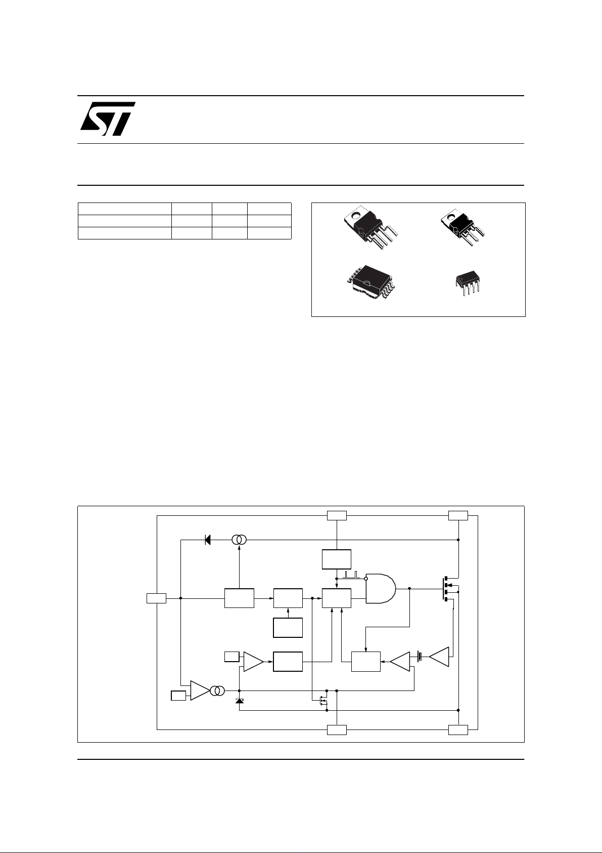
BLO C K DIAGRA M
PENTAWATT HV PENTAWATT HV (022Y)
10
1
PowerSO-10™
DIP-8
DESCRIPTION
VIPer20/20A, made using VIPower M0
Technology, combines on the same silicon chip a
state-of-the-art PWM circuit together with an
optimized high voltage avalanche rugged Vertical
Power MOSFET (620V or 700V / 0.5A).
Typical appli cations cover off line power supp lies
with a secondary power capability of 10W in wide
range conditio n and 20W in single range or with
doubler configuration. It is compatible from both
primary or secondary regulation loop despite
using around 50% less components when
compared with a discrete solution. Burst mode
operation is an additional featur e of this device ,
offering the possibility to operate in stand-by
mode without extra components.
_
CURRENT
AMPLIFIER
6 V/A
DRAIN
SOURCE
FC00491
VDD
13 V
_
+
ERROR
AMPLIFIER
0.5 V
UVLO
LOGIC
ON/OFF
+
_
4.5 V
SECURITY
LATCH
R/SSQ
OVERTEMP.
DETECTOR
delay
OSC
OSCILLATOR
PWM
LATCH
S
FFFF
R1
Q
R2 R3
0.5V
+
1.7
µ
s
COMP
250 ns
Blanking
+
_
July 2002 1/25
1
VIPer20/SP/DIP - VIPer20A/ASP/ADIP
ABSOLUTE MAXIMUM RATING
Symbol Parameter Value Unit
Continuous Drain-Source Voltage (Tj=25 to 125° C)
V
I
V
V
OSC
V
COMP
I
COMP
V
esd
for VIPer20/SP/DIP
DS
for VIPe r2 0A/ASP/ADIP
Maximum Current Internally limited A
D
Supply Voltage 0 to 15 V
DD
Voltage Range Input 0 to V
Voltage Range Input 0 to 5 V
Maximum Continuous Current ± 2mA
Electros tatic Discharge (R =1.5kΩ; C=100pF) 4000 V
Avalanche Drain-Sou rce Current, Repetitive or Not Repeti tive
I
D(AR)
(TC=100°C; Pulse width lim ited by Tj max; δ < 1%)
for VIPer20/SP/DIP
for VIPer20A/ASP/ADIP
P
T
T
Power Dissipation at Tc=25ºC57W
tot
Junction Operating Temperature Internally limited °C
j
Storage Temperature -65 to 150 °C
stg
THERMAL DATA
Symbol Parameter PENTAWATT PowerSO-10™ (*) DIP-8 Unit
R
thj-pin
R
thj-case
R
thj-amb.
(*) When mounted using the minim um r ec ommended pad siz e on FR-4 board.
(#) On multylayer PCB.
Thermal Resistance Junction-pin Max 20 °C/W
Thermal Resistance Junction-case Max 2.0 2.0 °C/W
Thermal Resistance Ambient-case Max 70 60 35 (#) °C/W
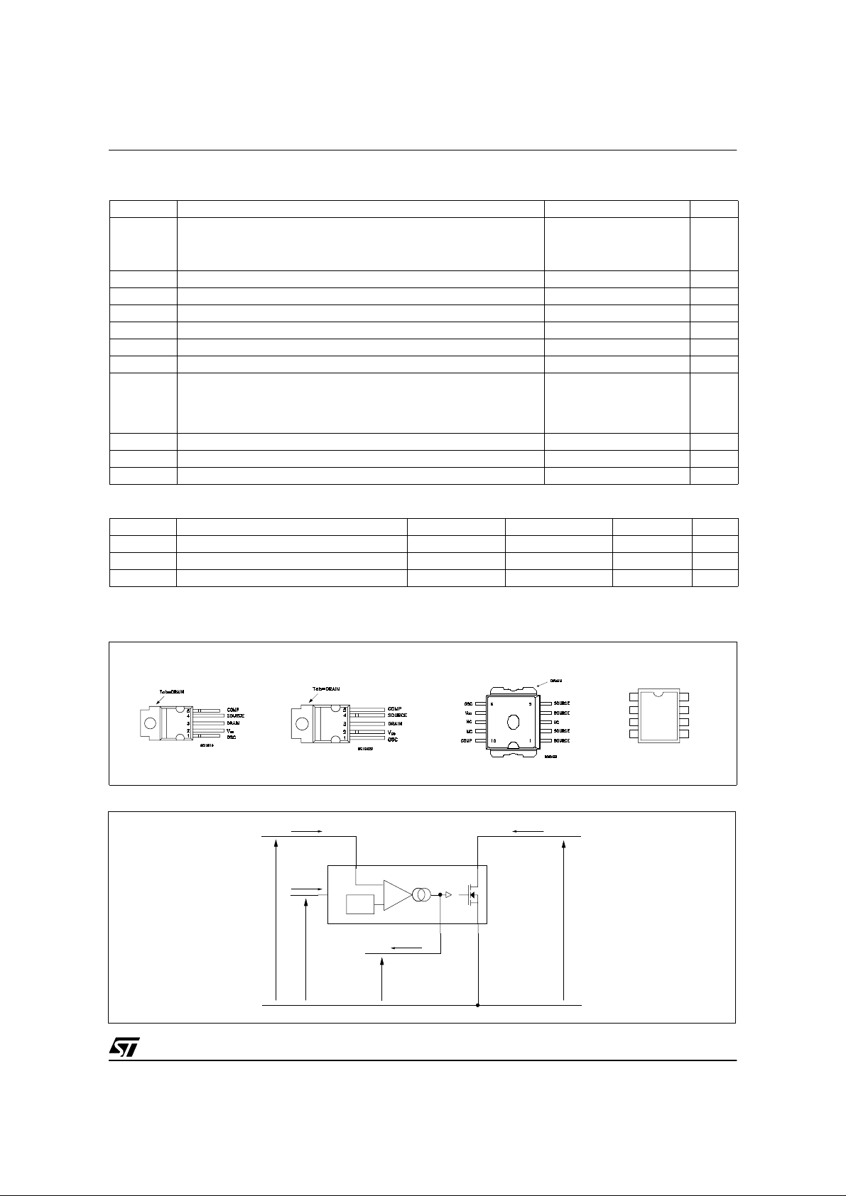
CONNECTION DIAGRAMS (Top View)
-0.3 to 620
-0.3 to 700
DD
0.5
0.4
V
V
V
A
A
PENTAWATT HV PENTAWATT HV (022Y) PowerSO -1 0™
CURRENT AND VOLTAGE CONVENTIONS
DD
I
OSC
I
OSC
DD
V
OSC
V
13V
+
COMP
I
COMP
V
DRAINVDD
COMP SOURCE
I
FC00020
DIP-8
OSC
148
Vdd
SOUR CE
COMP
D
DS
V
SC10540
DRAIN
DRAIN
DRAIN
5
DRAIN
2/25
1

VIPer20/SP/DIP - VIPer20A/ASP/ADIP
ORDERING NUMBERS
PENTAWATT HV PENTAWATT HV (022Y) PowerSO-10™ DIP-8
VIPer20 VIPer20 (022Y) VIPer20SP VIPer20DIP
VIPer20A VIPer20A ( 022Y) VIPer20ASP VIPer20ADIP
PINS FUNCTIONAL DESCRIPTION
DRAIN PIN:
Integrated Power MOSFET drain pin. It provide s
internal bias current during start-up via an
integrated high voltage current source which is
switched o ff during normal opera tion. The device
is able to handle an uncl amped current dur ing its
normal opera tion, assu ring self pr otectio n agains t
voltage surges, PCB stray inductance, and
allowing a snubberless operation for low output
power.
SOURCE Pin:
Power MOSFET source pin. Primary side circuit
common ground connection.
VDD Pin:
This pin provides two functions:
- It corresponds to th e low voltage su pply of the
control part of the circuit. If VDD goes below 8V,
the start-up cur rent sou rce is activ ate d and the
output power MOS FET is sw itc he d off until the
VDD voltage reache s 11V. During this phase,
the internal current consumption is reduced,
the VDD pin sources a current of about 2mA
and the COMP pin is shorted to ground. After
that, the curren t source is shut down, and the
device tries to start up by switching again.
- This pin is also connected to the error amplifier,
in order to all ow primary as wel l as secondar y
regulation configurations. In case of primary
regulation, an internal 13V trimme d reference
voltage is used to maintain VDD at 13V. For
secondary reg ulation, a voltag e between 8.5V
and 12.5V will be put on VDD pin by transformer
design, in order to stick the output of the
transconductance amplifier to the high state.
The COMP pin behaves as a constant current
source, and can easily be connected to the
output of an optocoupler. Note that any
overvoltage due to regulation loop failure is still
detected by the error amplifier through the V
voltage, which cannot overpass 13V. The
output voltage will be somewhat higher than the
nominal one, but still under control.
COMP PIN:
This pin provides two functions:
- It is the output of the error transconductance
amplifier, and allows for the connection of a
compensation network to provide the desired
transfer function of the regulation loop. Its
bandwidth can easily be adjusted to the
needed value with usual components value. As
stated above, secondary regulation
configurations are also implemented through
the COMP pin.
- When the COMP voltage goes bel ow 0.5V , the
shut-down of the circuit occurs, with a zero
duty cycle for the power MOSFET. This fea ture
can be used to sw itch off the converter, an d i s
automatically activ ated by the regulation l oop
(whatever is the configuration) to provide a
burst mode operation in case of negligible
output power or open load condition.
OSC PIN:
An Rt-Ct network must be connected on that pin to
define the swi tching frequen cy. Note tha t despite
the connection of Rt to VDD, no significant
frequency change oc curs for VDD varying from 8V
to 15V. It also provides a synchronization
capability, when connected to an external
frequency source.
DD
3/25
1
VIPer20/SP/DIP - VIPer20A/ASP/ADIP
AVALANCHE CHARACTERISTICS
Symbol Parameter Max Value Unit
Avalanch e Curr en t, Rep etitive or Not Repetitive
I
D(AR)
E
(ar)
(pulse widht limited by Tj max; δ < 1%)
for VIPe r20/SP/DIP
for VIPe r20A/ASP/ADIP (see fig.12)
Sing l e Pu lse Avalan ch e Energy
(starting Tj =25ºC, ID=I
) (see fig.12)
D(ar)
0.5
0.4
10 mJ
A
A
ELECTRICAL CHARACTERISTICS
(T
=25°C; VDD=13V, unless otherwise specified)
j
POWER SECTION
Symbol Parameter Test Conditions Min Typ Max Unit
BV
I
DSS
R
DS(on)
t
C
(1) On Induct iv e Load, Clamped.
Drain-Source Voltage
DSS
Off-State Drain Current
Static Drain-Source
On Resist ance
t
Fall Time
f
Rise Time
r
Output Capacitance VDS=25V 90 pF
oss
ID=1mA; V
for VIPer20/SP/DIP
for VIPer20A/ASP/ADIP (see fig.5)
V
=0V; Tj=125°C
COMP
VDS=620V for VIPer20/SP/DIP
VDS=700V for VIPer20A/ASP/ADIP
I
=0.4A
D
for VIPer20/SP/DIP
for VIPer20A/ASP/ADIP
=0.4A; Tj=100°C
I
D
for VIPer20/SP/DIP
for VIPer20A/ASP/ADIP
=0.2A; VIN=300V (1)
I
D
(See fig. 3)
=.4A; VIN=300V (1)
I
D
(See fig. 3)
COMP
=0V
620
700
1.0
1.0
13.5
15.5
16
18
29
32
100 ns
50 ns
SUPPLY SECTION
Symbol Parameter Test Conditions Min Typ Max Unit
I
DDch
I
DD0
I
DD1
I
DD2
V
DDoff
V
DDon
V
DDhyst
Start-Up Charging
Current
VDD=5V; VDS=35V
(see fig. 2 and fig. 15)
Oper at i ng Su pp ly Cu rrent VDD=12V; FSW=0kHz
(see fig. 2)
Oper at i ng Su pp ly Cu rrent VDD=12V; Fsw=100kHz 13 mA
Oper at i ng Su pp ly Cu rrent VDD=12V; Fsw=200kHz 14 mA
Undervoltage Shutdown (See fig. 2) 7.5 8 9 V
Undervoltage Reset (See fig. 2) 11 12 V
Hyst ere sis Start-up (See fig. 2) 2.4 3 V
-2 mA
12 16 mA
V
V
mA
mA
Ω
Ω
Ω
Ω
4/25
VIPer20/SP/DIP - VIPer20A/ASP/ADIP
ELECTRICAL CHARACTERISTICS (continued)
OSCILLATOR SECTION
Symbol Parameter Test Conditions Min Typ Max Unit
Rt=8.2KΩ; Ct=2.4nF
F
V
OSCih
V
OSCil
SW
Oscillat or Frequency
Total Variation
Oscillator Peak Voltage 7.1 V
Oscillator Valley Voltage 3.7 V
VDD=9 to 15V;
with R
± 1%; Ct± 5%
t
(see fig. 6 and fig. 9)
ERROR AMPLIFIER SECTIO N
Symbol Parameter Test Conditions Min Typ Max Unit
V
DDreg
∆V
DDreg
G
A
VOL
G
V
COMPLO
V
COMPHI
I
COMPLO
I
COMPHI
VDD Regulati on Point I
=0mA (see fig. 1) 12.6 13 13.4 V
COMP
Total Variation Tj=0 to 100°C 2 %
Unity Gain Bandwidth
BW
From Input =VDD to Output = V
COMP pin is open (see fig. 10)
COMP
Open Loop Voltage Gai n COMP pin is open (see fig. 10) 45 52 dB
DC Transconductance V
m
Output Low Level I
Output High Level I
Output Low Current
Capability
Output High Current
Capability
=2.5V (see fig. 1) 1.1 1.5 1.9 mA/V
COMP
= -400µA; VDD=14V 0.2 V
COMP
=400µA; VDD=12V 4.5 V
COMP
V
=2.5V; VDD=14V -600 µA
COMP
V
=2.5V; VDD=12V 600 µA
COMP
90 100 110 kHz
150 kHz
PWM COMPARATOR SECTION
Symbol Parameter Test Conditions Min Typ Max Unit
H
V
COMPoffVCOMP
I
Dpeak
t
t
t
on(min)
∆V
ID
/ ∆I
COMP
DPEAK
Offs et I
V
=1 to 3 V 4.267.8V/A
COMP
=10mA 0.5 V
DPEAK
Peak Current Limitation VDD=12V; COMP pin open 0.5 0.67 0.9 A
Current Sense Delay to
d
Turn-Off
Blanking Time 250 360 ns
b
ID=1A 250 ns
Minimum On Time 350 ns
SHUTDOWN AND OVERTEMPERATURE SECTION
Symbol Parameter Test Conditions Min Typ Max Unit
V
COMPth
t
DISsu
T
T
hyst
Restart Th reshold (see fig. 4) 0.5 V
Disable Set Up Time (see fig. 4) 1.7 5 µs
Ther ma l Shutdow n
tsd
Temperature
Ther ma l Shutdow n
Hysteresis
(See fig. 8) 140 170 190 °C
(See fig. 8) 40 °C
5/25
VIPer20/SP/DIP - VIPer20A/ASP/ADIP
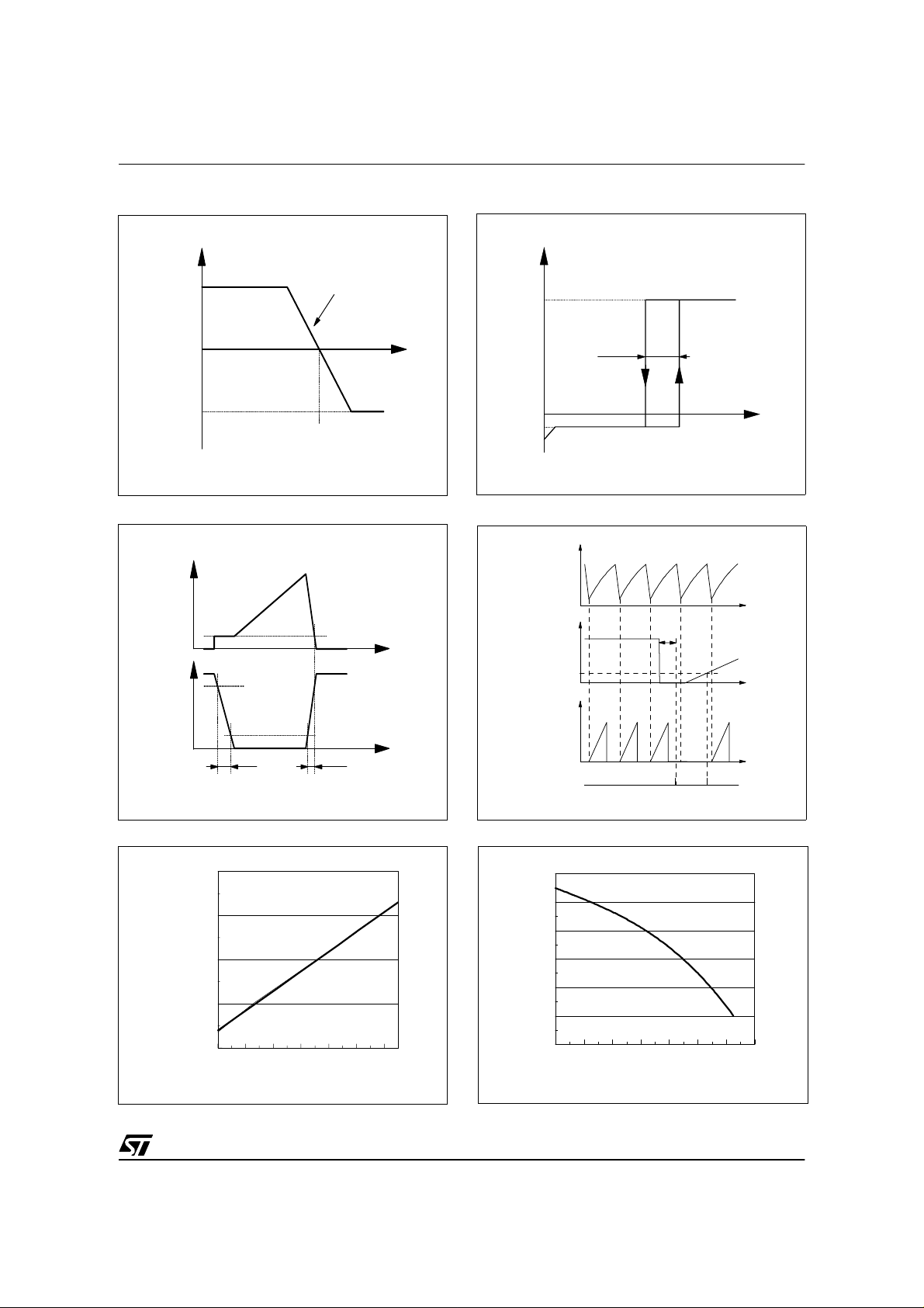
Figure 1: VDD Regulation Point
ICOM P
ICOMPHI
0
ICOMPLO
VDDreg
Figure 3: Transition Time
I
D
10% Ipeak
Slope =
Gm in mA/V
FC00150
Figure 2: Undervoltage Lockout
I
DD
I
DD0
VDD
VDDhyst
VDDoff
VDS= 35 V
Fsw = 0
VDDon
V
DD
IDDch
FC00170
Figure 4: Shut Down Action
VOSC
t
VCOMP
t
tDISsu
V
DS
90% V
10% V
tf
D
D
t
tr
FC00160
VCOMPth
ID
ENABLE
DISA BLE
Figure 5: Breakdown Voltage Vs. Temperature Figure 6: Typi cal Frequency Variation
1.15
BVDSS
(Normalized)
1.05
0.95
1.1
1
0 20406080100120
Temperature (°C )
FC00180
1
(%)
0
-1
-2
-3
-4
-5
0 20406080100120140
Temperature (°C)
t
t
ENABLE
FC00060
FC00190
6/25
VIPer20/SP/DIP - VIPer20A/ASP/ADIP
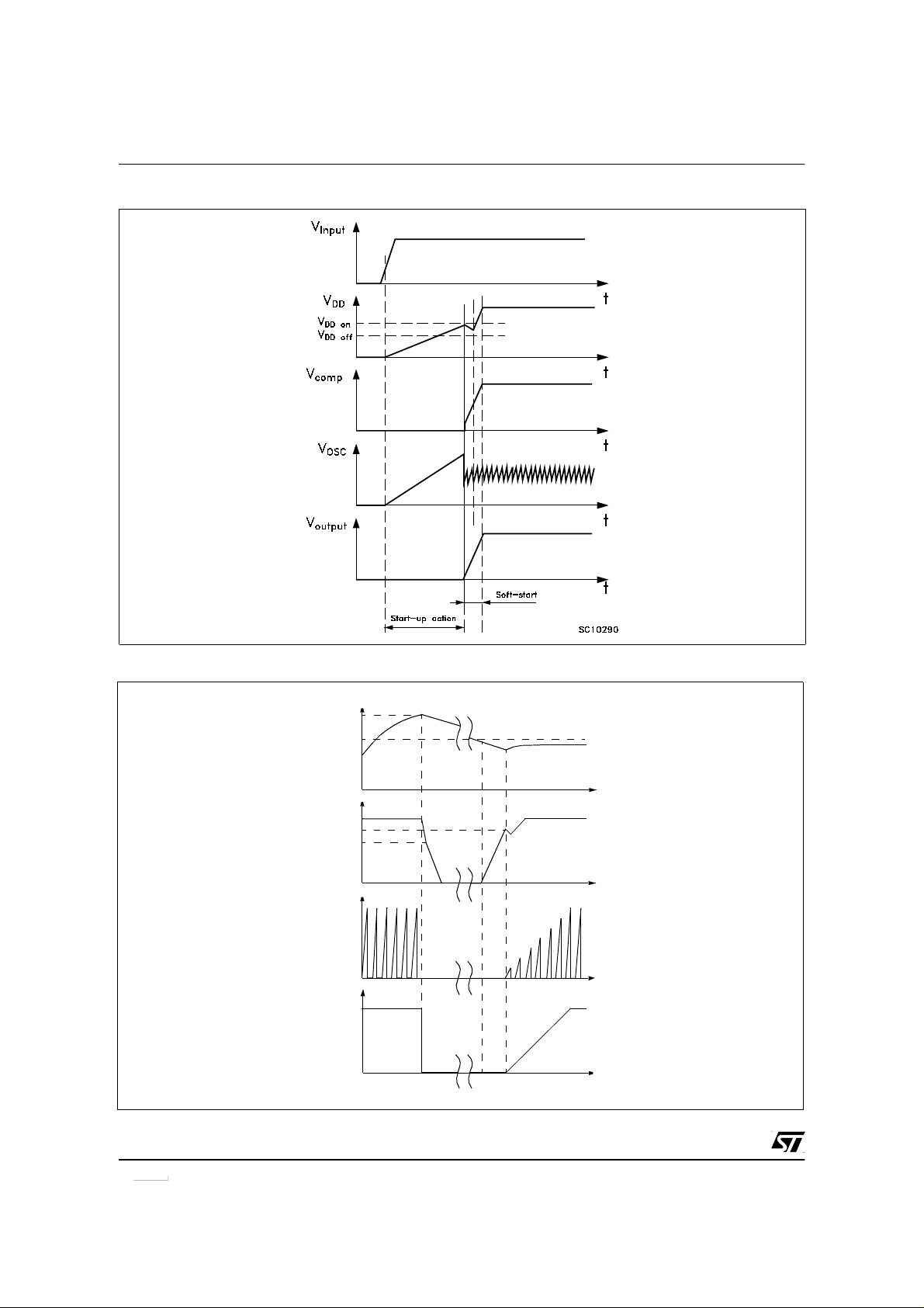
Figur e 7: Start-Up Waveforms
Figure 8: Overtemperature Protection
T
T
tsd-Thyst
V
ddon
V
ddoff
V
comp
tsc
V
T
dd
I
J
t
t
d
t
t
SC10191
7/25
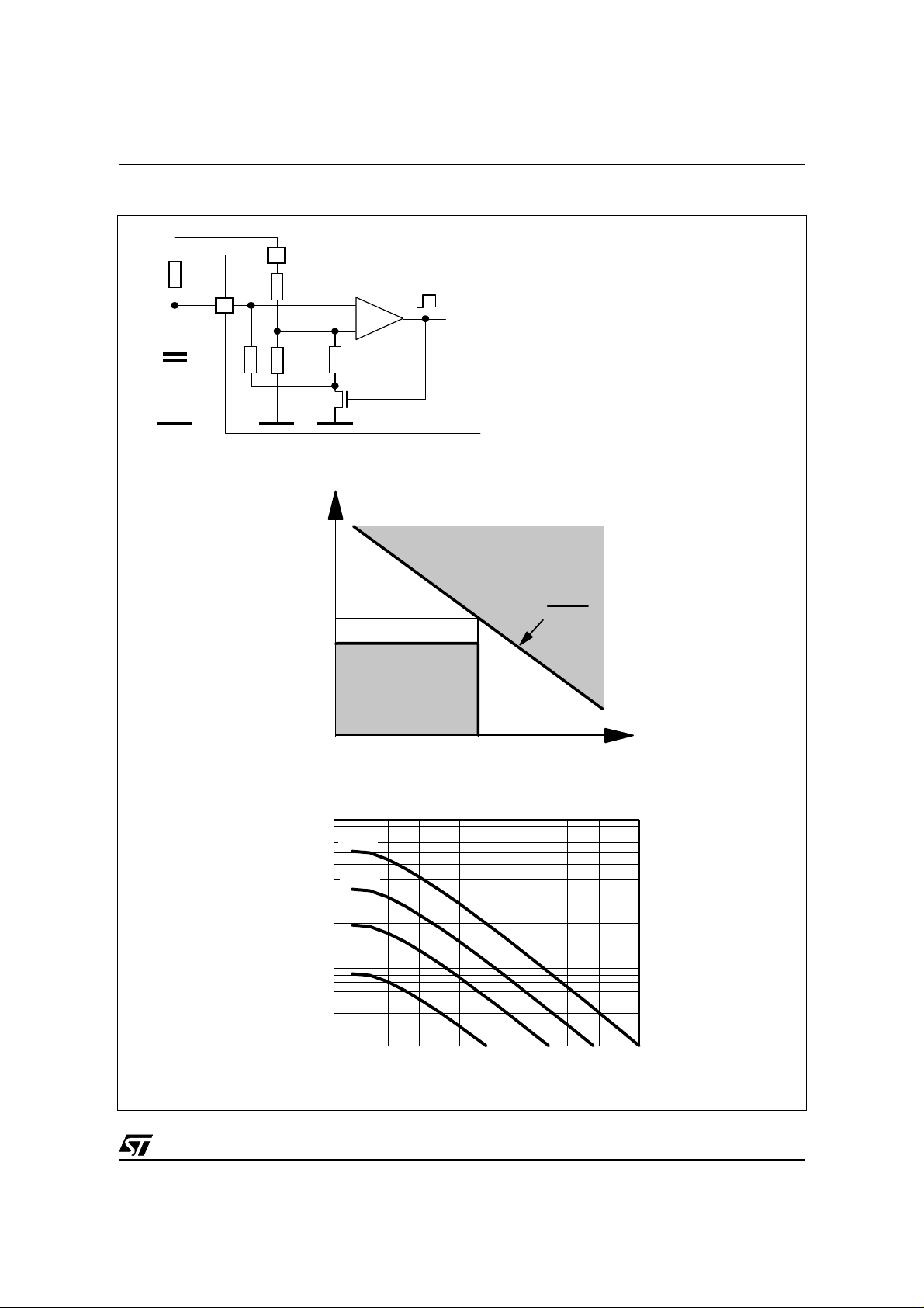
Figur e 9: Oscillator
VIPer20/SP/DIP - VIPer20A/ASP/ADIP
Ct
Rt
OSC
~360Ω
VDD
C
t
22nF
15nF
FC00050
Forbidden area
CLK
Forbidden area
For Rt >1.2KΩ
and
Ct ≥ 15nF if FSW ≤ 40KHz
F
SW
Ct(nF) =
2.3
------------
=
880
Fsw(kHz)
⋅
RtC
t
550
----------------------
–
1
Rt150
–
40kHz
Fsw
Oscillator frequency vs Rt and Ct
1,000
500
300
200
100
Ct = 1.5 nF
Ct = 2.7 nF
Ct = 4.7 nF
Ct = 10 nF
FC00030FC00030
Frequency (kHz)
50
30
1 2 3 5 10 20 30 50
Rt (kΩ)
8/25
1
 Loading...