

Page 1
Introduction
The STM32H7 Nucleo-144 boards based on the MB1364 reference board (NUCLEOH723ZG, NUCLEO-H743ZI (Order code NUCLEO-H743ZI2), and NUCLEO-H753ZI)
provide an affordable and flexible way for users to try out new concepts and build
prototypes, by choosing from the various combinations of performance and power
consumption features provided by the STM32H7 Series microcontroller. The ST Zio
connector, which extends the ARDUINO
provide an easy means of expanding the functionality of the Nucleo open development
platform with a wide choice of specialized shields. The STM32H7 Nucleo-144 boards do not
require any separate probe as they integrate the STLINK-V3 debugger/programmer. The
STM32H7 Nucleo-144 boards come with the comprehensive free software libraries and
examples available with the STM32Cube MCU Package.
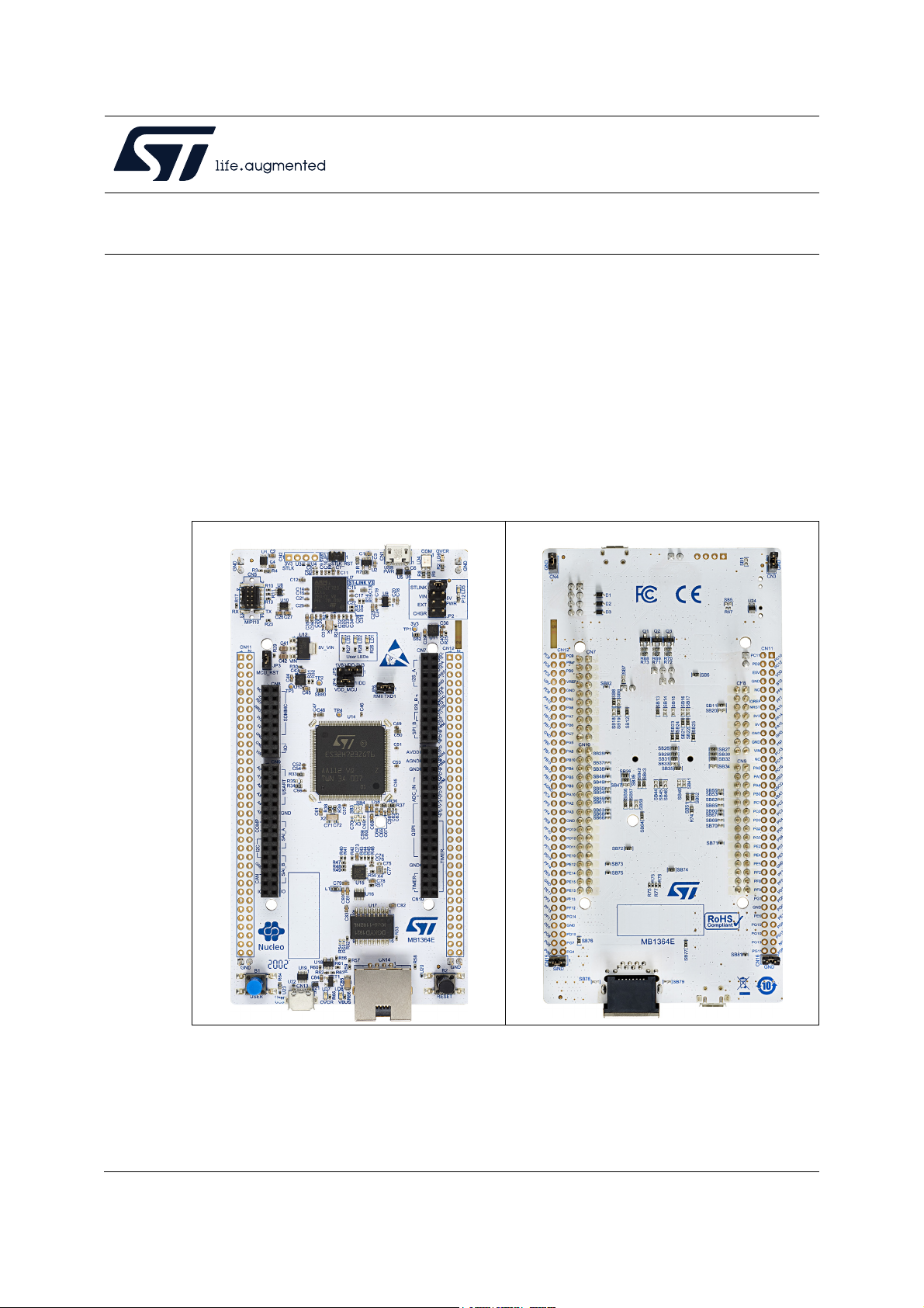
Figure 1. Nucleo-144 board (top view) Figure 2. Nucleo-144 board (bottom view)
UM2407
User manual
STM32H7 Nucleo-144 boards (MB1364)
®
Uno V3 connectivity, and the ST morpho headers
Pictures are not contractual.
June 2020 UM2407 Rev 2 1/50
www.st.com
1
Page 2
Contents UM2407
Contents
1 Features . . . . . . . . . . . . . . . . . . . . . . . . . . . . . . . . . . . . . . . . . . . . . . . . . . . 6
2 Ordering information . . . . . . . . . . . . . . . . . . . . . . . . . . . . . . . . . . . . . . . . 7
2.1 Codification . . . . . . . . . . . . . . . . . . . . . . . . . . . . . . . . . . . . . . . . . . . . . . . . . 7
3 Development environment . . . . . . . . . . . . . . . . . . . . . . . . . . . . . . . . . . . . 8
3.1 Development toolchains . . . . . . . . . . . . . . . . . . . . . . . . . . . . . . . . . . . . . . . 8
3.2 System requirements . . . . . . . . . . . . . . . . . . . . . . . . . . . . . . . . . . . . . . . . . 8
3.3 Demonstration software . . . . . . . . . . . . . . . . . . . . . . . . . . . . . . . . . . . . . . . 8
4 Conventions . . . . . . . . . . . . . . . . . . . . . . . . . . . . . . . . . . . . . . . . . . . . . . . . 9
5 Quick start . . . . . . . . . . . . . . . . . . . . . . . . . . . . . . . . . . . . . . . . . . . . . . . . 10
5.1 Getting started . . . . . . . . . . . . . . . . . . . . . . . . . . . . . . . . . . . . . . . . . . . . . 10
6 Hardware layout and configuration . . . . . . . . . . . . . . . . . . . . . . . . . . . . 11
6.1 Nucleo-144 board layout . . . . . . . . . . . . . . . . . . . . . . . . . . . . . . . . . . . . . 12
6.2 Mechanical drawing . . . . . . . . . . . . . . . . . . . . . . . . . . . . . . . . . . . . . . . . . 14
6.3 Embedded STLINK-V3E . . . . . . . . . . . . . . . . . . . . . . . . . . . . . . . . . . . . . 16
6.3.1 Drivers . . . . . . . . . . . . . . . . . . . . . . . . . . . . . . . . . . . . . . . . . . . . . . . . . . 16
6.3.2 STLINK-V3E firmware upgrade . . . . . . . . . . . . . . . . . . . . . . . . . . . . . . . 17
6.3.3 Using an external debug tool to program and debug the on-boards
STM32H7 . . . . . . . . . . . . . . . . . . . . . . . . . . . . . . . . . . . . . . . . . . . . . . . . 17
6.4 Power supply . . . . . . . . . . . . . . . . . . . . . . . . . . . . . . . . . . . . . . . . . . . . . . 19
6.4.1 Power supply input from STLINK-V3E USB connector (default setting) 19
6.4.2 External power supply input from VIN (7 V to 12 V, 800 mA max) . . . . . 20
6.4.3 External power supply input 5V_EXT (5 V, 500 mA max) . . . . . . . . . . . 21
6.4.4 External power supply input from USB CHARGER (5 V) . . . . . . . . . . . 22
6.4.5 External power supply input from 3V3_EXT (3.3 V) . . . . . . . . . . . . . . . 22
6.4.6 Debugging while using VIN or EXT as an external power supply . . . . . 23
6.5 Clock sources . . . . . . . . . . . . . . . . . . . . . . . . . . . . . . . . . . . . . . . . . . . . . . 24
6.5.1 HSE clock (high-speed external clock) . . . . . . . . . . . . . . . . . . . . . . . . . 24
6.5.2 LSE clock (low-speed external clock) - 32.768 kHz . . . . . . . . . . . . . . . . 24
6.6 Board functions . . . . . . . . . . . . . . . . . . . . . . . . . . . . . . . . . . . . . . . . . . . . 25
2/50 UM2407 Rev 2
Page 3
UM2407 Contents
6.6.1 LEDs . . . . . . . . . . . . . . . . . . . . . . . . . . . . . . . . . . . . . . . . . . . . . . . . . . . 25
6.6.2 Push-buttons . . . . . . . . . . . . . . . . . . . . . . . . . . . . . . . . . . . . . . . . . . . . . 26
6.6.3 MCU voltage selection: 1V8/3V3 . . . . . . . . . . . . . . . . . . . . . . . . . . . . . . 26
6.6.4 Current consumption measurement (IDD) . . . . . . . . . . . . . . . . . . . . . . . 26
6.6.5 Virtual COM port (VCP): LPUART/USART . . . . . . . . . . . . . . . . . . . . . . 26
6.6.6 USB OTG FS . . . . . . . . . . . . . . . . . . . . . . . . . . . . . . . . . . . . . . . . . . . . . 27
6.6.7 Ethernet . . . . . . . . . . . . . . . . . . . . . . . . . . . . . . . . . . . . . . . . . . . . . . . . . 28
6.7 Solder bridges and jumpers . . . . . . . . . . . . . . . . . . . . . . . . . . . . . . . . . . . 29
7 Board connectors . . . . . . . . . . . . . . . . . . . . . . . . . . . . . . . . . . . . . . . . . . 34
7.1 STLINK-V3 USB Micro-B connector CN1 . . . . . . . . . . . . . . . . . . . . . . . . 34
7.2 USB OTG FS connector CN13 . . . . . . . . . . . . . . . . . . . . . . . . . . . . . . . . . 35
7.3 Ethernet RJ45 connector CN14 . . . . . . . . . . . . . . . . . . . . . . . . . . . . . . . . 35
8 Extension connectors . . . . . . . . . . . . . . . . . . . . . . . . . . . . . . . . . . . . . . . 37
8.1 ST Zio connectors . . . . . . . . . . . . . . . . . . . . . . . . . . . . . . . . . . . . . . . . . . 37
8.2 ST morpho connector . . . . . . . . . . . . . . . . . . . . . . . . . . . . . . . . . . . . . . . . 42
9 Nucleo-144 boards information . . . . . . . . . . . . . . . . . . . . . . . . . . . . . . . 44
9.1 Product marking . . . . . . . . . . . . . . . . . . . . . . . . . . . . . . . . . . . . . . . . . . . . 44
9.2 Board revision history . . . . . . . . . . . . . . . . . . . . . . . . . . . . . . . . . . . . . . . . 44
9.3 Known limitations . . . . . . . . . . . . . . . . . . . . . . . . . . . . . . . . . . . . . . . . . . . 45
Appendix A Federal Communications Commission (FCC)
and ISED Canada (IC) Compliance Statements . . . . . . . . . . . . . . . 46
A.1 FCC Compliance Statement . . . . . . . . . . . . . . . . . . . . . . . . . . . . . . . . . . . 46
A.2 ISED Compliance Statement. . . . . . . . . . . . . . . . . . . . . . . . . . . . . . . . . . . 46
Appendix B CE conformity . . . . . . . . . . . . . . . . . . . . . . . . . . . . . . . . . . . . . . . . . . 48
B.1 Warning. . . . . . . . . . . . . . . . . . . . . . . . . . . . . . . . . . . . . . . . . . . . . . . . . . . 48
Revision history . . . . . . . . . . . . . . . . . . . . . . . . . . . . . . . . . . . . . . . . . . . . . . . . . . . . 49
UM2407 Rev 2 3/50
3
Page 4

List of tables UM2407
List of tables
Table 1. Ordering information . . . . . . . . . . . . . . . . . . . . . . . . . . . . . . . . . . . . . . . . . . . . . . . . . . . . . . . 7
Table 2. Codification explanation . . . . . . . . . . . . . . . . . . . . . . . . . . . . . . . . . . . . . . . . . . . . . . . . . . . . 7
Table 3. ON/OFF conventions . . . . . . . . . . . . . . . . . . . . . . . . . . . . . . . . . . . . . . . . . . . . . . . . . . . . . . 9
Table 4. Jumper configuration . . . . . . . . . . . . . . . . . . . . . . . . . . . . . . . . . . . . . . . . . . . . . . . . . . . . . 10
Table 5. MIPI-10 debug connector (CN5) . . . . . . . . . . . . . . . . . . . . . . . . . . . . . . . . . . . . . . . . . . . . . 18
Table 6. External power sources: VIN (7 V to 12 V). . . . . . . . . . . . . . . . . . . . . . . . . . . . . . . . . . . . . 21
Table 7. External power sources: 5V_EXT. . . . . . . . . . . . . . . . . . . . . . . . . . . . . . . . . . . . . . . . . . . . 21
Table 8. External power sources: CHGR (5 V). . . . . . . . . . . . . . . . . . . . . . . . . . . . . . . . . . . . . . . . . 22
Table 9. External power sources: 3V3_EXT (3.3 V). . . . . . . . . . . . . . . . . . . . . . . . . . . . . . . . . . . . . 23
Table 10. USART3 connection . . . . . . . . . . . . . . . . . . . . . . . . . . . . . . . . . . . . . . . . . . . . . . . . . . . . . . 27
Table 11. LPUART1 connection . . . . . . . . . . . . . . . . . . . . . . . . . . . . . . . . . . . . . . . . . . . . . . . . . . . . . 27
Table 12. USB pin configuration . . . . . . . . . . . . . . . . . . . . . . . . . . . . . . . . . . . . . . . . . . . . . . . . . . . . . 28
Table 13. Ethernet pin configuration. . . . . . . . . . . . . . . . . . . . . . . . . . . . . . . . . . . . . . . . . . . . . . . . . . 28
Table 14. Solder bridge and jumper configuration . . . . . . . . . . . . . . . . . . . . . . . . . . . . . . . . . . . . . . . 29
Table 15. USB Micro-B connector pinout . . . . . . . . . . . . . . . . . . . . . . . . . . . . . . . . . . . . . . . . . . . . . . 34
Table 16. USB OTG FS Micro-AB connector pinout. . . . . . . . . . . . . . . . . . . . . . . . . . . . . . . . . . . . . . 35
Table 17. Ethernet connector pinout. . . . . . . . . . . . . . . . . . . . . . . . . . . . . . . . . . . . . . . . . . . . . . . . . . 36
Table 18. CN7 ZIO connector pinout . . . . . . . . . . . . . . . . . . . . . . . . . . . . . . . . . . . . . . . . . . . . . . . . . 39
Table 19. CN8 ZIO connector pinout . . . . . . . . . . . . . . . . . . . . . . . . . . . . . . . . . . . . . . . . . . . . . . . . . 39
Table 20. CN9 ZIO connector pinout . . . . . . . . . . . . . . . . . . . . . . . . . . . . . . . . . . . . . . . . . . . . . . . . . 40
Table 21. CN10 ZIO connector pinout . . . . . . . . . . . . . . . . . . . . . . . . . . . . . . . . . . . . . . . . . . . . . . . . 41
Table 22. ST morpho connector pin assignment . . . . . . . . . . . . . . . . . . . . . . . . . . . . . . . . . . . . . . . . 42
Table 23. Document revision history . . . . . . . . . . . . . . . . . . . . . . . . . . . . . . . . . . . . . . . . . . . . . . . . . 49
4/50 UM2407 Rev 2
Page 5

UM2407 List of figures
List of figures
Figure 1. Nucleo-144 board (top view). . . . . . . . . . . . . . . . . . . . . . . . . . . . . . . . . . . . . . . . . . . . . . . . . 1
Figure 2. Nucleo-144 board (bottom view). . . . . . . . . . . . . . . . . . . . . . . . . . . . . . . . . . . . . . . . . . . . . . 1
Figure 3. Hardware block diagram. . . . . . . . . . . . . . . . . . . . . . . . . . . . . . . . . . . . . . . . . . . . . . . . . . . 11
Figure 4. Nucleo-144 board top layout. . . . . . . . . . . . . . . . . . . . . . . . . . . . . . . . . . . . . . . . . . . . . . . . 12
Figure 5. Nucleo-144 bottom layout. . . . . . . . . . . . . . . . . . . . . . . . . . . . . . . . . . . . . . . . . . . . . . . . . . 13
Figure 6. Nucleo-144 board mechanical drawing in millimeter . . . . . . . . . . . . . . . . . . . . . . . . . . . . . 14
Figure 7. Nucleo-144 board mechanical drawing in mil . . . . . . . . . . . . . . . . . . . . . . . . . . . . . . . . . . . 15
Figure 8. USB composite device . . . . . . . . . . . . . . . . . . . . . . . . . . . . . . . . . . . . . . . . . . . . . . . . . . . . 17
Figure 9. Connecting an external debug tool to program the on-board STM32H7 . . . . . . . . . . . . . . 18
Figure 10. Power supply input from STLINK-V3E USB connector with PC (5 V, 500 mA max) . . . . . 20
Figure 11. Power supply input from VIN (7 V to 12 V, 800 mA max). . . . . . . . . . . . . . . . . . . . . . . . . . 21
Figure 12. Power supply input from 5V_EXT (5 V, 500 mA max) . . . . . . . . . . . . . . . . . . . . . . . . . . . . 22
Figure 13. Power supply input from STLINK-V3E USB connector with a USB charger (5 V) . . . . . . . 22
Figure 14. Power supply input from 3V3_EXT (3.3 V) . . . . . . . . . . . . . . . . . . . . . . . . . . . . . . . . . . . . . 23
Figure 15. USB Micro-B connector CN1 (front view) . . . . . . . . . . . . . . . . . . . . . . . . . . . . . . . . . . . . . . 34
Figure 16. USB OTG FS Micro-AB connector CN13 (front view). . . . . . . . . . . . . . . . . . . . . . . . . . . . . 35
Figure 17. Ethernet RJ45 connector CN14 (front view). . . . . . . . . . . . . . . . . . . . . . . . . . . . . . . . . . . . 36
Figure 18. NUCLEOH7 Nucleo-144 board. . . . . . . . . . . . . . . . . . . . . . . . . . . . . . . . . . . . . . . . . . . . . . 37
UM2407 Rev 2 5/50
5
Page 6
Features UM2407
1 Features
The STM32H7 Nucleo-144 boards offer the following features:
• STM32H7 Arm
• Ethernet compliant with IEEE-802.3-2002 (depending on STM32H7 support)
• USB OTG full-speed
• 3 user LEDs
• 2 push-buttons: USER and RESET
• LSE crystal:
– 32.768 kHz crystal oscillator
• Board connectors:
– USB with Micro-AB
– Ethernet RJ45
–MIPI10
• Board expansion connectors:
– ST Zio including ARDUINO
–ST morpho
• Flexible power-supply options: ST-LINK USB V
• On-board STLINK-V3 debugger/programmer with SWD connector:
– USB re-enumeration capability: virtual COM port, mass storage, debug port
– STLINK-V3 standalone kit capability
• Comprehensive free software libraries and examples available with the STM32Cube
package
• Support of a wide choice of Integrated Development Environments (IDEs) including
IAR Embedded Workbench
®(a)
Cortex® core-based microcontroller in LQFP144 package
®
Uno V3
or external sources
BUS
®
, MDK-ARM, and STM32CubeIDE
a. Arm is a registered trademark of Arm Limited (or its subsidiaries) in the US and/or elsewhere.
6/50 UM2407 Rev 2
Page 7
UM2407 Ordering information
2 Ordering information
To order the Nucleo-144 board corresponding to the targeted STM32, use the order code
given below in
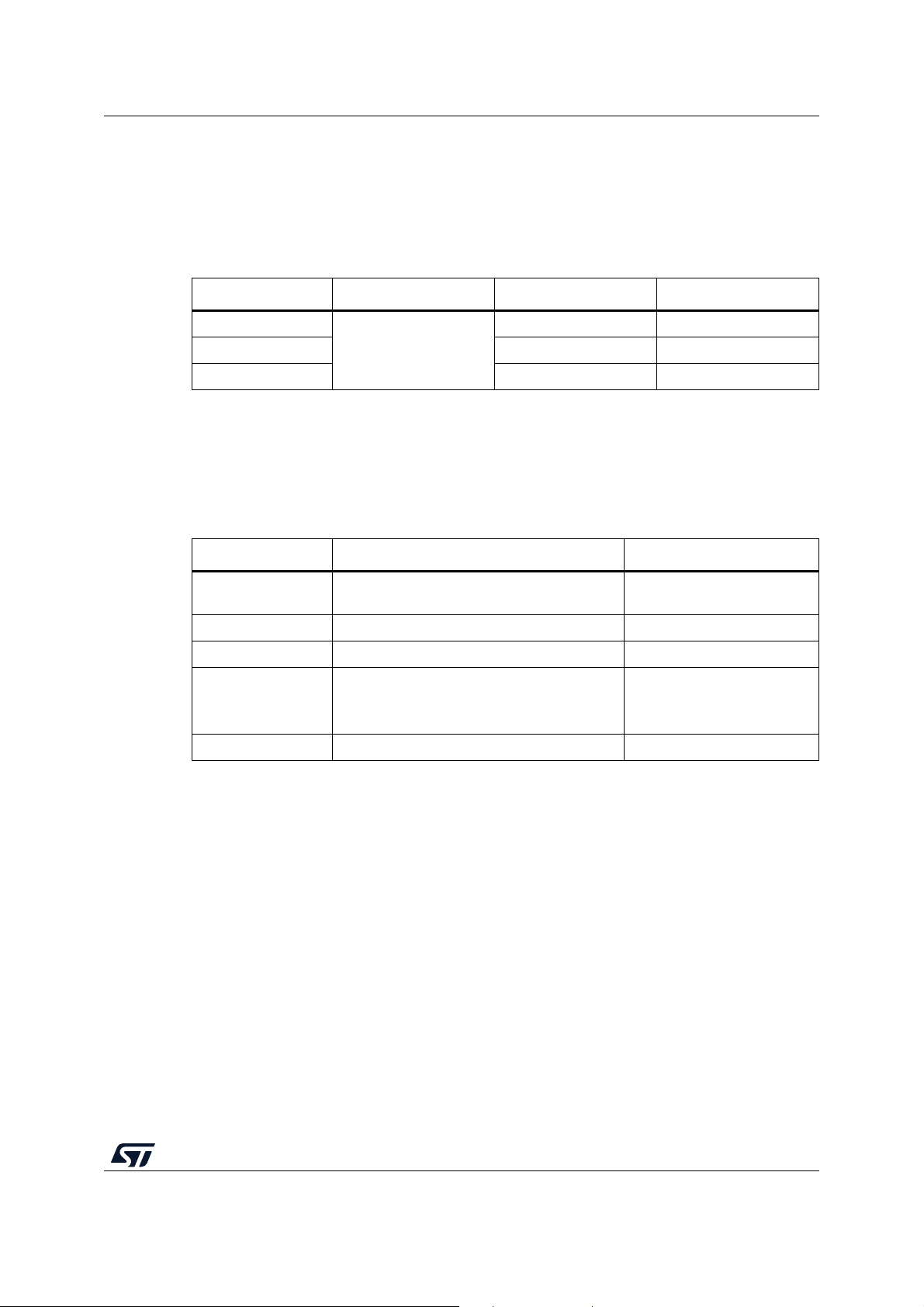
Order code Board reference Target STM32H7 Differentiating feature
Table 1:
Table 1. Ordering information
NUCLEO-H723ZG
NUCLEO-H743ZI2 STM32H743ZIT6U -
NUCLEO-H753ZI STM32H753ZIT6U Cryptography
2.1 Codification
The meaning of the codification is explained in Tabl e 2. The order code is mentioned on a
sticker placed on the top or bottom side of the board.
NUCLEO-XXYYZTN Description Example: NUCLEO-H743ZI2
XX
YY MCU product line in the series STM32H743
Z STM32 package pin count 144 pins
T
N Board version: void or 2 STLINK-V3E
STM32H723ZGT6U -
MB1364
Table 2. Codification explanation
MCU series in STM32 32-bit Arm Cortex
MCUs
STM32H7 Flash memory size:
-G for 1 Mbyte
-I for 2 Mbytes
STM32H7 Series
2 Mbytes
UM2407 Rev 2 7/50
49
Page 8
Development environment UM2407
3 Development environment
3.1 Development toolchains
• IAR Systems - IAR Embedded Workbench
• Keil® - MDK-ARM
• STMicroelectronics - STM32CubeIDE
(a)
3.2 System requirements
• Windows® OS (7, 8 and 10), Linux® or macOS
• USB Type-A to Micro-B cable
3.3 Demonstration software
The demonstration software, included in the STM32Cube package, is preloaded in the
STM32H7 Flash memory for easy demonstration of the device peripherals in standalone
mode. The latest versions of the demonstration source code and associated documentation
can be downloaded from the www.st.com/stm32nucleo web page.
®(a)
®(b)
a. On Windows only.
b. macOS is a trademark of Apple Inc., registered in the U.S. and other countries.
8/50 UM2407 Rev 2
Page 9
UM2407 Conventions
4 Conventions
Table 3 provides the conventions used for the ON and OFF settings in the present
document.
Convention Definition
Jumper JPx ON Jumper fitted
Jumper JPx OFF Jumper not fitted
Solder bridge SBx ON SBx connections closed by solder or 0-ohm resistor
Solder bridge SBx OFF SBx connections left open
In this document, for any information that is common to all sales types, the references are
noted “STM32H7 Nucleo-144 board” and “STM32H7 Nucleo-144 boards”.
Table 3. ON/OFF conventions
UM2407 Rev 2 9/50
49
Page 10
Quick start UM2407
5 Quick start
The STM32H7 Nucleo-144 board is a low-cost and easy-to-use development kit, used to
evaluate and start development quickly with an STM32H7 Series microcontroller in
LQFP144 package.
Before installing and using the product, accept the Evaluation Product License Agreement
from the www.st.com/epla web page. For more information on the STM32H7 Nucleo-144
and for demonstration software, visit the www.st.com/stm32nucleo
5.1 Getting started
Follow the sequence below to configure the Nucleo-144 board and launch the
demonstration application (for components location, refer to
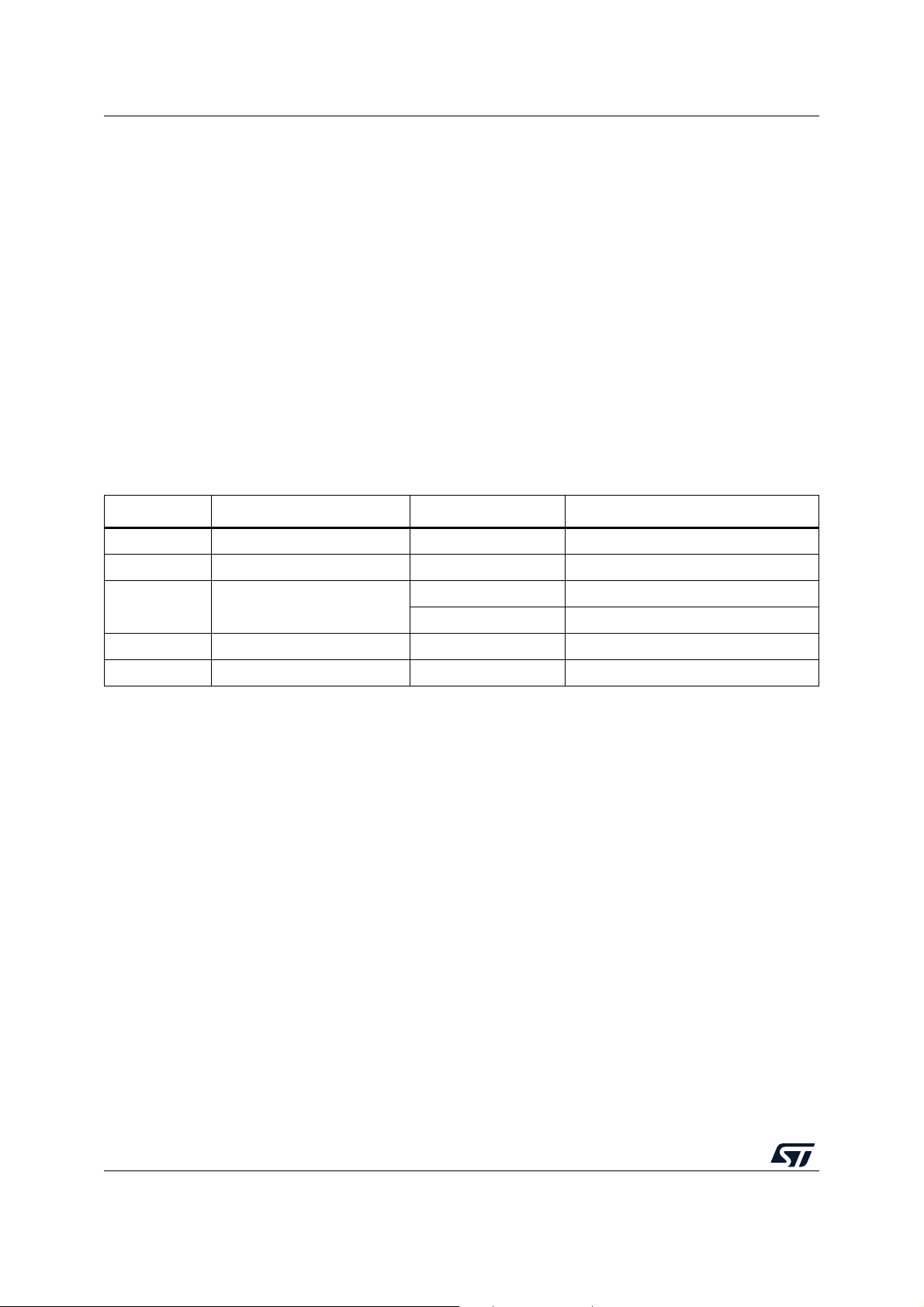
1. Check jumper position on the board:
Jumper Definition Position Comment
JP1 STLK_RST OFF -
JP3 T_NRST ON -
JP5 VDD_MCU power selection
JP4 IDD measurement ON MCU current measurement
JP2 Power source selection ON [1-2] 5V_USB_STLK (from ST-LINK)
Table 4. Jumper configuration
ON [1-2] (default) VDD_MCU supplied with 3V3_VDD
ON [2-3] (optional) VDD_MCU supplied with 1V8_VDD
web page.
Figure 4):
2. For the correct identification of the device interfaces from the host PC and before
connecting the board, install the Nucleo USB driver available on the
www.st.com/stm32nucleo website.
3. Power the board by connecting the STM32H7 Nucleo-144 board to a PC with a USB
cable ‘Type-A to Micro-B’ through the USB connector CN1 on the ST-LINK. As a result,
the green LED LD6 (PWR) and LD4 (COM) light up and the red LED LD3 blinks.
4. Press button B1 (left button).
5. Observe the blinking frequency of the three LEDs LD1 to LD3 changes, by clicking on
the button B1.
6. The software demonstration and the several software examples, that allow the user to
use the Nucleo features, are available at the www.st.com/stm32nucleo web page.
7. Develop an application, using the available examples.
10/50 UM2407 Rev 2
Page 11
UM2407 Hardware layout and configuration
MSv51396V1
Embedded
STLINK-V3E
STM32
Microcontroller
ST morpho extension header
ST morpho extension header
IO
VCP
UART
B2
reset
button
B1
user
button
IO
Zio Connector
ST-LINK part
MCU part
LED1
LED2
LED3
Micro-AB
USB
connector
Zio Connector
RJ45
connector
Micro-B
USB
connector
SWD
SWD
VCP
UART
USB RMII
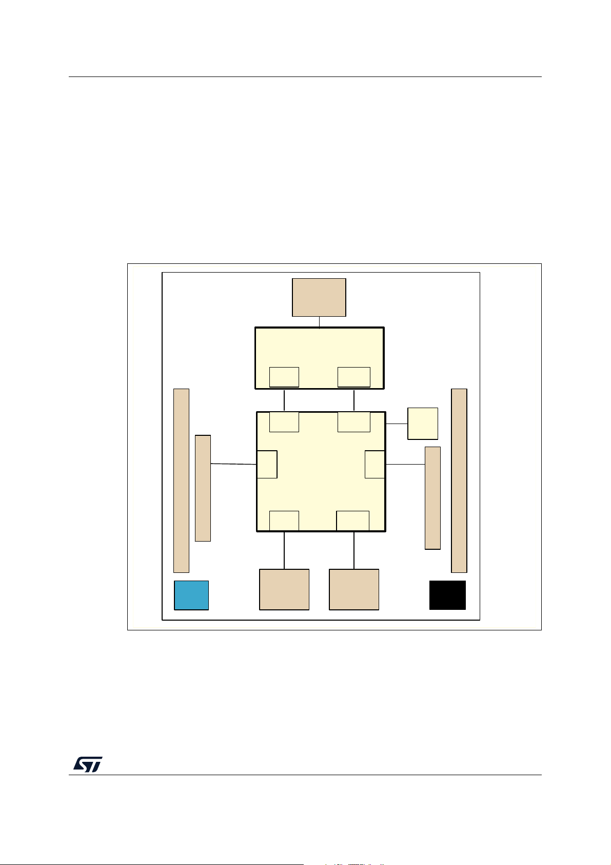
6 Hardware layout and configuration
The STM32H7 Nucleo-144 board is designed around the STM32H7 Series microcontrollers
in a 144-pin LQFP package.
Figure 3 shows the connections between the STM32H7 and its peripherals (STLINK-V3E,
push-buttons, LEDs, USB, Ethernet, ST Zio connectors, and ST morpho headers).
Figure 4 and Figure 5 show the location of these features on the STM32H7 Nucleo-144
board.
The mechanical dimensions of the board are shown in Figure 6 and Figure 7.
Figure 3. Hardware block diagram
UM2407 Rev 2 11/50
49
Page 12
Hardware layout and configuration UM2407
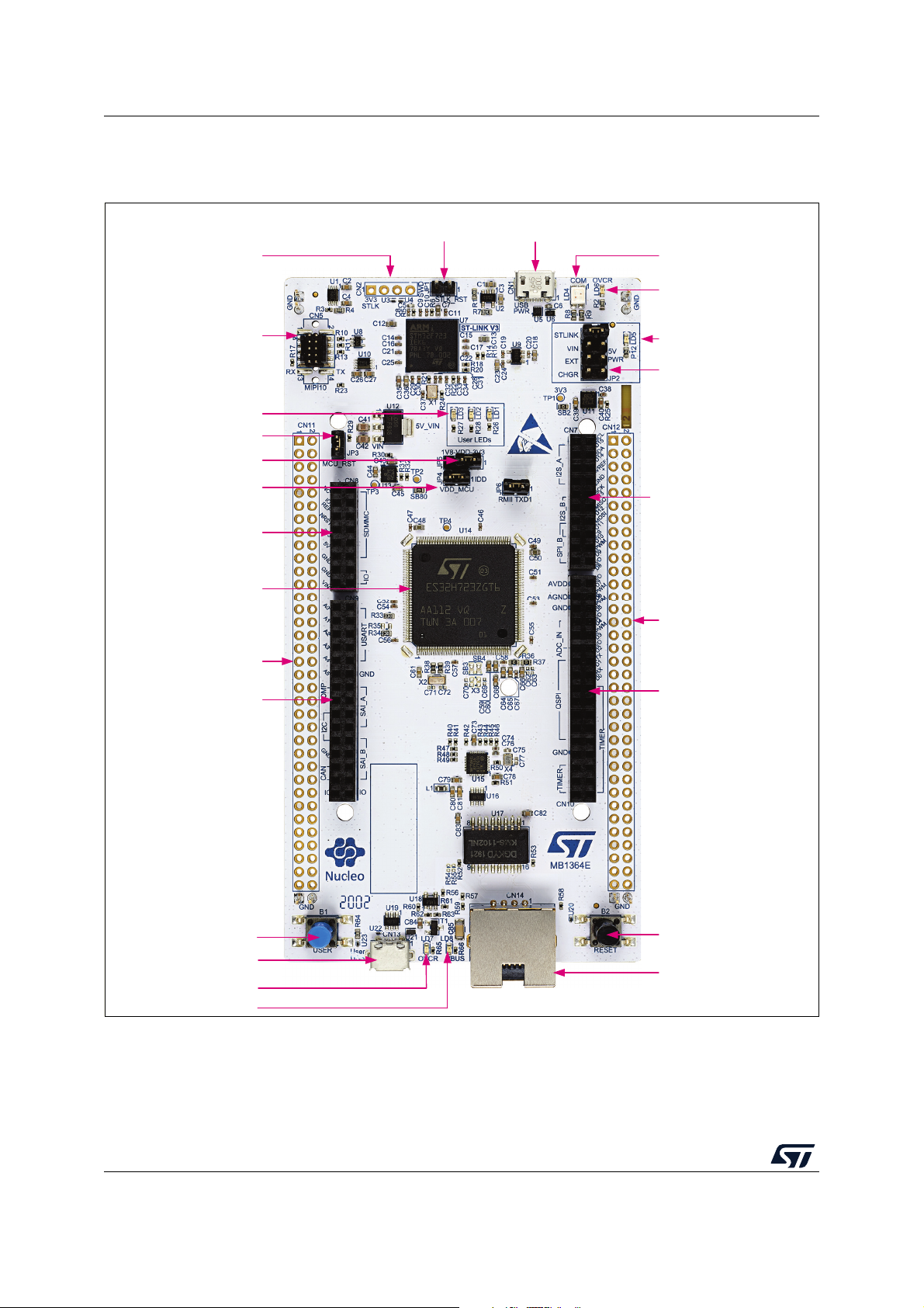
MSv62197V2
JP1 ST-LINK RST
CN13 user USB
connector
CN1 ST-LINK micro USB connector
LD6 ST-LINK
overcurrent LED (red)
LD4 COM LED (red/green)
LD5 Power LED (green)
JP2 Power source
selection
CN7 ZIO connector
CN12 ST morpho
pin header
CN10 ZIO connector
B2 reset button
CN14 Ethernet RJ45
connector
CN2 DFU connector
B1 user button
LD7 USB overcurrent LED
LD8 USB VBUS LED
CN9 ZIO connector
CN11 ST morpho
pin header
U14 STM32
microcontroller
CN8 ZIO connector
JP5 VDD_MCU
Power selection
JP4 IDD measurement
JP3 MCU RST
LD1-LD3 user LEDs
CN5 MIPI connector
6.1 Nucleo-144 board layout
Figure 4. Nucleo-144 board top layout
12/50 UM2407 Rev 2
Page 13
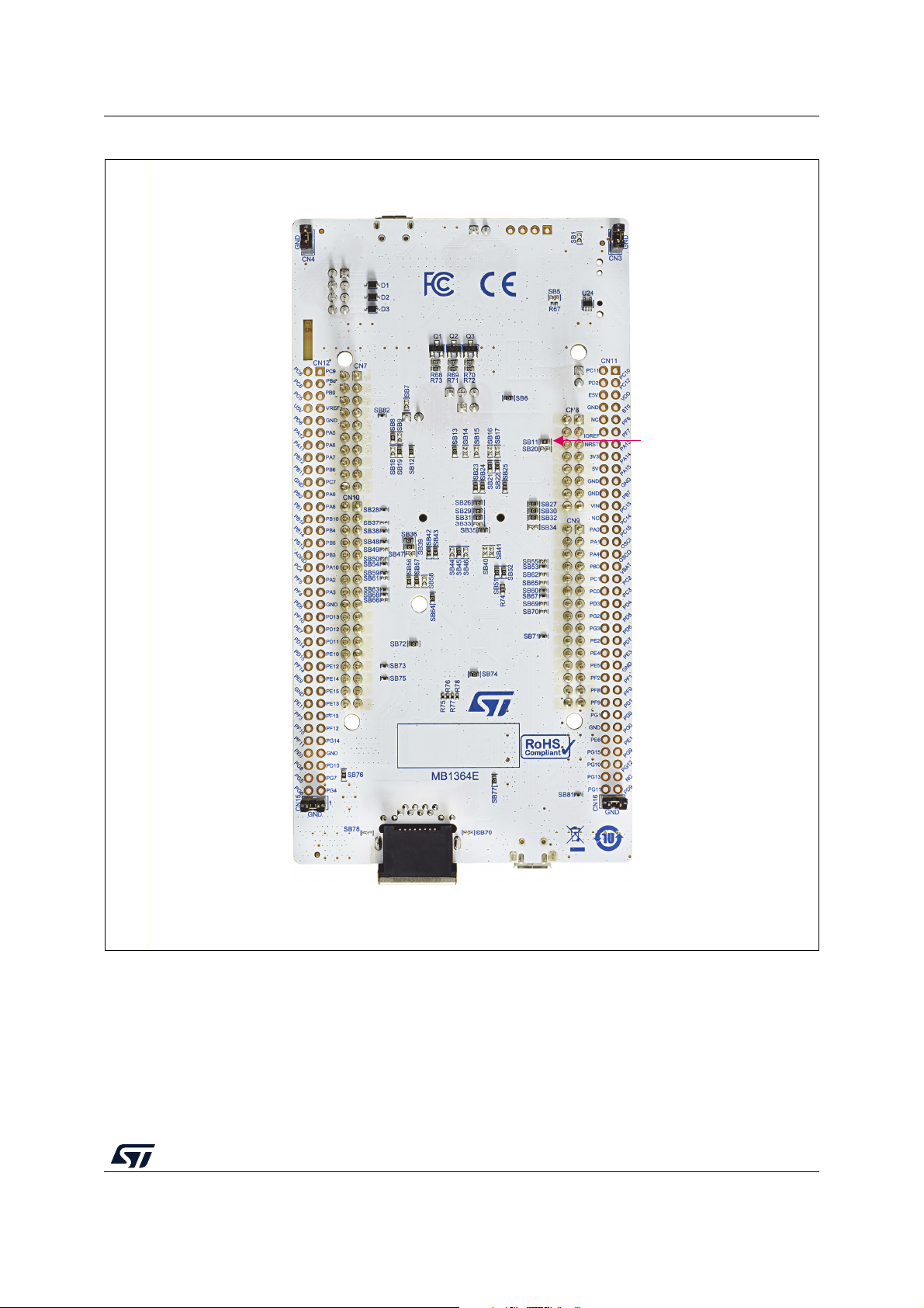
UM2407 Hardware layout and configuration
MSv51398V2
SB10, SB11, SB20
IOREF Power selection
Figure 5. Nucleo-144 bottom layout
UM2407 Rev 2 13/50
49
Page 14
Hardware layout and configuration UM2407
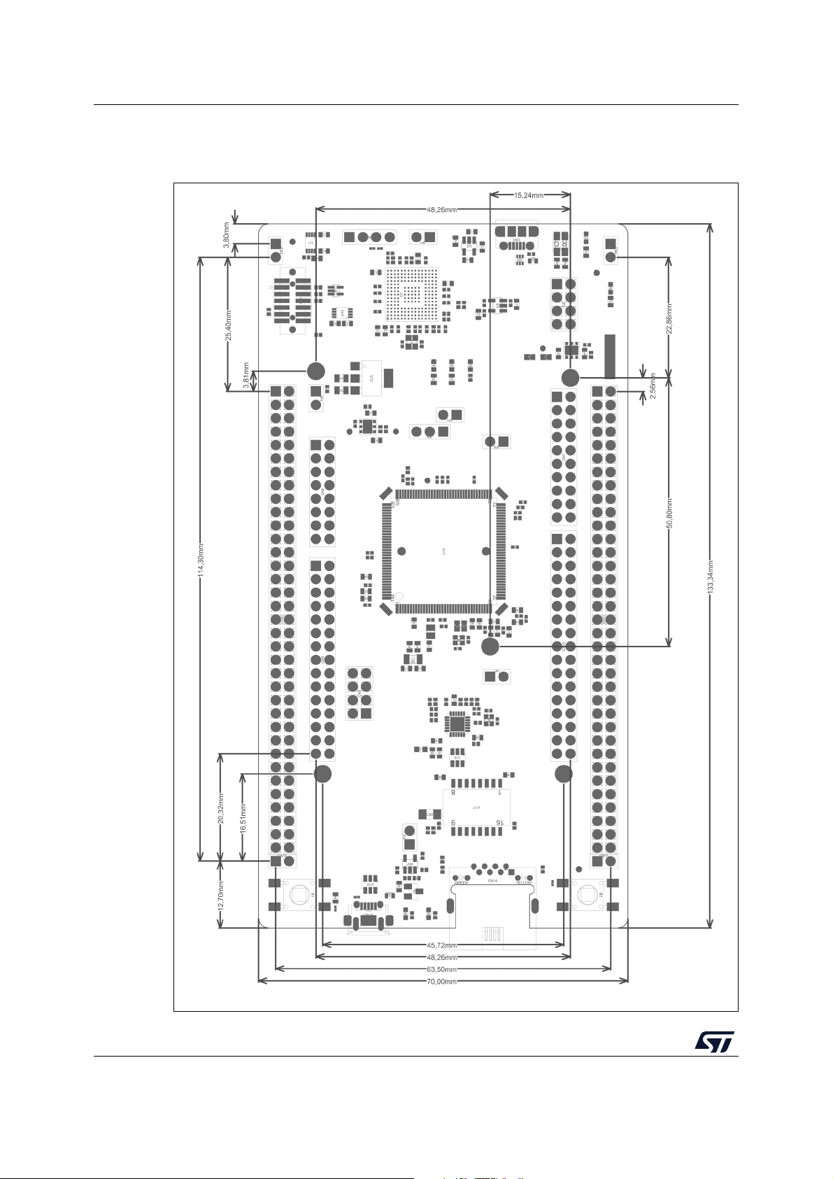
6.2 Mechanical drawing
Figure 6. Nucleo-144 board mechanical drawing in millimeter
14/50 UM2407 Rev 2
Page 15
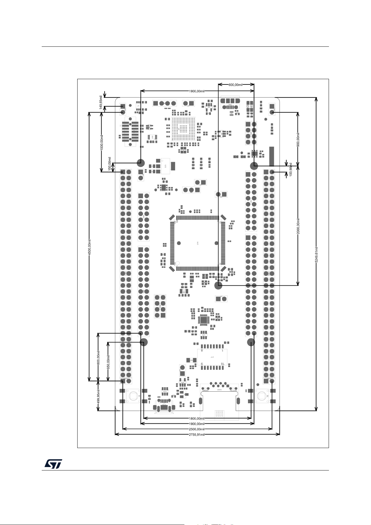
UM2407 Hardware layout and configuration
Figure 7. Nucleo-144 board mechanical drawing in mil
UM2407 Rev 2 15/50
49
Page 16

Hardware layout and configuration UM2407
6.3 Embedded STLINK-V3E
There are two different ways to program or debug the on-board STM32H7 MCU:
• Using the embedded STLINK-V3E
• Using an external debug tool connected to the CN5 MIPI-10 connector.
The STLINK-V3E programming and debugging tool is integrated into the STM32H7
Nucleo-144 board.
The STLINK-V3E makes the STM32H7 Nucleo-144 board Mbed enable.
The embedded STLINK-V3E supports only SWD and VCP for STM32H7 devices. For
information about debugging and programming features, refer to Overview of ST-LINK
derivatives, Technical note (TN1235), which describes in detail all the STLINK/V3 features.
Features supported on STLINK--V3E:
• 5 V power supplied by USB connector (CN1)
• USB 2.0 high-speed-compatible interface
• JTAG/serial wire debugging (SWD) specific features:
– 3 V to 3.6 V application voltage on the JTAG/SWD interface and 5V tolerant inputs
–JTAG
– SWD and serial viewer (SWV) communication
• Direct firmware update feature (DFU) (CN2)
• STDC14 (MIPI10) compatible connector (CN5)
• Status COM LED (LD4) which blinks during communication with the PC
• Fault red LED (LD6) alerting on USB overcurrent request
• 5 V/300 mA output power supply capability (U2) with current limitation and LED
• Green LED ON: 5V enabled (LD5)
6.3.1 Drivers
Before connecting the Nucleo-144 board to a Windows® 7 or Windows® 8 PC via USB, a
driver for STLINK-V3E must be installed (not required for Windows
automatically installed by the toolset supporting ST-LINK. It is also available from the
www.st.com website.
In case the STM32H7 Nucleo-144 board is connected to the PC before installing the driver,
the PC device manager may report some Nucleo interfaces as “Unknown”.
To recover from this situation, after installing the dedicated driver, the association of
“Unknown” USB devices found on the STM32H7 Nucleo-144 board to this dedicated driver,
must be updated in the device manager manually.
Note: It is recommended to proceed using a USB composite device, as shown in Figure 8.
16/50 UM2407 Rev 2
®
10). The driver is
Page 17

UM2407 Hardware layout and configuration
37xx
Figure 8. USB composite device
Note: 37xx = 374E for STLINK-V3E without bridges functions
374F for STLINK-V3E with bridges functions
6.3.2 STLINK-V3E firmware upgrade
The STLINK-V3E embeds a firmware upgrade mechanism for an in-situ upgrade through
the USB port. As the firmware may evolve during the lifetime of the STLINK-V3E product
(for example new functionalities, bug fixes, support for new microcontroller families), it is
recommended to keep the STLINK-V3E firmware up to date before starting to use the
STM32H7 Nucleo-144 board. The latest version of this firmware is available from the
www.st.com website.
6.3.3 Using an external debug tool to program and debug the on-boards STM32H7
There are two basic ways to support an external debug tool:
1. Keep the embedded STLINK-V3E running.
Power on the STLINK-V3E at first until the COM LED lights RED. Then connect your
external debug tool through CN5 MIPI-10 debug connector.
2. Set the embedded STLINK-V3E in the high-impedance state:
When you state the jumper JP1 (STLK_RST) ON, the embedded STLINK-V3E is in
RESET state and all GPIOs are in high impedance, then you can connect your external
Debug tool on the debug connector CN5.
UM2407 Rev 2 17/50
49
Page 18

Hardware layout and configuration UM2407
MSv61202V2
Power supply selection
STLINK-V3E USB connector
JP1 STLK_RST
External debug tool
Figure 9. Connecting an external debug tool to program the on-board STM32H7
MIPI-10
Pin
STDC14
Pin
Table 5. MIPI-10 debug connector (CN5)
CN5 Designation
-1NCReserved
-2NCReserved
13 T_VCCTarget VCC
24 T_SWDIO
Target SWDIO using SWD protocol or Target JTMS
(T_JTMS) using JTAG protocol
35 GNDGround
46 T_SWCLK
Target SWCLK using SWD protocol or Target JCLK (T_JCLK)
using JTAG protocol
57 GNDGround
68 T_SWO
7 9 T_JRCLK
8 10 T_JTDI
9 11 GNDDetect
Target SWO using SWD protocol or Target JTDO (T_JTMS)
using JTAG protocol
Not used by SWD protocol, Target JRCLK (T_JRCLK) using
JTAG protocol, only for specific use
Not used by SWD protocol, Target JTDI (T_JTDI) using JTAG
protocol, only for external tools
GND detect for plug indicator, used on SWD and JTAG
neither
10 12 T_NRST
Target NRST using SWD protocol or Target JTMS (T_JTMS)
using JTAG protocol
18/50 UM2407 Rev 2
Page 19

UM2407 Hardware layout and configuration
Table 5. MIPI-10 debug connector (CN5) (continued)
MIPI-10
Pin
-13T_VCP_RX
-14T_VCP_TX
STDC14
Pin
6.4 Power supply
The power supply can be provided by five different sources:
• A host PC connected to CN1 through a USB cable (default setting)
• An external 7 V to 12 V power supply connected to CN8 pin 15 or CN11 pin 24
• An external 5 V power supply connected to CN11 pin 6
• An external 5 V USB charger (5V_USB_CHGR) connected to CN1
• An external 3.3 V power supply (3V3) connected to CN8 pin 7 or CN11 pin 16
The power supply is provided either by the host PC through the USB cable or by an external
source: V
V
, E5V, or +3.3 V is used to power the Nucleo-144 board, this power source must comply
IN
with the standard EN-60950-1: 2006+A11/2009 and must be Safety Extra Low Voltage
(SELV) with limited power capability.
(7 V to 12 V), E5V (5 V), or +3.3 V power supply pins on CN8 or CN11. In case
IN
CN5 Designation
Target RX used for VCP (must be UART dedicated to
bootloader)
Target TX used for VCP (must be UART dedicated to
bootloader)
In case the power supply is +3.3 V, the STLINK-V3E is not powered and cannot be used.
6.4.1 Power supply input from STLINK-V3E USB connector (default setting)
The STM32H7 Nucleo-144 board and shield can be powered from the STLINK-V3E USB
connector CN1 (5
Figure 10).
This is the default setting.
V), by placing a jumper between the pins 1-2 of JP2 ‘STLINK’ (Refer to
UM2407 Rev 2 19/50
49
Page 20

Hardware layout and configuration UM2407
MSv61203V2
U7
STM32F723
STLINK-V3
CN1
U2
5V
3V3
PC
3V3
Figure 10. Power supply input from STLINK-V3E USB connector with PC (5 V, 500 mA max)
If the USB enumeration succeeds, the 5V_ST_LINK power is enabled, by asserting the
PWR_ENn signal from STM32F723IEK6 ‘STLINK-V3E’ (U7). This pin is connected to a
power switch STMPS2151STR (U2), which powers the board. The power switch
STMPS2151STR (U2) features also a current limitation to protect the PC in case of shortcircuit onboard. If an overcurrent (more than 500
mA) happens onboard, the red LED LD6 is
lit.
Nucleo board and its shield on it can be powered from STLINK-V3E USB connector CN1,
but only the STLINK-V3E circuit gets power before USB enumeration because the host PC
only provides 100
mA to the board at that time.
During the USB enumeration, the Nucleo board asks for the 500 mA power to the host PC.
• If the host is able to provide the required power, the enumeration finishes by a
SetConfiguration command and then, the power switch STMPS2151STR is switched
ON, the Green LED LD5 is turned ON, thus Nucleo board and its shield on it can
consume 500 mA current, but no more.
• If the host is not able to provide the requested current, the enumeration fails.
Therefore, the STMPS2151STR power switch (U2) remains OFF and the MCU part
including the extension board is not powered. As a consequence, the GREEN LED
LD5 remains turned OFF. In this case, it is mandatory to use an external power supply.
Warning: In case the maximum current consumption of the
STM32H7 Nucleo-144 board and its shield boards exceed
300 mA, it is mandatory to power the STM32H7 Nucleo-144
board, using an external power supply connected to E5V, V
or +3.3 V.
6.4.2 External power supply input from VIN (7 V to 12 V, 800 mA max)
IN
When STM32H7 Nucleo-144 board is power supplied by VIN (Refer to Tab le 6 and
Figure 11), the jumper configuration must be the following: Jumper JP2 on pin 3-4 ‘VIN’
20/50 UM2407 Rev 2
Page 21

UM2407 Hardware layout and configuration
MSv61204V2
MSv61203V1
CN1
U2
3V3
3V3
The Nucleo-144 board and its shield boards can be powered in three different ways from an
external power supply, depending on the voltage used. The three power sources are
summarized in
Table 6.
Table 6. External power sources: VIN (7 V to 12 V)
Input power
name
V
IN
Connector pins Voltage range Max current Limitation
From 7 V to 12 V only and input current
capability is linked to input voltage:
CN8 pin 15 CN11
pin 24
7 V to 12 V 800 mA
– 800 mA input current when V
– 450 mA input current when 7 V<VIN<9 V
– 250 mA input current when 9 V<V
Figure 11. Power supply input from VIN (7 V to 12 V, 800 mA max)
IN
=7 V
<12 V
IN
Note: Refer to Section 6.4.6 about debugging when using an external power supply.
6.4.3 External power supply input 5V_EXT (5 V, 500 mA max)
When STM32H7 Nucleo-144 board is power supplied by EXT (Refer to Table 7 and
Figure 12), the jumper configuration must be the following: Jumper JP2 on pin 5-6 ‘EXT’
Input power name Connector pins Voltage range Max current
EXT CN11 pin 6 4.75 V to 5.25 V 500 mA
Note: Refer to Section 6.4.6 about debugging when using an external power supply.
Table 7. External power sources: 5V_EXT
UM2407 Rev 2 21/50
49
Page 22
Hardware layout and configuration UM2407
MSv61205V2
U2
5V_EXT
3V3
3V3
MSv61206V2
NO DEBUG
CN1
5V
3V3
USB CHARGER
3V3
Figure 12. Power supply input from 5V_EXT (5 V, 500 mA max)
6.4.4 External power supply input from USB CHARGER (5 V)
When STM32H7 Nucleo-144 board is power supplied by a USB charger on CN1 (Refer to
Table
8 and Tabl e 13), the jumper configuration must be the following: Jumper JP2 on
pin 7-8 ‘CHGR’.
Table 8. External power sources: CHGR (5 V)
Input power name Connector pins Voltage range Max current
CHGR CN1 5 V -
Figure 13. Power supply input from STLINK-V3E USB connector with a USB charger (5 V)
6.4.5 External power supply input from 3V3_EXT (3.3 V)
When the 3.3 V is provided by a shield board, it is interesting to use the 3V3 (CN8 pin 7 or
CN11 pin 16) directly as power input (Refer to
programming and debugging features are not available, since the STLINK-V3E is not
powered.
Table 9 and Figure 14). In this case,
22/50 UM2407 Rev 2
Page 23

UM2407 Hardware layout and configuration
MSv61207V2
MSv61203V1
CN1
U2
3V3
NO DEBUG
3V3
NO JUMPER
Table 9. External power sources: 3V3_EXT (3.3 V)
Input power name Connector pins Voltage range Max current
3V3
CN8 pin 7
CN11 pin 16
3 V to 3.6 V 1.3 A
Figure 14. Power supply input from 3V3_EXT (3.3 V)
6.4.6 Debugging while using VIN or EXT as an external power supply
When powered by VIN or EXT, it is still possible to use the STLINK-V3E for programming or
debugging only, but it is mandatory to power the board first using VIN or EXT, then to
connect the USB cable to the PC. In this way, the enumeration succeeds, thanks to the
external power source.
The following power-sequence procedure must be respected:
1. Connect jumper JP2 between pin 5 and pin 6 for EXT or between pin 3 and pin 4 for
VIN
2. Connect the external power source to VIN or EXT
3. Power on the external power supply 7 V< VIN < 12 V to VIN, or 5 V for EXT
4. Check that the green LED LD5 is turned ON
5. Connect the PC to the USB connector CN1
If this order is not respected, the board may be powered by USB (U5V) first, then by VIN or
EXT as the following risks may be encountered:
1. If more than 300 mA current is needed by the board, the PC may be damaged or the
current supplied can be limited by the PC. As a consequence, the board is not powered
correctly.
2. 300 mA is requested at enumeration so there is a risk that the request is rejected and
the enumeration does not succeed if the PC cannot provide such current.
Consequently, the board is not power supplied (LED LD5 remains OFF).
UM2407 Rev 2 23/50
49
Page 24
Hardware layout and configuration UM2407
6.5 Clock sources
6.5.1 HSE clock (high-speed external clock)
There are four ways to configure the pins corresponding to the external high-speed clock
(HSE):
• MCO from STLINK-V3E (default): MCO output of ST-LINK is used as an input clock.
This frequency cannot be changed, it is fixed at 8 MHz and connected to the PF0/PH0OSC_IN of STM32H7 Series microcontroller. The configuration must be:
– SB44 and SB46 OFF
–SB45 ON
– SB3 and SB4 OFF
• HSE on-board oscillator from X3 crystal (not provided): for typical frequencies and its
capacitors and resistors, refer to the STM32H7 Series microcontroller datasheet and to
the Oscillator design guide for STM8AF/AL/S and STM32 microcontrollers Application
note (AN2867) for the oscillator design guide. The X3 crystal has the following
characteristics: 25 MHz, 6 pF, 20 ppm. It is recommended to use
NX2016SA-25MHz-EXS00A-CS11321 manufactured by NDK. The configuration must
be:
– SB44 and SB46 OFF
– SB3 and SB4 ON
– C69 and C70 soldered with 5.6 pF capacitors
–SB45 OFF
Oscillator from external PF0/PH0: from an external oscillator through the pin 29 of the CN11
connector. The configuration must be:
–SB46 ON
–SB45 OFF
– SB3 and SB4 OFF
• HSE not used: PF0/PH0 and PF1/PH1 are used as GPIOs instead of clocks. The
configuration must be:
– SB44 and SB46 ON
–SB45 OFF
– SB3 and SB4 OFF
6.5.2 LSE clock (low-speed external clock) - 32.768 kHz
There are three ways to configure the pins corresponding to the low-speed clock (LSE):
• On-board oscillator (default): X2 crystal. Refer to the Oscillator design guide for
STM8AF/AL/S and STM32 microcontrollers Application note (AN2867) for oscillator
design guide for STM32H7 Series microcontrollers. It is recommended to use
24/50 UM2407 Rev 2
Page 25

UM2407 Hardware layout and configuration
NX3215SA-32.768kHZ-EXS00A-MU00525 (32.768 kHz, 6 pf load capacitance,
20 ppm) from NDK. The configuration must be:
– SB40 and SB41 OFF
– R38 and R39 ON
• Oscillator from external PC14: from external oscillator through the pin 25 of CN11
connector. The configuration must be:
– SB40 and SB41 ON
– R38 and R39 OFF
• LSE not used: PC14 and PC15 are used as GPIOs instead of the low-speed clock.
The configuration must be:
– SB40 and SB41 ON
– R38 and R39 OFF
6.6 Board functions
6.6.1 LEDs
User LD1: a green user LED is connected to the STM32H7 I/O PB0 (SB39 ON and SB47
OFF) or PA5 (SB47 ON and SB39 OFF) corresponding to the ST Zio D13.
User LD2: a yellow user LED is connected to PE1.
User LD3: a red user LED is connected to PB14.
These user LEDs are on when the I/O is HIGH value, and are off when the I/O is LOW.
LD4 COM: the tricolor LED LD4 (green, orange, red) provides information about ST-LINK
communication status. LD4 default color is red. LD4 turns to green to indicate that
communication is in progress between the PC and the STLINK-V3E, with the following
setup:
• Slow blinking red/OFF at power-on before USB initialization
• Fast blinking red/OFF after the first correct communication between PC and
STLINK-V3E (enumeration)
• Red LED ON when the initialization between the PC and STLINK-V3E is complete
• Green LED ON after a successful target communication initialization
• Blinking red/green during communication with the target
• Green ON communication finished and successful
• Orange ON communication failure
LD5 PWR: the green LED indicates that the STM32H7 part is powered and +5 V power is
available on CN8 pin 9 and CN11 pin 18.
LD6 USB power fault: LD5 indicates that the board power consumption on USB exceeds
500
mA, consequently the user must power the board using an external power supply.
LD7 and LD8 USB FS: Refer to Section 6.6.6: USB OTG FS.
UM2407 Rev 2 25/50
49
Page 26
Hardware layout and configuration UM2407
6.6.2 Push-buttons
B1 USER (blue button): the user button is connected to the I/O PC13 by default (tamper
support: SB51 ON and SB58 OFF) or PA0 (Wakeup support: SB58 ON and SB51 OFF) of
the STM32H7 Series microcontroller.
B2 RESET (black button): this push-button is connected to NRST and is used to reset the
STM32H7 Series microcontroller.
6.6.3 MCU voltage selection: 1V8/3V3
The STM32H7 Nucleo-144 board offers the possibility to supply the STM32H7 Series
microcontroller with 1.8
• Place the JP5 jumper on 3V3 to supply the MCU with 3V3, connecting pins 1 and 2.
• Place the JP5 jumper on 1V8 to supply the MCU with 1V8, connecting pins 2 and 3.
V or 3.3 V. JP5 is used to select the VDD_MCU power level.
6.6.4 Current consumption measurement (IDD)
Jumper JP4, labeled IDD, is used to measure the STM32H7 Series microcontroller
consumption by removing the jumper and by connecting an ammeter:
• JP4 must be ON when STM32H7 is powered with 3V3_VDD (default)
• If JP4 is OFF, an ammeter must be connected to measure the STM32H7 current. If
there is no ammeter, the STM32H7 is not powered.
Warning: on MB1364 REV.C, ‘VDD_MCU’ is also supplying Ethernet
PHY (U15) and debug voltage translation (U1 and U10).
If needed, for low power measurement (for example standby mode), in order to measure
only MCU (U7) power consumption, the user must remove the following components: R4,
R43, R44, R45, R46, R47, R48, R49, R50, R51, R52, R53, R59, R61, U1, U10, U15, and
SB45.
After removing these components, it becomes impossible to use Ethernet, and 1.8 V debug
with STLINK-V3E.
6.6.5 Virtual COM port (VCP): LPUART/USART
The STM32H7 Nucleo-144 board offers the possibility to connect an LPUART or a USART
interface to the STLINK-V3E or to the ST morpho connectors and ARDUINO
connectors.
The selection is done by settings the related solder bridges. (Refer to Tab le 10 and Table 11
below).
By default the USART3 communication between the target STM32H7 and the STLINK-V3E
is enabled, to support the Virtual COM port for the Mbed (SB5 and SB6 ON).
®
Uno V3
26/50 UM2407 Rev 2
Page 27

UM2407 Hardware layout and configuration
Pin
name
PD8 USART3 TX SB5 ON and SB7 OFF SB5 OFF and SB7 ON
PD9 USART3 RX SB6 ON and SB4 OFF SB6 OFF and SB4 ON
Pin
name
PB6 LPUART1 TX
PB7 LPUART1 RX
Function
Function Virtual COM port
Table 10. USART3 connection
Virtual COM port
(default configuration)
Table 11. LPUART1 connection
ARDUINO
SB9 ON
SB8 and SB18 OFF
SB34 ON
SB12 and SB68 OFF
SB8 ON
SB9 and SB18 OFF
SB68 ON
SB34 and SB66 OFF
ST morpho connection
®
D0 and
D1
ST morpho connection
SB9 OFF and SB18 OFF
SB12 OFF and SB34
OFF
Hardware connection required for USART bootloader:
The STM32H7x3 embeds a USART bootloader. To use the USART bootloader (USART1),
hardware modifications are required on the NUCLEO board. Flying wires have to be
connected between PD8/PD9 (USART3 available on SB19/SB12) and PB10/PB11
(USART1 available on CN15).
6.6.6 USB OTG FS
The STM32H7 Nucleo-144 board supports USB OTG FS communication via a USB MicroAB connector (CN13) and USB power switch (U18) connected to V
Warning: USB Micro-AB connector (CN13) cannot power the Nucleo-
144 board. To avoid damaging the STM32H7, it is mandatory
to power the Nucleo-144 before connecting a USB cable on
CN13. Otherwise, there is a risk of current injection on
STM32H7 I/Os.
A green LED LD8 lights in one of these cases:
• Power switch (U12) is ON and STM32H7 Nucleo-144 board works as a USB host
• V
is powered by another USB host when the STM32H7 Nucleo-144 board works as
BUS
a USB device.
The red LED LD7 lights if overcurrent occurs when +5 V is enabled on V
mode.
Note: 1.It is recommended to power the Nucleo-144 board with an external power supply when
using USB OTG or host function.
2.SB76 must be ON when using USB OTG FS.
BUS
.
in USB host
BUS
UM2407 Rev 2 27/50
49
Page 28

Hardware layout and configuration UM2407
Pin
name
PA8 USB SOF - - Test point TP4
PA9 USB V
PA10 USB ID SB24 ON SB24 OFF -
PA11 USB DM SB21 ON SB21 OFF -
PA12 USB DP SB22 ON SB22 OFF -
PD10 USB PWR EN SB77 ON SB77 OFF -
PG7 USB FS OVCR SB76 ON SB76 OFF -
ESD protection part USBLC6-2SC6 is implemented on USB port because all USB pins on
STM32H7 are dedicated to USB port protection only on the STM32H7 Nucleo-144 board.
USB pin ID is not used.
6.6.7 Ethernet
The STM32H7 Nucleo-144 board supports 10M/100M Ethernet communication by a PHY
LAN8742A-CZ-TR (U15) and RJ45 connector (CN14). Ethernet PHY is connected to the
STM32H7 Series microcontroller via the RMII interface. 50
Series microcontroller is generated by the PHY RMII_REF_CLK.
Function
BUS
Table 12. USB pin configuration
Configuration
when using USB
connector
SB23 ON SB23 OFF -
Configuration
when using ST
morpho connector
MHz clock for the STM32H7
Remark
Note: 1.JP6 and SB72 must be ON when using Ethernet.
2.Ethernet PHY LAN8742A must be set in power-down mode (in this mode Ethernet PHY
ref clock turns off) to achieve the expected low-power mode current. This is done by
configuring Ethernet PHY LAN8742A basic control register (at address 0x00) bit 11 (power
down) to '1'. SB57 can also be OFF to get the same effect.
Pin
name
PA1
PA2 RMII MDIO - SB72 ON SB72 OFF
PC1 RMII MDC - SB64 ON SB64 OFF
PA7 RMII RX Data Valid - SB31 ON SB31 OFF
PC4 RMII RXD0 - SB36 ON SB36 OFF
PC5 RMII RXD1 - SB29 ON SB29 OFF
PG11 RMII TX Enable - SB27 ON SB27 OFF
PG13 RXII TXD0 - SB30 ON SB30 OFF
PB13 RMII TXD1 I2S_A_CK JP6 ON JP6 OFF
Function
RMII Reference
Clock
Table 13. Ethernet pin configuration
Conflict with
ST Zio
connector
signal
- SB57 ON SB57 OFF
Configuration when
using Ethernet
Configuration when
using
ST Zio or ST morpho
connector
28/50 UM2407 Rev 2
Page 29

UM2407 Hardware layout and configuration
6.7 Solder bridges and jumpers
SBxx can be found on the top layer and SB1xx can be found on the bottom layer of the
Nucleo-144 board.
Bridge State
Table 14. Solder bridge and jumper configuration
(1)
Description
SB1 (3V3_PER)
SB2 (3V3)
SB80 (1V8_VDD)
SB6
SB12, SB19 (ST-LINKUSART)
JP1 (ST-LINK_RST)
SB32
(SWO)
ON Peripheral power 3V3_PER is connected to 3V3.
OFF Peripheral power 3V3_PER is not connected.
ON
OFF
ON
Output of voltage regulator ST1L05CPU33R is connected to
3V3.
Output of voltage regulator ST1L05CPU33R is not
connected.
Output of voltage regulator ST1L05BPUR is connected to
1V8_VDD.
OFF Output of voltage regulator ST1L05BPUR is not connected.
ON
Input of voltage regulator ST1L05BPUR is connected to
3V3_VDD.
OFF Input of voltage regulator ST1L05BPUR is not connected.
PG9 and PG14 on ST-LINK STM32F723IEK6 are connected
ON
to PD8 and PD9 to enable virtual COM port for Mbed support.
Thus PD8 and PD9 on the ST morpho connectors cannot be
used.
OFF
PG9 and PG14 on ST-LINK STM32F723IEK6 are
disconnected to PD8 and PD9 on STM32H7.
OFF No incidence on ST-LINK STM32F723IEK6 NRST signal.
ON
ST-LINK STM32F723IEK6 signal is connected to GND
(ST-LINK reset to reduce power consumption).
SWO signal of the STM32H7 (PB3) is connected to ST-LINK
ON
SWO input.
(SB26 must be removed)
OFF SWO signal of STM32H7 is not connected.
JP3
(NRST)
SB10, SB11, SB20
(IOREF)
ON
OFF
OFF, ON,
OFF
ON, OFF,
OFF
OFF, OFF,
ON
Board RESET signal (NRST) is connected to ST-LINK reset
control I/O (T_NRST).
Board RESET signal (NRST) is not connected to ST-LINK
reset control I/O (T_NRST).
IOREF is connected to VDD_MCU.
IOREF is connected to 3V3_PER.
IOREF is connected to 3V3.
UM2407 Rev 2 29/50
49
Page 30

Hardware layout and configuration UM2407
Table 14. Solder bridge and jumper configuration (continued)
Bridge State
(1)
Description
SB14 (SDMMC_D0),
SB15 (SDMMC_D1)
SB39, SB47
(LD1-LED)
SB33, SB35
(D11)
SB40,SB41
(X2 crystal)
SB44 (PF1/PH1)
SB46 (PF0/PH0)
(Main clock)
ON These pins are connected to ST morpho connector CN12.
OFF
These pins are disconnected from ST morpho connector
CN12 to avoid stub of SDMMC data signals on PCB.
ON, OFF Green user LED LD1 is connected to PB0.
OFF, ON
Green user LED LD1 is connected to D13 of ARDUINO
signal (PA5).
®
OFF, OFF Green user LED LD1 is not connected.
ON, ON Forbidden
OFF, ON
ON, OFF
D11 (Pin 14 of CN7) is connected to STM32H7 PB5
(SPI_A_MOSI/ TIM_D_PWM2)
D11 (Pin 14 of CN7) is connected to STM32H7 PA7
(SPI_A_MOSI/ TIM_E_PWM1)
PC14, PC15 are not connected to ST morpho connector
OFF, OFF
CN11.
(X2 used to generate 32 kHz clock).
ON, ON
PC14, PC15 are connected to ST morpho connector CN11.
(R38 and R39 must be removed).
PF0/PH0 is not connected to ST morpho connector CN11
ON, OFF
PF1/PH1 is connected to ST morpho connector CN11
(MCO is used as the main clock for STM32H7 on PF0/PH0 –
SB45 ON).
PF0/PH0, PF1/PH1 are not connected to ST morpho
OFF, OFF
connector CN11
(X3, C69, C70, SB3, and SB4 provide a clock. In this case,
SB45 must be removed).
PF0/PH0 and PF1/PH1 are connected to ST morpho
ON, ON
connector CN11.
(SB3, SB4, and SB45 must be removed).
MCO of ST-LINK (STM32F723IEK6) is connected to
PF0/PH0 of STM32H7.
MCO of ST-LINK (STM32F723IEK6) is not connected to
PF0/PH0 of STM32H7.
PF0/PH0 and PF1/PH1 are not connected to external
25 MHz crystal X3.
PF0/PH0 and PF1/PH1 are connected to external 25 MHz
crystal X3.
pin of STM32H7 is connected to V
BAT
pin of STM32H7 is not connected to V
BAT
SB45
(STLK_MCO)
SB3, SB4
(external 25M crystal)
SB52
)
(V
BAT
ON
OFF
OFF, OFF
ON, ON
ON V
OFF V
30/50 UM2407 Rev 2
DD_MCU
DD_MCU
.
.
Page 31

UM2407 Hardware layout and configuration
Table 14. Solder bridge and jumper configuration (continued)
Bridge State
SB51, SB58
(B1-USER)
ON, OFF B1 push-button is connected to PC13.
OFF, ON
OFF, OFF B1 push-button is not connected.
(1)
Description
B1 push-button is connected to PA0 (Set SB51 OFF if the ST
Zio connector is used).
SB75
(PA0)
RMII Signals
SB57 (PA1), SB64
(PC1),
SB72 (PA2), SB36
(PC4),
SB29 (PC5), SB30
(PG13), SB27 (PG11),
SB31 (PA7), JP6
(PB13)
SB74 (Ethernet nRST)
RMII Signal
SB76 (PG7)
SB77 (PD10)
SB23 (PA9)
SB24 (PA10)
SB21 (PA11), SB22
(PA12)
SB13
ON PA0 is connected to the ST Zio connector (Pin 29 of CN10).
OFF
PA0 is not connected to the ST Zio connector (Pin 29 of
CN10).
These pins are used as RMII signals and connected to
Ethernet PHY.
ON
(SB7 must be removed)
These pins must not be used on the ST morpho or the ST Zio
connectors.
These pins can be used as GPIOs on the ST morpho
OFF
connectors.
PB13 can be used as I2S_A_CK on ST Zio (Pin 5 of CN7) if
not used on the ST morpho.
ON NRST of STM32H7 is connected to Ethernet PHY (U15).
OFF NRST of STM32H7 is not connected to Ethernet PHY (U15).
ON USB overcurrent alarm is connected.
OFF
ON
USB overcurrent alarm is not connected. PG7 is used as
GPIO on the ST morpho connector (CN12).
PD10 is connected to Enable for Power switch (U18) to
control V
BUS
.
OFF PD10 is used as GPIO on the ST morpho connector (CN12).
ON PA9 is connected to USB V
OFF
PA9 is not connected to USB V
PA9 is used as GPIO on the ST morpho connector (CN12).
BUS
.
BUS
.
ON PA10 is connected to USB ID.
OFF
ON
OFF
PA10 is not connected to USB ID.
PA10 is used as GPIO on the ST morpho connector (CN12).
These pins are used as D- and D+ on USB connector CN13.
(SB16 and SB17 must be OFF).
These pins are used as GPIOs on the ST morpho
connectors.
ON VDD33_USB_1 is connected to 3V3_VDD.
OFF VDD33_USB_1 is not supplied.
SB25
ON VDD_MMC_1 is connected to VDD_MCU.
OFF VDD_MMC_1 is not supplied.
UM2407 Rev 2 31/50
49
Page 32

Hardware layout and configuration UM2407
Table 14. Solder bridge and jumper configuration (continued)
Bridge State
(1)
Description
SB59 (PG6)
ON PG6 is connected to QSPI_CS (SB61 must be OFF).
OFF PG6 is used as GPIO on the ST morpho connector (CN12).
ON PB2 is connected to QSPI_CLK. (SB69 must be OFF)
SB63 (PB2)
OFF
SB71, SB73
(PE6)
ON, OFF PE6 is connected to SAI_A_SD (D59 of CN9)
OFF, ON PE6 is connected to TIMER_A_BKIN2 (D38 of CN10)
ON
SB67 (PE2)
OFF PE2 is used as QSPI_BK1_IO2 (D31 of CN10).
SB53 (PC2) and
SB60 (PF10)
ON
OFF
SB65 (PF11) OFF
2
C
I
ON
SB55 (PB9) and SB62
(PB8)
OFF
PB2 is not connected to QSPI_CLK and can be used as
COMP1_INP (SB69 ON) or used as GPIO on the ST morpho
connector CN12. (SB69 OFF)
PE2 is connected to SAI_A_MCLK (D56 of CN9).
QSPI_BK1_IO2 cannot be used (D31 of CN10).
ADC_IN are connected to A4 and A5 (pin 9 and 11) on the ST
Zio connector CN9. Thus SB55 and SB62 must be OFF
ADC_IN are connected to A4 and A5 (pin 9 and 11) on the ST
Zio connector CN9. Thus SB55 and SB62 can be ON (I
2
C)
On NUCLEO-H723ZG, NUCLEO-H743ZI2, and NUCLEOH753ZI, PF11 is used only as GPIO on the ST morpho
connector (CN12) and must not be used as ADC_IN.
PB9 and PB8 (I2C) are connected to A4 and A5 (pin 9 and
11) on the ST Zio connector CN9. Thus SB60 and SB53 must
be OFF
PB9 and PB8 (I2C) are not connected to A4 and A5 (pin 9
and 11) on the ST Zio connector CN9.
ON, OFF
PE9 is used as TIMER_A_PWM1 (Pin 4) on the ST Zio
connector CN10.
SB28 and SB70 (PE9)
PE9 is used as COMP2_INP (Pin 15) on the ST Zio
connector CN9.
ADC_IN is connected to A6 (pin 7) on the ST Zio connector
CN10.
PF12 must not be used as ADC_IN (SB37 must be OFF)
ADC_IN is connected to A7 (pin 9) on the ST Zio connector
CN10.
PF13 must not be used as ADC_IN (SB49 must be OFF)
ADC_IN is connected to A8 (pin 11) on the ST Zio connector
CN10.
PF14 must not be used as ADC_IN (SB50 must be OFF)
SB37 (PF12) and
SB38 (PF4)
SB48 (PF5) and SB49
(PF13)
SB50 (PF14) and
SB54 (PF6)
OFF, ON
OFF, ON
ON, OFF
OFF, ON
NUCLEO-H723ZG, NUCLEO-H743ZI2, and NUCLEO-
OFF
SB5
ON
1. The default SBx state is shown in bold.
H753ZI support 1V8 and 3V3 for VDD_MCU. Thus U10 level
shifter is needed and SB5 must be OFF.
If the MCU is supplied with 3V3, U10 can be by-passed and
SB5 can be ON.
32/50 UM2407 Rev 2
Page 33

UM2407 Hardware layout and configuration
All the other solder bridges present on the STM32H7 Nucleo-144 board are used to
configure several I/Os and power supply pins for compatibility of features and pinout with
the target STM32H7 supported.
The STM32H7 Nucleo-144 board is delivered with the solder bridges configured, according
to the target STM32H7 supported.
UM2407 Rev 2 33/50
49
Page 34

Board connectors UM2407
7 Board connectors
Several connectors are implemented on the STM32H7 Nucleo-144 board.
7.1 STLINK-V3 USB Micro-B connector CN1
The USB Micro-B connector CN1 is used to connect embedded STLINK-V3E to the PC for
programming and debugging purposes.
Figure 15. USB Micro-B connector CN1 (front view)
The related pinout for the USB STLINK-V3E connector is listed in Tabl e 15.
Connector
CN1
Pin
number
1 VBUS 5V_USB_CHGR - 5 V power
2 DM USB_DEV_HS_CN_N PB14 USB differential pair N
3 DP USB_DEV_HS_CN_P PB15 USB differential pair P
4 ID - - -
5 GND - - GND
Table 15. USB Micro-B connector pinout
Pin name Signal name
ST-LINK
MCU pin
Function
34/50 UM2407 Rev 2
Page 35

UM2407 Board connectors
7.2 USB OTG FS connector CN13
An USB OTG Full Speed communication link is available at USB Micro-AB receptacle
connector CN13. Micro-AB receptacle enables USB Host and USB Devices features.
Figure 16. USB OTG FS Micro-AB connector CN13 (front view)
The related pinout for the USB OTG FS connector is listed in Table 16.
Table 16. USB OTG FS Micro-AB connector pinout
Connector
CN13
Pin
number
1 VBUS USB_FS_VBUS PA9 5 V power
2 DM USB_FS_N PA11 USB differential pair M
3 DP USB_FS_P PA12 USB differential pair P
4 ID USB_FS_ID PA10 -
5 GND - - GND
Pin name Signal name MCU pin Function
7.3 Ethernet RJ45 connector CN14
The STM32H7 Nucleo-144 board supports 10Mbps/100Mbps Ethernet communication with
the U15 LAN8742A-CZ-TR PHY from MICROCHIP and CN14 integrated RJ45 connector.
The Ethernet PHY is connected to the MCU via the RMII interface.
The 25 MHz clock for the PHY is generated by oscillator X4. The 50 MHz clock for the MCU
(derived from the 25
MHz crystal oscillator) is provided by the RMII_REF_CLK of the PHY.
UM2407 Rev 2 35/50
49
Page 36

Board connectors UM2407
Figure 17. Ethernet RJ45 connector CN14 (front view)
1. Green LED: Ethernet traffic
2. Amber LED: Ethernet connection
The related pinout for the Ethernet connector is listed in Tab le 17.
Table 17. Ethernet connector pinout
Connector
CN14
Pin
number
Description MCU pin
Pin
number
Description MCU pin
1TX+ - 7 NC -
2TX- - 8 NC -
3 RX+ - 9 K, yellow LED -
4 NC - 10 A, yellow LED -
5 NC - 11 K, green LED -
6 RX- - 12 A, green LED -
36/50 UM2407 Rev 2
Page 37

UM2407 Extension connectors
MSv62196V2
NUCLEO-H723ZG
NUCLEO-H743ZI2
NUCLEO-H753ZI
CN7
CN10
CN8
CN9
1
3
5
7
9
11
13
15
17
19
2
4
6
8
10
12
14
16
18
20
1
3
5
7
9
11
13
15
2
4
6
8
10
12
14
16
1
3
5
7
9
11
13
15
17
19
21
23
25
27
29
2
4
6
8
10
12
14
16
18
20
22
24
26
28
30
1
3
5
7
9
11
13
15
17
19
21
23
25
27
29
31
33
2
4
6
8
10
12
14
16
18
20
22
24
26
28
30
32
34
D65
D66
D67
GND
D68
D69
D70
D71
D72
VIN
GND
GND
+5V
+3V3
RESET
IOREF
NC
A5
A4
A3
A2
A1
A0
D50
D49
D48
D47
D46
D45
D44
D43
GND
D55
D54
D53
D52
D51
D64
D63
D62
D61
D60
D59
D58
D57
D56
D34
D33
D32
GND
D31
D30
D29
D28
GND
D25
D24
D23
D22
D21
D20
D19
D18
D17
D16
D27
D26
A8
A7
A6
GND
AGND
AVDD
D8
D9
D10
D11
D12
D13
GND
AVDD
D14
D15
D0
D1
D2
D3
D4
D5
D6
D7
D35
D36
D37
D38
D39
D40
GND
D41
D42
PG0
PD1
PD0
GND
PF0
PF1
PF2
PE9
PB2
VIN
GND
GND
5V
3V3
NRST
IOREF
NC
PF10
PC2
PB1
PC3
PC0
PA3
PC8
PG3
PG2
PD2
PC12
PC11
PC10
PC9
GND
PD3
PD4
PD5
PD6
PD7
PG1
PF9
PF7
PF8
PE3
PE6
PE4
PE2
PE5
PE0
PB0
PA0
GND
PE2
PD11
PD12
PD13
GND
PB4
PA4
PB3
PB5
PC7
PA15
PB12
PB13
PB15
PC6
PB2
PG6
PF6
PF5
PF4
GND
AGND
VDDA
PF3
PD15
PD14
PB5
PA6
PA5
GND
VREFP
PB9
PB8
PB7
PB6
PG14
PE13
PE14
PE11
PE9
PG12
PB11
PB10
PE15
PE6
PE12
PE10
PE7
PE8
GND
Arduino subset of Zio = A0 to A5 and D0 to D15
Zio extension = A6 to A8 and D16 to D72
USB
OTG
USB
ST-LINK
ETHERNET
8 Extension connectors
8.1 ST Zio connectors
For all STM32H7 Nucleo-144 boards, the following figure shows the signals connected by
default to the ST Zio connectors (CN7, CN8, CN9, CN10), including the support for
ARDUINO
®
Uno V3.
Figure 18. NUCLEOH7 Nucleo-144 board
®
Uno V3. Most shields designed for ARDUINO® Uno
2
C on A4 (pin 9) and A5 (pin 11 of CN9).
UM2407 Rev 2 37/50
49
CN7, CN8, CN9, and CN10 are female on top side and male on bottom side connectors.
They include support for ARDUINO
V3 can fit the STM32H7 Nucleo-144 board.
To cope with ARDUINO® Uno V3, apply the following modifications:
• SB55 and SB62 must be ON
• SB53/60/65 must be OFF to connect I
Page 38

Extension connectors UM2407
Caution:1 The I/Os of STM32H7 Series microcontroller are 3.3 V compatible instead of 5 V for
ARDUINO
Caution:2 R37 must be removed before implementing ARDUINO
®
Uno V3.
®
shield with V
power being
REF+
provided on CN7 pin 6. Refer to Table 14: Solder bridge and jumper configuration for details
on R37.
38/50 UM2407 Rev 2
Page 39

NUCLEO-H723ZG, NUCLEO-H743ZI2, and NUCLEO-H753ZI pin assignments
UM2407 Extension connectors
Pin
Pin
name
Signal name
STM32H7
pin
Table 18. CN7 ZIO connector pinout
MCU
Function
Pin Pin name Signal name STM32H7 pin MCU Function
(1)
1D16I2S_A_MCK PC6 I2S_2 2D15 I2C_A_SCL PB8 I2C_1_SCL
3D17I2S_A_SD PB15 I2S_2 4D14 I2C_A_SDA PB9 I2C_1_SDA
5D18I2S_A_CK PB13
(2)
I2S_2 6VREFPVREFP - VDDA/VREFP
7D19I2S_A_WS PB12 I2S_2 8GND GND - -
9D20I2S_B_WS PA15 I2S_3 10 D13 SPI_A_SCK PA5 SPI1_SCK
11 D21 I2S_B_MCK PC7 I2S_3 12 D12 SPI_A_MISO PA6 SPI1_MISO
UM2407 Rev 2 39/50
13 D22
15 D23
I2S_B_SD/
SPI_B_MOSI
I2S_B_CK/
SPI_B_SCK
PB5
PB3
I2S_3/
SPI3
I2S_3/
SPI3
14 D11
16 D10
SPI_A_MOSI /
TIM_E_PWM1
SPI_A_CS /
TIM_B_PWM3
PB5
PD14
(3)
17 D24 SPI_B_NSS PA4 SPI3 18 D9 TIM_B_PWM2 PD15 TIM4_CH4
19 D25 SPI_B_MISO PB4 SPI3 20 D8 I/O PF3 -
1. For more details, refer to Table 14: Solder bridge and jumper configuration.
2. PB13 is used as I2S_A_CK and connected to CN7 pin 5. If JP6 is ON, it is also connected to Ethernet PHY as RMII_TXD1. In this case, only one function of the Ethernet or
I2S_A must be used.
3. PA7 is used as D11 and connected to CN7 pin 14. If SB31 is ON, it is also connected to both Ethernet PHY as RMII_CRS_DV. In this case, only one function of the Ethernet
or D11 must be used.
SPI1_MOSI/
TIM3_CH2
SPI1_CS/
TIM4_CH3
Pin Pin name Signal name
STM32H7
pin
Table 19. CN8 ZIO connector pinout
MCU Function Pin Pin name Signal name
STM32H7
pin
MCU Function
1NC NC - - 2D43 SDMMC_D0 PC8 SDMMC
3IOREFIOREF - 3.3 V Ref 4D44
SDMMC_D1
I2S_A_CKIN
PC9
SDMMC
I2S_CKIN
5 NRST NRST NRST RESET 6D45 SDMMC_D2 PC10 SDMMC
Page 40

40/50 UM2407 Rev 2
Table 19. CN8 ZIO connector pinout (continued)
Extension connectors UM2407
Pin Pin name Signal name
STM32H7
pin
MCU Function Pin Pin name Signal name
STM32H7
pin
MCU Function
73V3 3V3 - 3.3 V input/output 8D46 SDMMC_D3 PC11 SDMMC
95V 5V - 5 V output 10 D47 SDMMC_CK PC12 SDMMC
11 GND GND - ground 12 D48 SDMMC_CMD PD2 SDMMC
13 GND GND - ground 14 D49 I/O PG2 -
15 VIN VIN - Power input 16 D50 I/O PG3 -
Pin Pin name Signal name
STM32H7
pin
Table 20. CN9 ZIO connector pinout
MCU Function Pin Pin name Signal name
STM32H7
pin
MCU Function
1A0 ADC PA3 ADC12_INP15 2D51 USART_B_SCLK PD7 USART_2
3A1 ADC PC0 ADC123_INP10 4D52 USART_B_RX PD6 USART_2
5A2 ADC PC3 ADC12_INP13 6D53 USART_B_TX PD5 USART_2
7A3 ADC PB1 ADC12_INP5 8D54 USART_B_RTS PD4 USART_2
9A4 ADC
PC2/
PB9
11 A 5 ADC PF10/ PB8
13 D72 COMP1_INP PB2 COMP1_INP 14 D56 SAI_A_MCLK PE2
ADC123_INP12/
I2C1_SDA
ADC3_INP6/
I2C1_SCL
10 D55 USART_B_CTS PD3 USART_2
12 GND GND - -
(1)
SAI_1_A
15 D71 COMP2_INP PE0 COMP2_INP 16 D57 SAI_A_FS PE4 SAI_1_A
17 D70 I2C_B_SMBA PF2 I2C2 18 D58 SAI_A_SCK PE5 SAI_1_A
19 D69 I2C_B_SCL PF1 I2C2 20 D59 SAI_A_SD PE6 SAI_1_A
21 D68 I2C_B_SDA PF0 I2C2 22 D60 SAI_B_SD PE3 SAI_1_B
23 GND GND -- 24 D61 SAI_B_SCK PF8 SAI_1_B
25 D67 CAN_RX PD0 CAN_1 26 D62 SAI_B_MCLK PF7 SAI_1_B
Page 41

Table 20. CN9 ZIO connector pinout (continued)
UM2407 Extension connectors
Pin Pin name Signal name
STM32H7
pin
MCU Function Pin Pin name Signal name
27 D66 CAN_TX PD1 CAN_1 28 D63 SAI_B_FS PF9 SAI_1_B
29 D65 I/O PG0 - 30 D64 I/O PG1 -
1. PE2 is connected to both CN9 pin 14 (SAI_A_MCLK) and CN10 pin 25 (QSPI_BK1_IO2). Only one function must be used at one time.
Pin Pin name Signal name
STM32H7
Table 21. CN10 ZIO connector pinout
pin
MCU Function Pin Pin name Signal name
1AVDD VDDA - Analog VDD 2D7 I/O PG12 I/O
3AGND AGND - Analog GND 4D6 TIMER_A_PWM1 PE9 TIM1_CH1
UM2407 Rev 2 41/50
5GND GND - GND 6D5 TIMER_A_PWM2 PE11 TIM1_CH2
7A6 ADC_A_IN PF4 ADC3_INP9 8D4 I/O PE14 I/O
9A7 ADC_B_IN PF5 ADC3_INP4 10 D3 TIMER_A_PWM3 PE13 TIM1_CH3
11 A8 ADC_C_IN PF6 ADC3_INP8 12 D2 I/O PG14 I/O
13 D26 QSPI_CS PG6 QSPI1_NCS 14 D1 USART_A_TX PB6 LPUART1
15 D27 QSPI_CLK PB2 QSPI1_CLK 16 D0 USART_A_RX PB7 LPUART1
17 GND GND - GND 18 D42 TIMER_A_PWM1N PE8 TIM1_CH1N
19 D28 QSPI_BK1_IO3 PD13 QSPI1_IO 20 D41 TIMER_A_ETR PE7 TIM1_ETR
STM32H7
pin
STM32H7
pin
MCU Function
MCU Function
21 D29 QSPI_BK1_IO1 PD12 QSPI1_IO 22 GND GND - GND
23 D30 QSPI_BK1_IO0 PD11 QSPI1_IO 24 D40 TIMER_A_PWM2N PE10 TIM1_CH2N
25 D31 QSPI_BK1_IO2 PE2
(1)
QSPI1_IO 26 D39 TIMER_A_PWM3N PE12 TIM1_CH3N
27 GND ---28 D38 TIMER_A_BKIN2 PE6 TIM1_BKIN2
29 D32 TIM_C_PWM1 PA0 TIM2_CH1 30 D37 TIMER_A_BKIN1 PE15 TIM1_BKIN1
31 D33 TIM_D_PWM1 PB0 TIM3_CH3 32 D36 TIMER_C_PWM2 PB10 TIM2_CH3
33 D34 TIM_B_ETR PE0 TIM4_ETR 34 D35 TIMER_C_PWM3 PB11 TIM2_CH4
Page 42

Extension connectors UM2407
8.2 ST morpho connector
The ST morpho connector consists of male pin header footprints CN11 and CN12 (not
soldered by default). They are used to connect the STM32H7 Nucleo-144 board to an
extension board or a prototype/wrapping board placed on top of the STM32H7 Nucleo-144
board. All signals and power pins of the STM32H7 are available on the ST morpho
connector. This connector can also be probed by an oscilloscope, logical analyzer, or
voltmeter.
Table 22 shows the pin assignments of each STM32H7 on the ST morpho connector.
CN11 odd pins CN11 even pins CN12 odd pins CN12 even pins
Pin nbr Pin name Pin nbr Pin name Pin nbr Pin name Pin nbr Pin name
1 PC10 2 PC11 1 PC9 2 PC8
3 PC12 4 PD2 3 PB8 4 PC6
5 3V3_VDD 6 5V_EXT 5 PB9 6 PC5
7 BOOT0
(1)
9 PF6 10 NC 9 GND 10 PD8
11 PF7 12 IOREF 11 PA5 12 PA1 2
13 PA13
15 PA14
(3)
(3)
17 PA15 18 5V 17 PB6 18 PB11
19 GND 20 GND 19 PC7 20 GND
Table 22. ST morpho connector pin assignment
8 GND 7 VREFP 8 5V_USB_STLK
14 NRST 13 PA6 14 PA11
16 3V3 15 PA7 16 PB12
(2)
21 PB7 22 GND 21 PA9 22 PB2
23 PC13 24 VIN 23 PA8 24 PB1
25 PC14 26 NC 25 PB10 26 PB15
27 PC15 28 PA0 27 PB4 28 PB14
29 PH0 30 PA1 29 PB5 30 PB13
31 PH1 32 PA4 31 PB3 32 AGND
33 VBAT 34 PB0 33 PA10 34 PC4
35 PC2 36 PC1 35 PA2 36 PF5
37 PC3 38 PC0 37 PA3 38 PF4
39 PD4 40 PD3 39 GND 40
PE8
41 PD5 42 PG2 41 PD13 42 PF10
43 PD6 44 PG3 43 PD12 44 PE7
45 PD7 46 PE2 45 PD11 46 PD14
47 PE3 48 PE4 47 PE10 48 PD15
49 GND 50 PE5 49 PE12 50 PF14
51 PF1 52 PF2 51 PE14 52 PE9
42/50 UM2407 Rev 2
Page 43

UM2407 Extension connectors
Table 22. ST morpho connector pin assignment (continued)
CN11 odd pins CN11 even pins CN12 odd pins CN12 even pins
Pin nbr Pin name Pin nbr Pin name Pin nbr Pin name Pin nbr Pin name
53 PF0 54 PF8 53 PE15 54 GND
55 PD1 56 PF9 55 PE13 56 PE11
57 PD0 58 PG1 57 PF13 58 PF3
59 PG0 60 GND 59 PF12 60 PF15
61 PE1 62 PE6 61 PG14 62 PF11
63 PG9 64 PG15 63 GND 64 PE0
65 PG12 66 PG10 65 PD10 66 PG8
67 NC 68 PG13 67 PG7 68 PG5
69 PD9 70 PG11 69 PG4 70 PG6
1. The default state of BOOT0 is 0. It can be set to 1 when a jumper is plugged on the pins 5-7 of CN11.
2. 5V_USB_STLK is the 5 V power coming from the ST-LINKV3 USB connector that rises before and it rises before the +5 V
rising on the board.
3. PA13 and PA14 are shared with SWD signals connected to STLINK-V3. It is not recommended to use them as I/O pins.
UM2407 Rev 2 43/50
49
Page 44

Nucleo-144 boards information UM2407
9 Nucleo-144 boards information
9.1 Product marking
The sticker located on the top or bottom side of the PCB board shows the information about
product identification such as board reference, revision, and serial number.
The first identification line has the following format: “MBxxxx-Variant-yzz”, where “MBxxxx”
is the board reference, “Variant” (optional) identifies the mounting variant when several
exist, "y" is the PCB revision and "zz" is the assembly revision: for example B01.
The second identification line is the board serial number used for traceability.
Evaluation tools marked as “ES” or “E” are not yet qualified and therefore not ready to be
used as reference design or in production. Any consequences deriving from such usage will
not be at ST charge. In no event, ST will be liable for any customer usage of these
engineering sample tools as reference design or in production.
“E” or “ES” marking examples of location:
• On the target STM32 that is soldered on the board (for illustration of STM32 marking,
refer to the STM32 datasheet “Package information” paragraph at the www.st.com
website).
• Next to the evaluation tool ordering part number that is stuck or silk-screen printed on
the board.
These boards feature a specific STM32H7 device version that allows the operation of any
stack or library. This STM32H7 device shows a ‘U’ marking option at the end of the standard
part number and is not available for sales.
The board reference for the STM32H7 Nucleo-144 boards is MB1364.
9.2 Board revision history
Revision C-01
The revision C-01 of the NUCLEO-H743ZI2 and NUCLEO-H753ZI is the initially released
version.
Revision E-01
The revision E-01 of the NUCLEO-H743ZI2 and NUCLEO-H753ZI removes the limitations
of the revision C-01.
The revision E-01 of the NUCLEO-H723ZG is the initially released version.
44/50 UM2407 Rev 2
Page 45

UM2407 Nucleo-144 boards information
9.3 Known limitations
Revision C-01
The IDD measurement of the STM32H7x3 MCU cannot be done in standby mode because
of ETH PHY U15 and the pull-up resistors (R40/R43/R46/R47/R48) supplied by VDD_MCU.
Revision E-01
The IDD measurement of the STM32H7x3 MCU can be measured in standby mode. The
ETH PHY is powered from VDD and is separated from VDD_MCU.
The silkscreen has been corrected on the morpho connectors.
UM2407 Rev 2 45/50
49
Page 46

Federal Communications Commission (FCC) and ISED Canada (IC) Compliance Statements
Appendix A Federal Communications Commission (FCC)
and ISED Canada (IC) Compliance Statements
A.1 FCC Compliance Statement
Part 15.19
This device complies with Part 15 of the FCC Rules. Operation is subject to the following
two conditions: (1) this device may not cause harmful interference, and (2) this device must
accept any interference received, including interference that may cause undesired
operation.
Part 15.21
Any changes or modifications to this equipment not expressly approved by
STMicroelectronics may cause harmful interference and void the user's authority to operate
this equipment.
Part 15.105
This equipment has been tested and found to comply with the limits for a Class B digital
device, pursuant to part 15 of the FCC Rules. These limits are designed to provide
reasonable protection against harmful interference in a residential installation. This
equipment generates uses and can radiate radio frequency energy and, if not installed and
used in accordance with the instructions, may cause harmful interference to radio
communications. However, there is no guarantee that interference will not occur in a
particular installation. If this equipment does cause harmful interference to radio or television
reception, which can be determined by turning the equipment off and on, the user is
encouraged to try to correct the interference by one or more of the following measures:
• Reorient or relocate the receiving antenna.
• Increase the separation between the equipment and the receiver.
• Connect the equipment into an outlet on a circuit different from that to which the
is connected.
• Consult the dealer or an experienced radio/TV technician for help.
Note: Use only shielded cables.
Responsible party (in the USA)
Terry Blanchard
Americas Region Legal | Group Vice President and Regional Legal Counsel, The Americas
STMicroelectronics, Inc.
750 Canyon Drive | Suite 300 | Coppell, Texas 75019
USA
Telephone: +1 972-466-7845
receiver
A.2 ISED Compliance Statement
Compliance Statement
ISED Canada ICES-003 Compliance Label: CAN ICES-3 (B) / NMB-3 (B).
46/50 UM2407 Rev 2
Page 47

UM2407 Federal Communications Commission (FCC) and ISED Canada (IC) Compliance State-
Déclaration de conformité
Étiquette de conformité à la NMB-003 d'ISDE Canada: CAN ICES-3 (B) / NMB-3 (B).
UM2407 Rev 2 47/50
49
Page 48

CE conformity UM2407
Appendix B CE conformity
B.1 Warning
EN 55032 / CISPR32 (2012) Class B product
Warning: this device is compliant with Class B of EN55032 / CISPR32. In a residential
environment, this equipment may cause radio interference.
Avertissement : cet équipement est conforme à la Classe B de la EN55032 / CISPR 32.
Dans un environnement résidentiel, cet équipement peut créer des interférences radio.
Warning: This device is compliant with Class B of CISPR32. In a residential environment,
this equipment may cause radio interference.
Avertissement : cet équipement est conforme à la Classe B de la EN55032 / CISPR 32.
Dans un environnement résidentiel, cet équipement peut créer des interférences radio.
48/50 UM2407 Rev 2
Page 49

UM2407 Revision history
Revision history
Table 23. Document revision history
Date Revision Changes
14-Mar-2019 1 Initial version
Added:
– NUCLEO-H723ZG board
– Section 9 including Board revision history and Known
11-Jun-2020 2
limitations
Updated:
– Section 6.3 switch to STLINK-V3E
– Figure 1 to Figure 5, and Figure 9 to Figure 14
UM2407 Rev 2 49/50
49
Page 50

UM2407
IMPORTANT NOTICE – PLEASE READ CAREFULLY
STMicroelectronics NV and its subsidiaries (“ST”) reserve the right to make changes, corrections, enhancements, modifications, and
improvements to ST products and/or to this document at any time without notice. Purchasers should obtain the latest relevant information on
ST products before placing orders. ST products are sold pursuant to ST’s terms and conditions of sale in place at the time of order
acknowledgment.
Purchasers are solely responsible for the choice, selection, and use of ST products and ST assumes no liability for application assistance or
the design of Purchasers’ products.
No license, express or implied, to any intellectual property right is granted by ST herein.
Resale of ST products with provisions different from the information set forth herein shall void any warranty granted by ST for such product.
ST and the ST logo are trademarks of ST. For additional information about ST trademarks, please refer to www.st.com/trademarks. All other
product or service names are the property of their respective owners.
Information in this document supersedes and replaces information previously supplied in any prior versions of this document.
© 2020 STMicroelectronics – All rights reserved
50/50 UM2407 Rev 2
 Loading...