

STMicroelectronics ULQ2001A, ULQ2003A, ULQ2002A, ULQ2004A Technical data
ULQ2001A - ULQ2003A
®
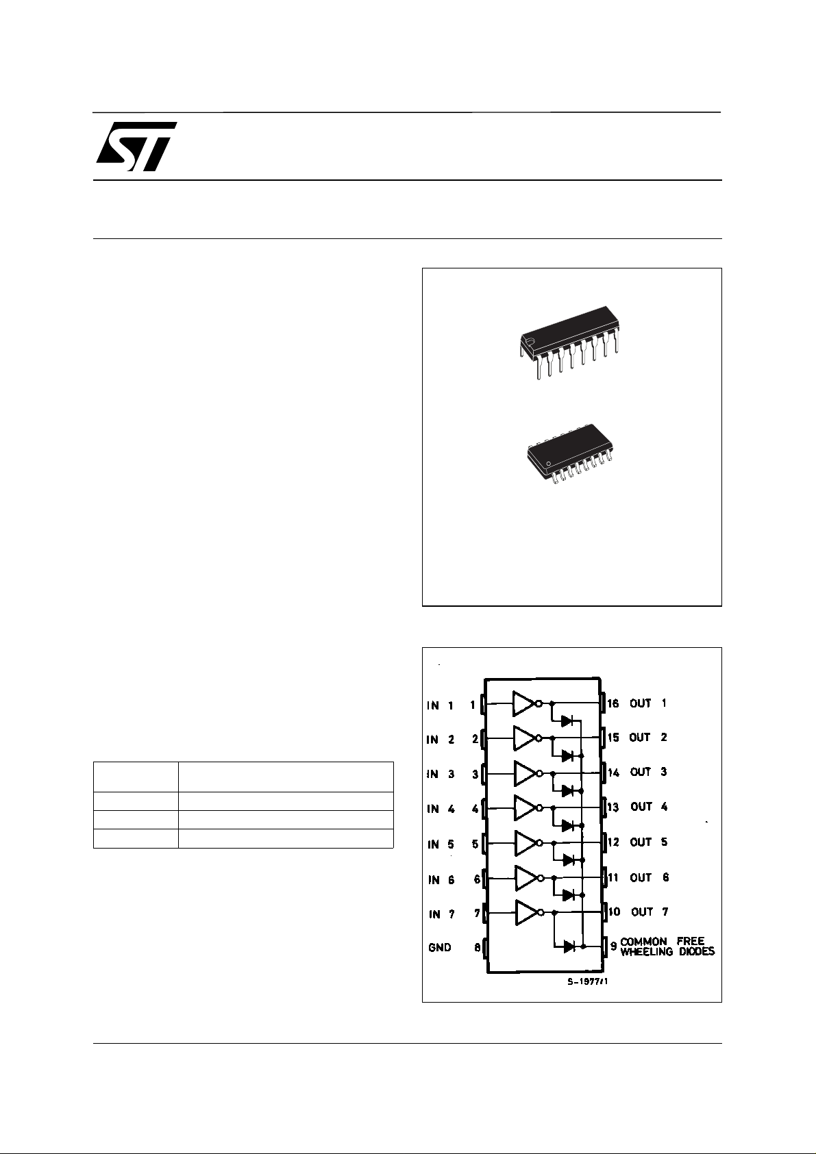
SEVEN DARLINGTONS PER PACKAGE
.
EXTENDED TEMPERATURE RANGE
.
(–40 to 105°C)
OUTPUT CURRENT 500 mA PER DRIVER
.
(600 mA PEAK)
OUTPUT V OLTAGE 50 V
.
INTEGRAL SUPPRESS ION DIODES FOR IN-
.
DUCTIVE LOADS
OUTPUTS CAN BE PARALLELED FOR
.
HIGHER CURRENT
TTL/CMOS/PMOS/DTL COMPA TIBLE INPU TS
.
INPUTS PINNED OPPOSITE OUTPUTS TO
.
SIMPLIFY LAYOUT
ULQ2002A - ULQ2004A
SEVEN DARLINGTON ARRAYS
DIP16
SO16
ORDERING NUMBERS:
DESCRIPTION
The ULQ2001A, ULQ2002A, ULQ2003 and
ULQ2004A are high voltage , high current darlin gton
arrays each containing seven open collector darlington pai rs with comm on emitters. E ach chann el is
rated at 500 m A and can w ithstand peak cu rrents of
600 mA. Su ppression diod es are inclu ded for inductive load drivi ng and the inp uts are pinn ed oppos ite
the outputs t o si mp lify board layout.
The four versi ons interface to all com mon logic families :
ULQ2001A General Purpose, DTL, TTL, PMOS,
CMOS
ULQ2002A 14-25V PMOS
ULQ2003A 5V TTL, CMOS
ULQ2004A 6-15V CMOS, PMOS
These ver satile de vices are usefu l for dri ving a wide
range of loads including solenoids, relays DC motors, LED displays filament lamps, thermal printheads and high power buffers .
The ULQ2001A/2002A/2 003A and 2004A are s upplied in 16 pin plastic DIP packages with a copper
leadframe to reduce thermal resistance. They are
available also in small outline package (SO-16) as
ULQ2001D1/2002D1/2003D1/2004D1.
ULQ2001 A/2 A/3 A/4 A (DI P16 )
ULQ2001 D1/2 D1/3D1 /4 D1 (SO 16)
PIN CONNECTION
February 2002
1/7
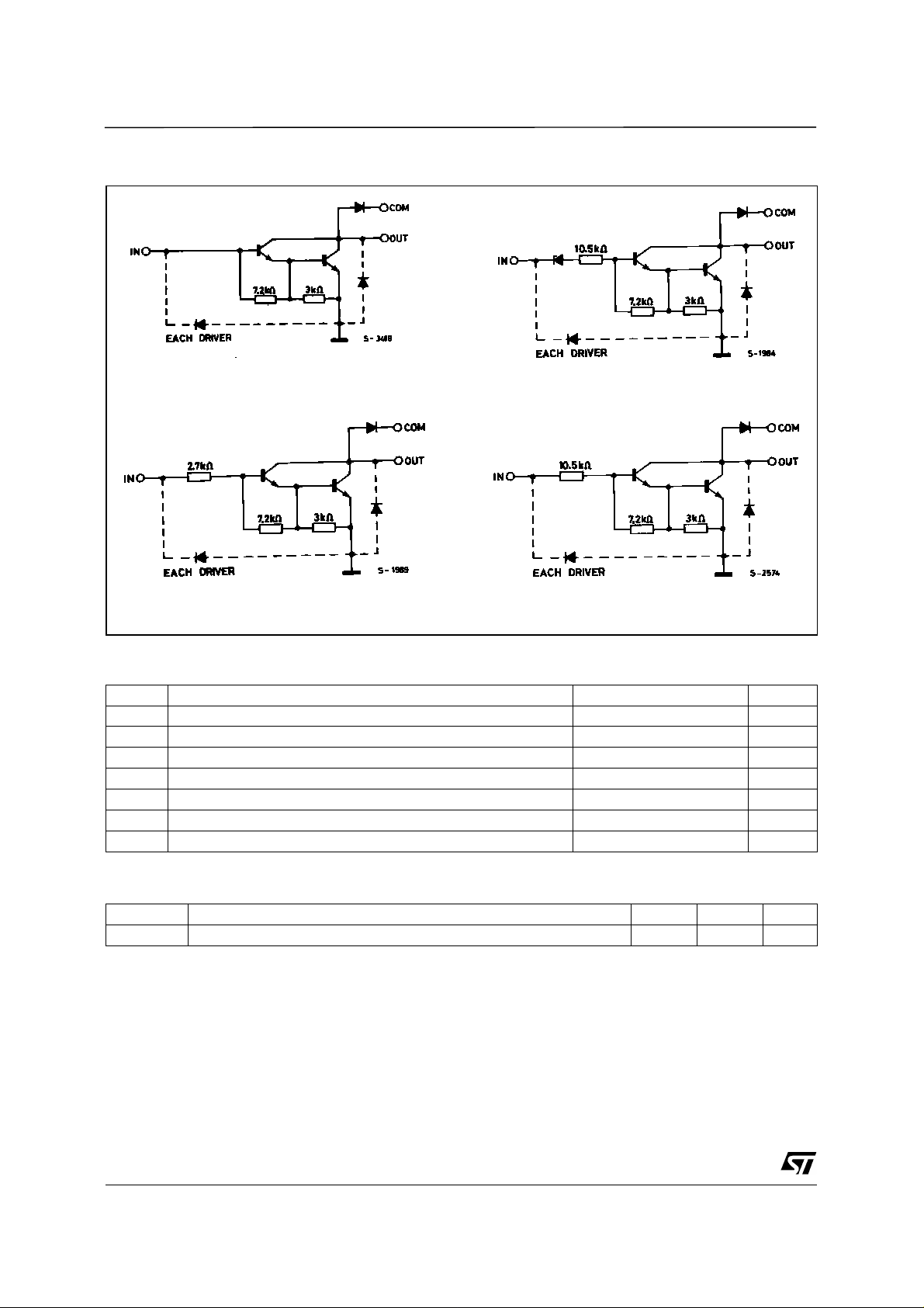
ULQ2001A - ULQ2002A - ULQ2003A - ULQ2004A
SCHEMATIC DIAGRAM
Series ULQ -20 01 A
(each driver)
Series ULQ -20 03 A
(each driver)
Series ULQ -20 02 A
(each driver)
Series ULQ -20 04 A
(each driver)
ABSOLUTE MAXIMUM RATIN GS
Symbol Parameter Value Unit
V
Output Voltage 50 V
o
V
Tamb
T
Input Voltage (for ULQ2002A/D1 - 2003A/D1 - 2004A/D1) 30 V
in
Continuous Colletor Current 500 mA
I
c
Continuous Base Current 25 mA
I
b
Operating Ambient Temperature Range –40 to 105 °C
Storage Temperature Range –55 to 150 °C
stg
Junction Temperature 150 °C
T
j
THERMAL DATA
Symbol Parameter DIP16 SO16 Unit
2/7
R
th j-amb
Thermal Resistance Junction-ambient Max. 70 120 °C/W
ULQ2001A - ULQ2002A - ULQ2003A - ULQ2004A
= –40 to 105oC for DIP16 unless otherwise specified)
ELECTRICAL CHARACTERISTICS
Symbol Parameter Test Conditions Min. Typ. Max. Unit Fig.
I
CEX
V
CE(sat )
I
i(on)
I
i(off)
V
h
t
PLH
t
PHL
(*) Guaranteed b y de sign
Output Leakage Current VCE = 50V
Collector-emitter
Saturation Voltage
Input Current for ULQ2002A Vi = 17V
Input Current TJ = 105°C, IC = 500µA5065µA4
Input Voltage for ULQ2002A VCE = 2V, IC = 300mA
i(on)
DC Forward Current Gain for ULQ2001A VCE = 2V, IC = 350mA 1000 – 2
FE
Input Capacitance 15 25 (*) pF –
C
i
Turn-on Delay Time 0.5 Vi to 0.5 V
Turn-off Delay Time 0.5 Vi to 0.5 V
Clamp Diode Leakage
I
R
Current
Clamp Diode Forward
V
F
Voltage
(T
J
(T
= 25 to 105oC for SO16 unless otherwise specified)
J
50
µA
TJ = 105°C, VCE = 50V
= 105°C
T
J
for ULQ2002A VCE = 50V, Vi = 6V
for ULQ2004A VCE = 50V, Vi = 1V
IC = 100mA, IB = 250µA
= 200mA, IB = 350µA
I
C
IC = 350mA, IB = 500µA
for ULQ2003A Vi = 3.85V
for ULQ2004A V
= 5V
i
Vi = 12V
for ULQ2003A VCE = 2V, IC = 200mA
VCE = 2V, IC = 250mA
= 2V, IC = 300mA
V
for ULQ2004A VCE = 2V, IC = 125mA
CE
VCE = 2V, IC = 200mA
= 2V, IC = 275mA
V
CE
VCE = 2V, IC = 350m A
o
o
VR = 50V
TJ = 105°C, VR = 50V
100
µA
500
µA
500
µA
0.9
1.1
1.3
0.82
0.93
0.35
1
1.1
1.3
1.6
1.25
1.35
0.5
1.45
13
2.4
2.7
V
V
V
mA
mA
mA
mA
V
V
V
3
V
5
V
6
V
7
V
8
V
0.25 1 (*) µs–
0.25 1 (*) µs–
50
100µAµA66
IF = 350mA 1.7 2 V 7
1a
1a
1b
1b
2
2
2
3
3
3
3
5
5
5
5
5
5
5
5
3/7
 Loading...