

Datasheet ULN2076B, ULN2074B, ULN2070B, ULN2068B, ULN2066B Datasheet (SGS Thomson Microelectronics)
...Page 1
50V- 1.5A QUADDARLINGTONSWITCHES
.OUTPUT CURRENT TO 1.5 A EACH DAR-
LINGTON
.MINIMUMBREAKDOWN50V
.SUSTAININGVOLTAGEATLEAST35 V
.
INTEGRAL SUPPRESSION DIODES
(ULN2064B, ULN2066B, ULN2068B and
ULN2070B)
.ISOLATED DARLINGTON PINOUT
(ULN2074B,ULN2076B)
.VERSIONS COMPATIBLE WITH ALL POPU-
LARLOGICFAMILIES
DESCRIP TION
Designedto interfacelogicto a widevarietyof high
current,highvoltageloads,thesedeviceseachcontain four NPN darlington switches delivering up to
1.5 A witha specifiedminimumbreakdownof 50 V
and a sustaining voltage of 35 V measuredat 100
mA. The ULN2064B, ULN2066B, ULN2068B and
ULN2070Bcontainintegralsuppressiondiodesfor
inductive loads have common emitters. The
ULN2074B and ULN2076B feature isolated darlington pinouts and are intended for applications
suchasemitterfollowerconfigurations.Inputsof the
ULN2064B, ULN2068B and ULN2074B are compatible with popular 5 V logic families and the
ULN2066Band ULN2076B are compatiblewith 615 V CMOS and PMOS. Types ULN2068B and
ULN2070Bincludeapredriverstagetoreduceloadingon the control logic.
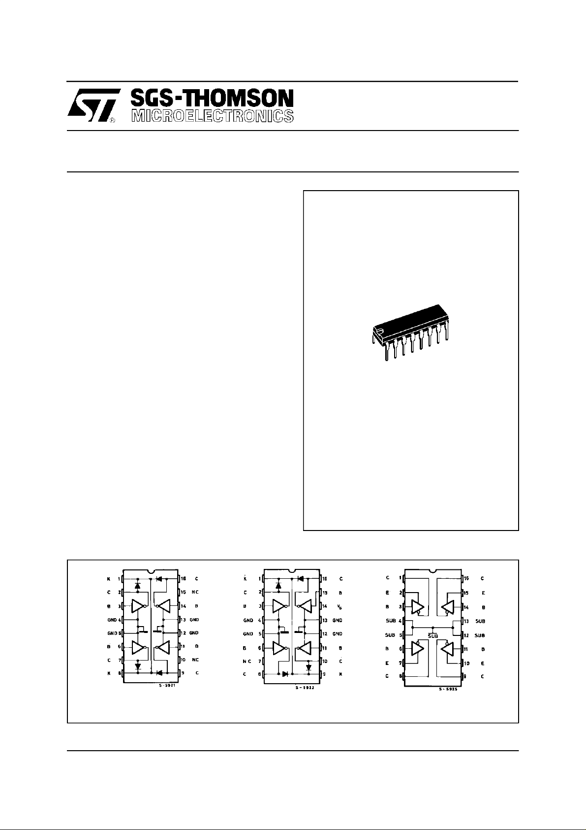
ULN2 064B - ULN2066B
ULN2068 B - ULN2070B
ULN2 074B - ULN2076B
PO W E RDIP
12 + 2 + 2
PIN CO NNECTI ONS AND O RDER CODES
ULN2064B
ULN2066B
April 1993
ULN2068B
ULN2070B
ULN2074B
ULN2076B
1/8
Page 2
ULN2064B-ULN2066B-ULN2068B-ULN2070B-ULN2074B-ULN2076B
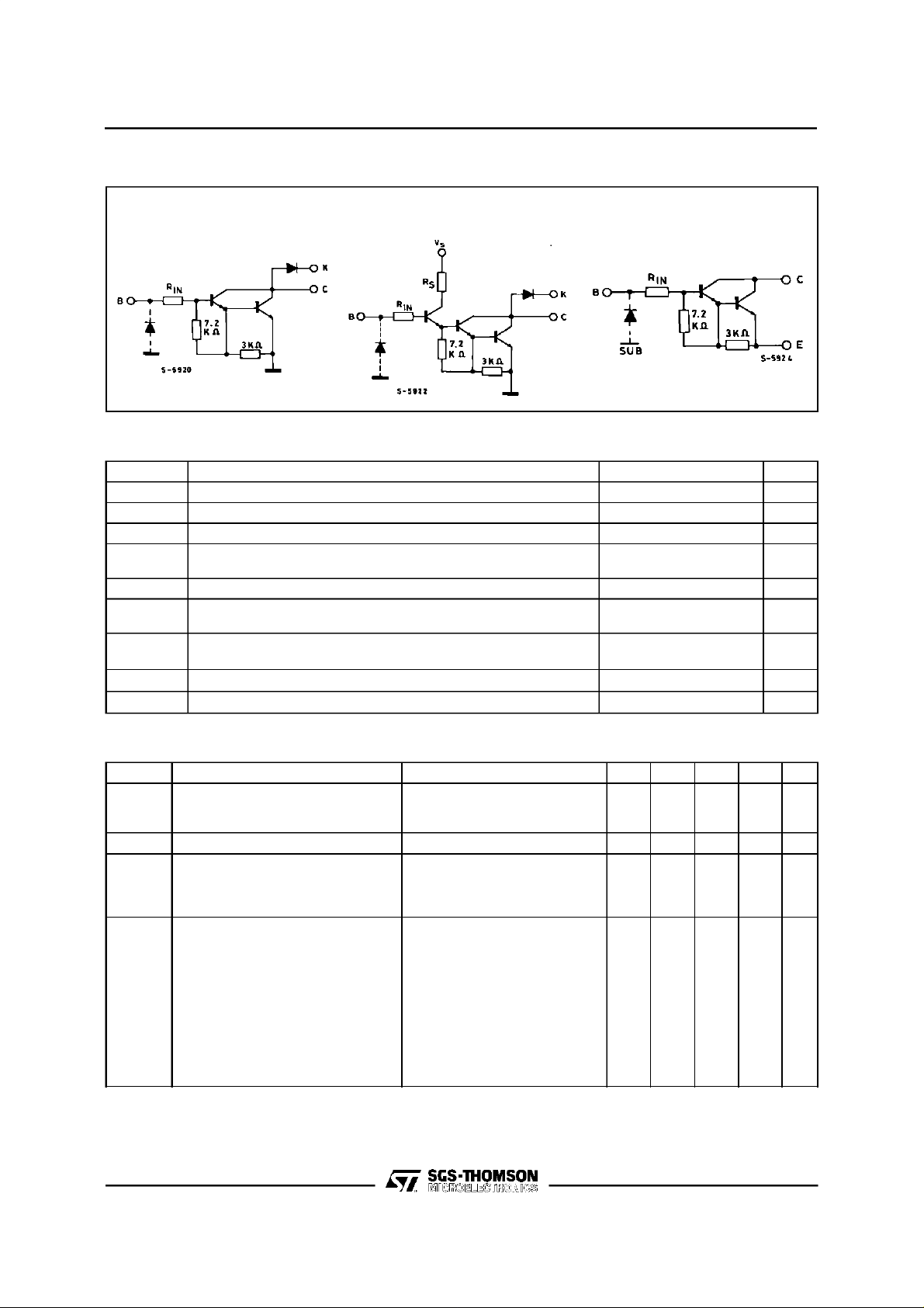
SCHEMATIC DI AGRAM
ULN2064B : RIN= 350
ULN2066B : R
IN
=3k
Ω
Ω
ULN2068B : R
ULN2070B : R
= 2.5kΩ,Rs= 900
IN
= 11.6kΩ,Rs= 3.4k
IN
Ω
Ω
ULN2074B : R
ULN2076B : R
IN
IN
= 350
=3k
Ω
ABSOLUTE MAXIMUM RATINGS
Symbol Parameter Value Unit
V
V
CE(sus)
P
T
T
CEX
I
O
V
I
V
tot
amb
stg
Output Voltage 50 V
Output Sustaining Voltage 35 V
Output Current 1.75 A
Input Voltage for ULN2066B – 2070B - 2074B - 2076B
i
Input Current 25 mA
I
Supply Voltage for ULN2068B
s
Power Dissipation at T
for ULN2064B – 2068B
for ULN2070B
=90°C
pins
at T
amb
=70°C
30
15
10
20
4.3
1
Operating Ambient Temperature Range – 20 to 85
Storage Temperature – 55 to 150
Ω
V
V
V
V
W
W
C
°
°C
(T
ELECTRICAL CHARACTERISTICS
=25oC unless otherwise specified )
amb
Symbol Parameter Test Conditions Min. Typ. Max. Unit Fig.
I
V
CE(sus)
V
CE(sat)
I
Output Leakage Current VCE= 50V
CEX
T
T
amb
amb
=25°C
=70°C
Collector-emitter Sustaining Voltage IC= 100mA, Vi= 0.4V 35 V 2
Collector-emitter Saturation Voltage
Input Current for ULN2064B and ULN2074B
i(on)
= 500mA IB= 625µA
I
C
I
= 750mA IB= 935µA
C
=1A IB= 1.25mA
I
C
= 1.25A IB= 2mA
I
C
= 2.4V
V
i
= 3.75V
V
i
for ULN2066B and ULN2076B
=5V
V
i
= 12V
V
i
for ULN2068B
= 2.75V
V
i
= 3.75V
V
i
for ULN2070B
=5V
V
i
= 12V
V
i
1.4
3.3
0.6
1.7
100
500
1.1
1.2
1.3
1.4
4.3
9.6
1.8
5.2
0.55
1.0
0.4
1.25
µA
µA
V
V
V
V
mA
mA
mA
mA
mA
mA
mA
mA
2/8
1
3
3
3
3
4
4
4
4
4
4
4
4
Page 3
ULN2064B-ULN2066B-ULN2068B-ULN2070B-ULN2074B-ULN2076B
ELECTRICAL CHARACTERISTICS (T
=25oC unless otherwise specified ) (continued)
amb
Symbol Parameter Test Conditions Min. Typ. Max. Unit Fig.
V
t
t
Notes :
Input Voltage VCE= 2V, IC=1A
i(on)
Supply Current for ULN2068B
I
s
Turn-on Delay Time 0.5 Vito 0.5 V
PLH
Turn-off Delay Time 0.5 Vito 0.5 V
PHL
Clamp Diode Leakage Current for ULN2064B-ULN2066B
I
R
Clamp Diode Forward Voltage for ULN2064B-ULN2066B
V
F
1. Input voltage is with reference to the substrate (no connection to any other pins) for the ULN2074B and ULN2076B
reference is ground for all other types.
2. Input current may be limited by maximum allowable input voltage.
ULN2064B, ULN2074B
ULN2066B, ULN2076B
= 2V, IC= 1.5A
V
CE
ULN2064B, ULN2074B
ULN2066B, ULN2076B
ULN2068B
ULN2070B
= 500mA, Vi= 2.75V
I
C
for ULN2070B
= 500mA, Vi=5V
I
C
o
o
and ULN2068B-ULN2070B
=50V
V
R
T
=25°C
amb
T
=70°C
amb
and ULN2068B-ULN2070B
=1A
I
F
= 1.5 A
I
F
2
6.5
2.5
10
2.75
5
6
4.5mAmA88
1 µ
1.5
50
100
1.752V
V
V
V
V
V
V
µ
µA
µA
V
s
s
5
5
5
5
5
5
6
7
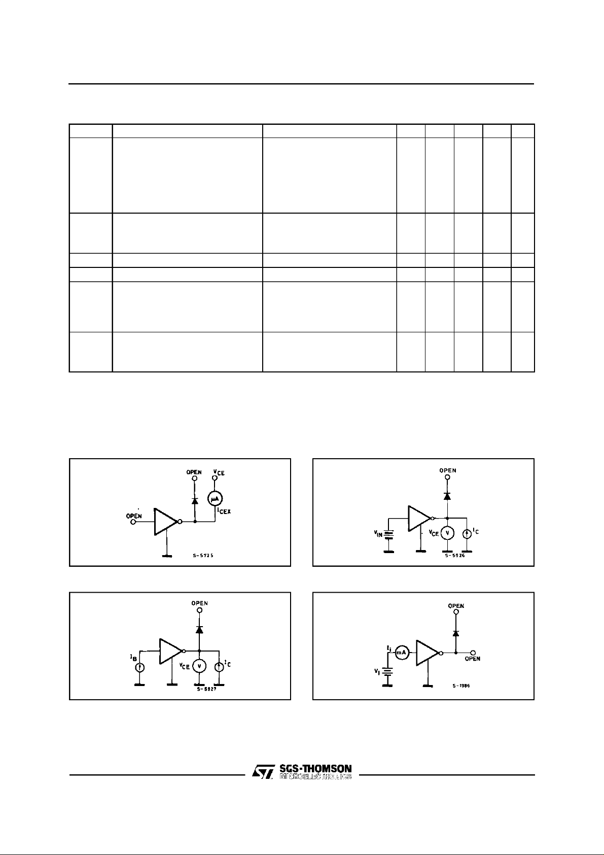
TEST CIRCUI TS
Figure1. Figure2.
Figure3. Figure4.
3/8
Page 4

ULN2064B-ULN2066B-ULN2068B-ULN2070B-ULN2074B-ULN2076B
Figure5. Figure6.
Figure7. Figure8.
Figure9 :
InputCurrent as a Functionof
InputVoltage.
Figure11 : CollectorCurrent as a Functionof
InputCurrent.
Figure10 :
InputCurrent as a Functionof
InputVoltage.
4/8
Page 5

ULN2064B-ULN2066B-ULN2068B-ULN2070B-ULN2074B-ULN2076B
MOUNTING INSTRUCTI O NS
TheR
pinsto a suitable copper area of the printedcircuit
board(Fig. 12) or to an externalheatsink(Fig. 13).
Thediagramof Figure 14 showsthemaximumdissipablepower P
theside”α” oftwo equalsquarecopperareashavinga thicknessof 35 µ (1.4mils).
canbe reducedby soldering the GND
th j-amb
andthe R
tot
th j-amb
asa functionof
Duringsolderingthepins temperaturemustnotexceed 260 °C and the soldering time must not be
longerthan 12seconds.
Theexternalheatsinkor printedcircuitcopperarea
mustbe connectedto electricalground.
Figure12 : Exampleof P.C.BoardArea whichis
Usedas Heatsink.
Figure14 :
MaximumDissipable Power and Junctionto AmbientThermalResistance
vs.Side”α”.
Figure13 : ExternalHeatsinkMounting Example.
Figure15 :
MaximumAllowablePowerDissipa-
tionvs. AmbientTemperature.
5/8
Page 6

ULN2064B-ULN2066B-ULN2068B-ULN2070B-ULN2074B-ULN2076B
TYPICAL APPLI CATIONS
Figure16 :
Common-anodeLEDDrivers.
Figure17 :
Common-cathodeLEDDrivers.
6/8
Page 7

ULN2064B-ULN2066B-ULN2068B-ULN2070B-ULN2074B-ULN2076B
POWERDIP 16 PACKAGE MECHANICAL DATA
DIM.
MIN. TYP. MAX. MIN. TYP. MAX.
a1 0.51 0.020
B 0.85 1.40 0.033 0.055
b 0.50 0.020
b1 0.38 0.50 0.015 0.020
D 20.0 0.787
E 8.80 0.346
e 2.54 0.100
e3 17.78 0.700
F 7.10 0.280
I 5.10 0.201
L 3.30 0.130
Z 1.27 0.050
mm inch
7/8
Page 8

ULN2064B-ULN2066B-ULN2068B-ULN2070B-ULN2074B-ULN2076B
Information furnished is believed to be accurate and reliable. However, SGS-THOMSON Microelectronics assumes no responsibility for
the consequences of use of such information nor for any infringement of patents or other rights of third parties which may result from its
use. No license is granted by implication or otherwise under any patent or patent rights of SGS-THOMSON Microelectronics. Specification
mentioned in this publication are subject to change without notice. This publication supersedes and replaces all information previously
supplied. SGS-THOMSON Microelectronics products are not authorized for use as critical components in life support devices or systems
without express written approval of SGS-THOMSON Microelectronics.
Australia - Brazil - Canada - China - France - Germany - Hong Kong - Italy - Japan - Korea - Malaysia - Malta - Morocco -
The Netherlands - Singapore - Spain - Sweden - Switzerland - Taiwan - Thailand - United Kingdom - U.S.A.
1996 SGS-THOMSON Microelectronics – Printed in Italy – All Rights Reserved
SGS-THOMSON Microelectronics GROUP OF COMPANIES
8/8
 Loading...