

STMicroelectronics ULN2064B, ULN2066B, ULN2074B, ULN2076B, ULN2068B Technical data
®
50V - 1.5A QUA D DARLINGT ON SWIT CHES
.
OUTPUT CURRENT TO 1.5 A EACH DARLINGTON
.
MINIMUM BREAKDOWN 50 V
.
SUSTAINING VOLTAGE AT LEAST 35 V
.
INTEGRAL SUPPRESSION DIODES
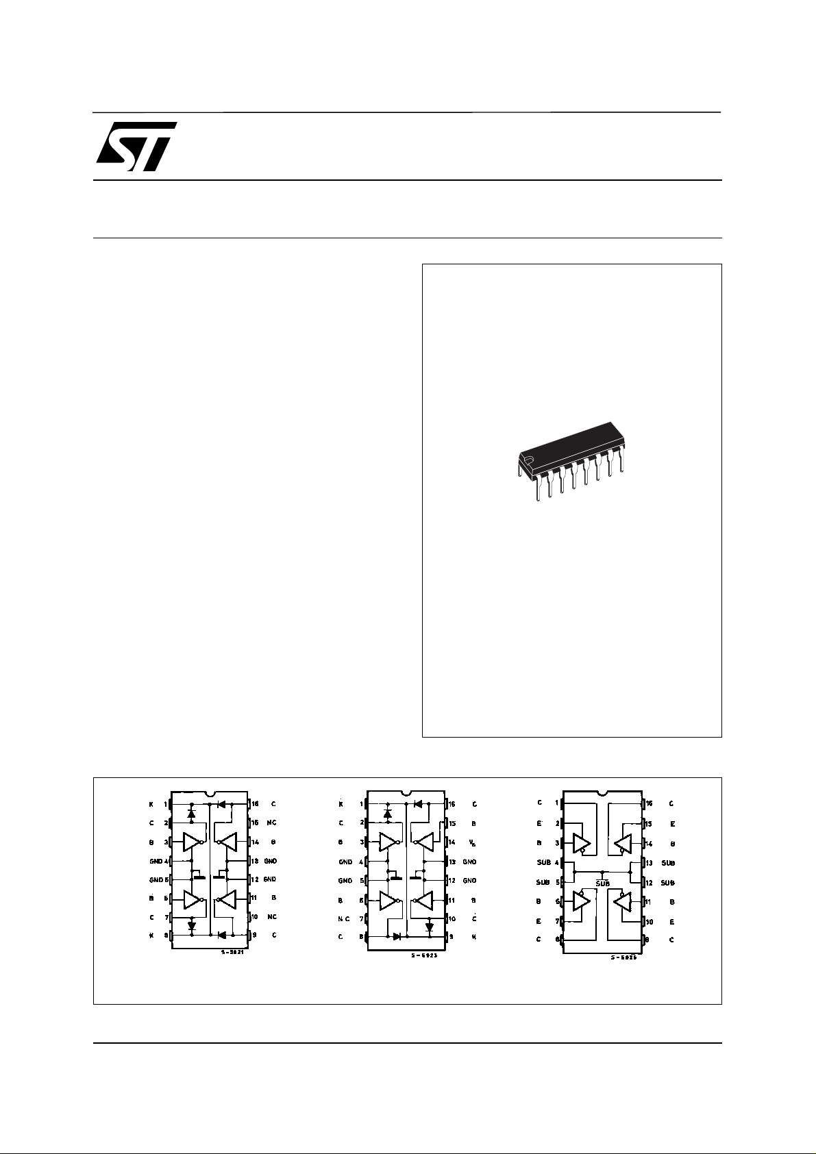
(ULN2064B, ULN2066B, ULN2068B and
ULN2070B)
.
ISOLATED DARLINGTON PINOUT
(ULN2074B , UL N2076B)
.
VERSIONS COMPATIBLE WITH ALL POPULAR LOGIC FAMILIES
DESCRIPTION
Designed to interface l ogic to a wi de v ari et y of high
current, high v oltage loads, these devic es each contain four NPN darlington switches delivering up to
1.5 A with a s pec ified minimum breakdown of 50 V
and a sustaining voltage of 35 V measured at 100
mA. The ULN2064B, ULN2066B, ULN2068B and
ULN2070B contain integral suppression diodes for
inductive loads have common emitters. The
ULN2074B and ULN2076B feature isolated darlington pinouts and are intended for applications
such as emitter follow er configur ations. Inpu ts of the
ULN2064B, ULN2068B and ULN2074B are compatible with popular 5 V logic families and the
ULN2066B and ULN2076B are compatible with 615 V CMOS and PMOS. Types ULN2068B and
ULN207 0B include a predriver s tage to reduce loading on the c ontr ol logic.
ULN2064B - ULN2066B
ULN2068B - ULN2070B
ULN2074B - ULN2076B
POWERDIP
12 + 2 + 2
PIN CONNECTIONS AND ORDER CODES
ULN2064B
ULN2066B
Septembe r 200 3
ULN2068B
ULN2070B
ULN2074B
ULN2076B
1/8
ULN2064B-ULN2066B-ULN2068B-ULN2070B-ULN2074B-ULN2076B
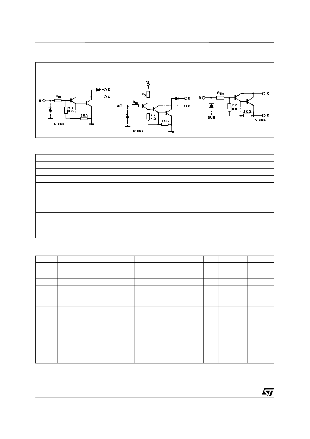
SCHEMATIC DIAGRAM
ULN2064B : RIN = 350
ULN2066B : R
IN
= 3k
Ω
Ω
ULN2068B : RIN = 2.5kΩ, Rs = 900
ULN2070B : R
= 11.6kΩ, Rs = 3.4k
IN
Ω
Ω
ULN2074B : RIN = 350
ULN2076B : R
IN
= 3k
Ω
ABSOLUTE MAXIMUM RATIN GS
Symbol Parameter Value Unit
V
V
CE(sus )
P
T
T
CEX
I
O
V
I
V
tot
amb
stg
Output Voltage 50 V
Output Sustaining Voltage 35 V
Output Current 1.75 A
Input Voltage for ULN2066B – 2070B - 2074B - 2076B
i
Input Current 25 mA
I
Supply Voltage for ULN2068B
s
Power Dissipation at T
for ULN2064B – 2068B
for ULN2070B
= 90 °C
pins
at T
= 70 °C
amb
30
15
10
20
4.3
1
Operating Ambient Temperature Range – 20 to 85
Storage Temperature – 55 to 150
Ω
V
V
V
V
W
W
C
°
C
°
= 25oC unless otherwise specified )
ELECTRICAL CHARACTERISTICS
(T
amb
Symbol Parameter Test Conditions Min. Typ. Max. Unit Fig.
I
V
CE(sus )
V
CE(sat)
I
CEX
i(on)
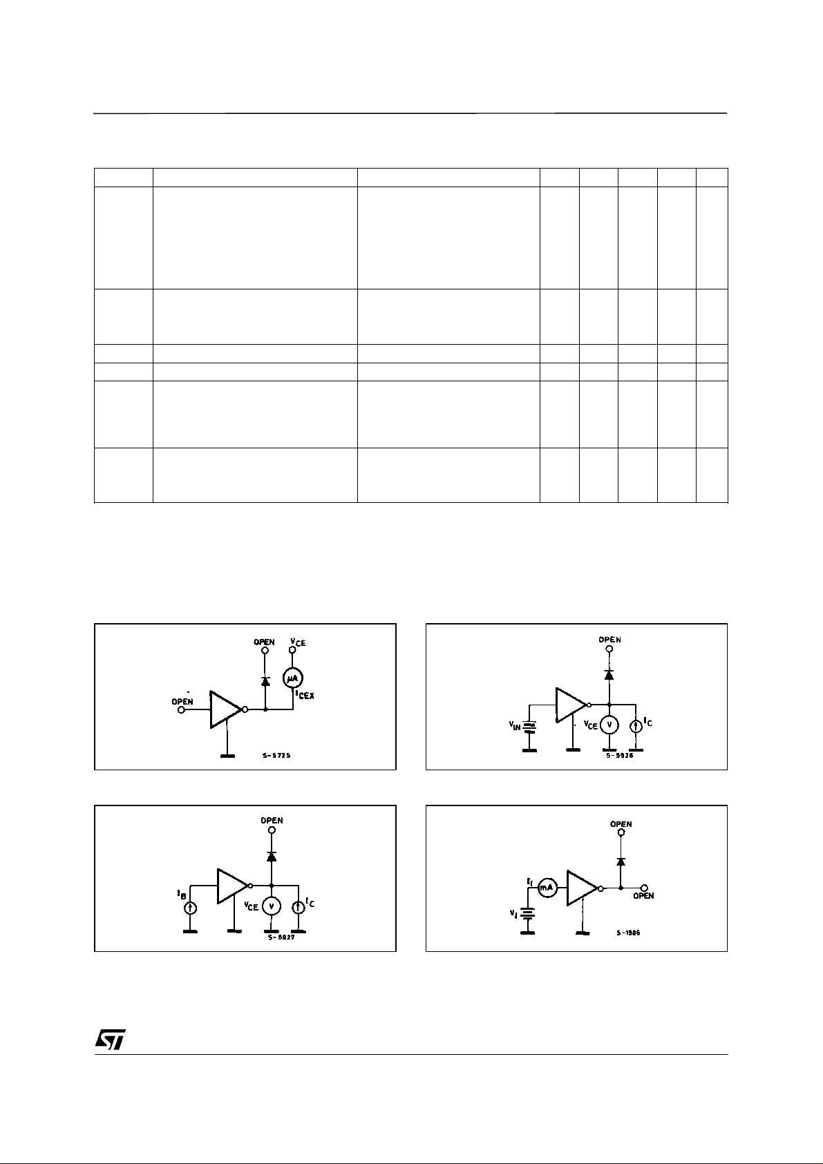
Output Leakage Current VCE = 50V
T
T
amb
amb
= 25°C
= 70°C
100
500
A
µ
A
µ
Collector-emitter Sustaining Voltage IC = 100mA, Vi = 0.4V 35 V 2
Collector-emitter Saturation Voltage IC = 500mA IB = 625µA
IC = 750mA IB = 935µA
IC = 1A IB = 1.25mA
IC = 1.25A IB = 2mA
1.1
1.2
1.3
1.4
V
V
V
V
Input Current for ULN2064B and ULN2074B
= 2.4V
V
i
Vi = 3.75V
1.4
3.3
4.3
9.6
mA
mA
for ULN2066B and ULN2076B
= 5V
V
i
Vi = 12V
0.6
1.7
1.8
5.2
mA
mA
for ULN2068B
= 2.75V
V
i
Vi = 3.75V
0.55
1.0
mA
mA
for ULN2070B
Vi = 5V
= 12V
V
i
0.4
1.25
mA
mA
2/8
1
3
3
3
3
4
4
4
4
4
4
4
4
ULN2064B-ULN2066B-ULN2068B-ULN2070B-ULN2074B-ULN2076B
= 25oC unless otherwise specified ) ( continued)
ELECTRICAL CHARACTERISTICS
Symbol Parameter Test Conditions Min. Typ. Max. Unit Fig.
V
t
t
Notes :
Input Voltage VCE = 2V, IC = 1A
i(on)
Supply Current for ULN2068B
I
s
Turn-on Delay Time 0.5 Vi to 0.5 V
PLH
Turn-off Delay Time 0.5 Vi to 0.5 V
PHL
Clamp Diode Leakage Current for ULN2064B-ULN2066B
I
R
V
Clamp Diode Forward Voltage for ULN2064B-ULN2066B
F
1. Input voltage is with reference to the substrate (no connection to any other pins) for the ULN2074B and ULN2076B
reference is ground for all other types.
2. Input current may be limited by maximum allowable input voltage.
(T
amb
ULN2064B, ULN2074B
ULN2066B, ULN2076B
= 2V, IC = 1.5A
V
CE
ULN2064B, ULN2074B
ULN2066B, ULN2076B
ULN2068B
ULN2070B
= 500mA, Vi = 2.75V
I
C
for ULN2070B
IC = 500mA, Vi = 5V
and ULN2068B-ULN2070B
= 50 V
V
R
T
= 25°C
amb
T
= 70°C
amb
and ULN2068B-ULN2070B
= 1 A
I
F
IF = 1.5 A
2
6.5
2.5
10
2.75
V
V
V
V
V
5
V
6
4.5mAmA88
o
o
1
1.5
50
100
s
µ
s
µ
A
µ
A
µ
1.752V
V
5
5
5
5
5
5
6
7
TEST CIRCUITS
Figure 1. Figure 2.
Figure 3. Figure 4.
3/8
 Loading...