

Page 1

Features
TO-220
• Output current up to 2 A
• Output voltages of 5; 7.5; 9; 10; 12; 15; 18; 24 V
• Thermal protection
• Short circuit protection
• Output transition SOA protection
L78S
2 A positive voltage regulator IC
Datasheet - production data
Description
The L78S series of three-terminal positive
regulators is available in TO-220 package and
several fixed output voltages, making it useful in a
wide range of applications. These regulators can
provide local on-card regulation, eliminating the
distribution problems assoc ia ted with sing le point
regulation. Each type embeds internal current
limiting, thermal shut-down and safe area
protection, making it essentially indestructible. If
adequate heat sinking is provided, they can
deliver over 2 A output current. Although
designed primarily as fixed voltage regulators,
these devices can be used with external
components to obtain adjustable voltages and
currents.
Table 1. Device summary
TO-220 packages
Part numbers
Dual gauge Single gauge
L78S05C L78S05CV-DG L78S05CV 5 V
L78S75C L78S75CV-DG L78S75CV 7.5 V
L78S09C L78S09CV-DG L78S09CV 9 V
L78S10C L78S10CV-DG L78S10CV 10 V
L78S12C L78S12CV-DG L78S12CV 12 V
L78S15C L78S15CV-DG L78S15CV 15 V
L78S18C L78S18CV 18 V
L78S24C L78S24CV 24 V
March 2014 DocID2148 Rev 8 1/35
This is information on a product in full production.
Output voltage
www.st.com
Page 2

Contents L78S
Contents
1 Diagram . . . . . . . . . . . . . . . . . . . . . . . . . . . . . . . . . . . . . . . . . . . . . . . . . . . 5
2 Pin configuration . . . . . . . . . . . . . . . . . . . . . . . . . . . . . . . . . . . . . . . . . . . 6
3 Maximum ratings . . . . . . . . . . . . . . . . . . . . . . . . . . . . . . . . . . . . . . . . . . . . 7
4 Test circuits . . . . . . . . . . . . . . . . . . . . . . . . . . . . . . . . . . . . . . . . . . . . . . . . 8
5 Electrical characteristics . . . . . . . . . . . . . . . . . . . . . . . . . . . . . . . . . . . . . 9
6 Typical performance . . . . . . . . . . . . . . . . . . . . . . . . . . . . . . . . . . . . . . . . 17
7 Package mechanical data . . . . . . . . . . . . . . . . . . . . . . . . . . . . . . . . . . . . 28
8 Packaging mechanical data . . . . . . . . . . . . . . . . . . . . . . . . . . . . . . . . . . 33
9 Revision history . . . . . . . . . . . . . . . . . . . . . . . . . . . . . . . . . . . . . . . . . . . 34
2/35 DocID2148 Rev 8
Page 3

L78S List of tables
List of tables
Table 1. Device summary . . . . . . . . . . . . . . . . . . . . . . . . . . . . . . . . . . . . . . . . . . . . . . . . . . . . . . . . . . 1
Table 2. Absolute maximum ratings . . . . . . . . . . . . . . . . . . . . . . . . . . . . . . . . . . . . . . . . . . . . . . . . . . 7
Table 3. Thermal data. . . . . . . . . . . . . . . . . . . . . . . . . . . . . . . . . . . . . . . . . . . . . . . . . . . . . . . . . . . . . 7
Table 4. Electrical characteristics of L78S05C . . . . . . . . . . . . . . . . . . . . . . . . . . . . . . . . . . . . . . . . . . 9
Table 5. Electrical characteristics of L78S75C . . . . . . . . . . . . . . . . . . . . . . . . . . . . . . . . . . . . . . . . . 10
Table 6. Electrical characteristics of L78S09C . . . . . . . . . . . . . . . . . . . . . . . . . . . . . . . . . . . . . . . . . 11
Table 7. Electrical characteristics of L78S10C . . . . . . . . . . . . . . . . . . . . . . . . . . . . . . . . . . . . . . . . . 12
Table 8. Electrical characteristics of L78S12C . . . . . . . . . . . . . . . . . . . . . . . . . . . . . . . . . . . . . . . . . 13
Table 9. Electrical characteristics of L78S15C . . . . . . . . . . . . . . . . . . . . . . . . . . . . . . . . . . . . . . . . . 14
Table 10. Electrical characteristics of L78S18C . . . . . . . . . . . . . . . . . . . . . . . . . . . . . . . . . . . . . . . . . 15
Table 11. Electrical characteristics of L78S24C . . . . . . . . . . . . . . . . . . . . . . . . . . . . . . . . . . . . . . . . . 16
Table 12. TO-220 (dual gauge) mechanical data . . . . . . . . . . . . . . . . . . . . . . . . . . . . . . . . . . . . . . . . 30
Table 13. TO-220 SG (single gauge) mechanical data . . . . . . . . . . . . . . . . . . . . . . . . . . . . . . . . . . . 32
Table 14. Document revision history . . . . . . . . . . . . . . . . . . . . . . . . . . . . . . . . . . . . . . . . . . . . . . . . . 34
DocID2148 Rev 8 3/35
35
Page 4

List of figures L78S
List of figures
Figure 1. Block diagram. . . . . . . . . . . . . . . . . . . . . . . . . . . . . . . . . . . . . . . . . . . . . . . . . . . . . . . . . . . . 5
Figure 2. Pin connections (top view) . . . . . . . . . . . . . . . . . . . . . . . . . . . . . . . . . . . . . . . . . . . . . . . . . . 6
Figure 3. Schematic diagram . . . . . . . . . . . . . . . . . . . . . . . . . . . . . . . . . . . . . . . . . . . . . . . . . . . . . . . . 6
Figure 4. Application circuits . . . . . . . . . . . . . . . . . . . . . . . . . . . . . . . . . . . . . . . . . . . . . . . . . . . . . . . . 7
Figure 5. DC parameter . . . . . . . . . . . . . . . . . . . . . . . . . . . . . . . . . . . . . . . . . . . . . . . . . . . . . . . . . . . . 8
Figure 6. Load regulation. . . . . . . . . . . . . . . . . . . . . . . . . . . . . . . . . . . . . . . . . . . . . . . . . . . . . . . . . . . 8
Figure 7. Ripple rejection. . . . . . . . . . . . . . . . . . . . . . . . . . . . . . . . . . . . . . . . . . . . . . . . . . . . . . . . . . . 8
Figure 8. Dropout voltage vs. junction temperature. . . . . . . . . . . . . . . . . . . . . . . . . . . . . . . . . . . . . . 17
Figure 9. Peak output current vs. input/output differential voltage. . . . . . . . . . . . . . . . . . . . . . . . . . . 17
Figure 10. Output impedance vs. frequency . . . . . . . . . . . . . . . . . . . . . . . . . . . . . . . . . . . . . . . . . . . . 17
Figure 11. Output voltage vs. junction temperature . . . . . . . . . . . . . . . . . . . . . . . . . . . . . . . . . . . . . . . 17
Figure 12. Supply voltage rejection vs. frequency . . . . . . . . . . . . . . . . . . . . . . . . . . . . . . . . . . . . . . . . 18
Figure 13. Quiescent current vs. junction temperature . . . . . . . . . . . . . . . . . . . . . . . . . . . . . . . . . . . . 18
Figure 14. Load transient response . . . . . . . . . . . . . . . . . . . . . . . . . . . . . . . . . . . . . . . . . . . . . . . . . . . 18
Figure 15. Line transient response . . . . . . . . . . . . . . . . . . . . . . . . . . . . . . . . . . . . . . . . . . . . . . . . . . . 18
Figure 16. Quiescent current vs. input voltage . . . . . . . . . . . . . . . . . . . . . . . . . . . . . . . . . . . . . . . . . . 18
Figure 17. Fixed output regulator. . . . . . . . . . . . . . . . . . . . . . . . . . . . . . . . . . . . . . . . . . . . . . . . . . . . . 19
Figure 18. Constant current regulator . . . . . . . . . . . . . . . . . . . . . . . . . . . . . . . . . . . . . . . . . . . . . . . . . 19
Figure 19. Circuit for increasing output voltage . . . . . . . . . . . . . . . . . . . . . . . . . . . . . . . . . . . . . . . . . . 19
Figure 20. Adjustable output regulator (7 to 30 V). . . . . . . . . . . . . . . . . . . . . . . . . . . . . . . . . . . . . . . . 20
Figure 21. 0.5 to 10 V regulator . . . . . . . . . . . . . . . . . . . . . . . . . . . . . . . . . . . . . . . . . . . . . . . . . . . . . . 20
Figure 22. High current voltage regulator . . . . . . . . . . . . . . . . . . . . . . . . . . . . . . . . . . . . . . . . . . . . . . 21
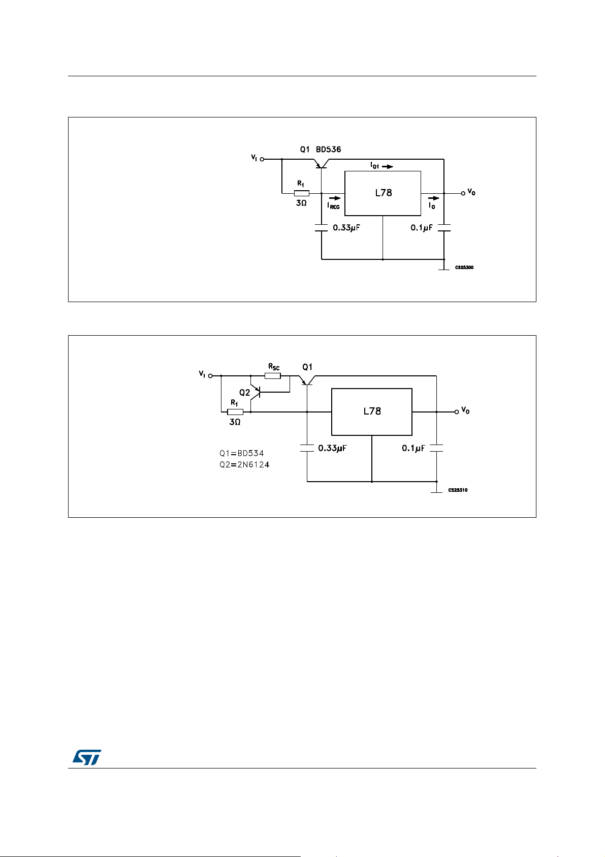
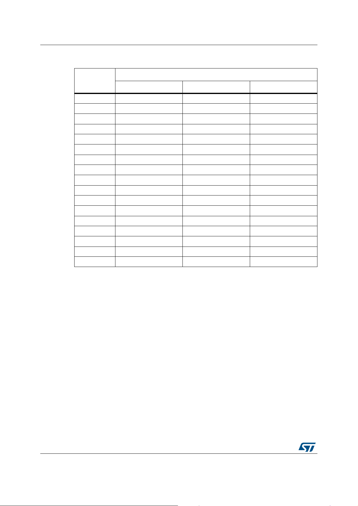
Figure 23. High output current with short circuit protection . . . . . . . . . . . . . . . . . . . . . . . . . . . . . . . . . 21
Figure 24. Tracking voltage regulator . . . . . . . . . . . . . . . . . . . . . . . . . . . . . . . . . . . . . . . . . . . . . . . . . 22
Figure 25. Positive and negative regulator . . . . . . . . . . . . . . . . . . . . . . . . . . . . . . . . . . . . . . . . . . . . . 22
Figure 26. Negative output voltage circuit . . . . . . . . . . . . . . . . . . . . . . . . . . . . . . . . . . . . . . . . . . . . . . 23
Figure 27. Switching regulator . . . . . . . . . . . . . . . . . . . . . . . . . . . . . . . . . . . . . . . . . . . . . . . . . . . . . . . 23
Figure 28. High input voltage circuit. . . . . . . . . . . . . . . . . . . . . . . . . . . . . . . . . . . . . . . . . . . . . . . . . . . 23
Figure 29. High input voltage circuit. . . . . . . . . . . . . . . . . . . . . . . . . . . . . . . . . . . . . . . . . . . . . . . . . . . 24
Figure 30. High output voltage regulator . . . . . . . . . . . . . . . . . . . . . . . . . . . . . . . . . . . . . . . . . . . . . . . 24
Figure 31. High input and output voltage. . . . . . . . . . . . . . . . . . . . . . . . . . . . . . . . . . . . . . . . . . . . . . . 24
Figure 32. Reducing power dissipation with dropping resistor. . . . . . . . . . . . . . . . . . . . . . . . . . . . . . . 25
Figure 33. Remote shutdown. . . . . . . . . . . . . . . . . . . . . . . . . . . . . . . . . . . . . . . . . . . . . . . . . . . . . . . . 25
Figure 34. Power AM modulator (unity voltage gain, I
Figure 35. Adjustable output voltage with temperature compensation . . . . . . . . . . . . . . . . . . . . . . . . 26
Figure 36. Light controllers (V
Figure 37. Protection against input short-circuit with high capacitance loads . . . . . . . . . . . . . . . . . . . 27
Figure 38. TO-220 (dual gauge) drawing. . . . . . . . . . . . . . . . . . . . . . . . . . . . . . . . . . . . . . . . . . . . . . . 29
Figure 39. TO-220 SG (single gauge) drawing . . . . . . . . . . . . . . . . . . . . . . . . . . . . . . . . . . . . . . . . . . 31
Figure 40. Tube for TO-220 (dual gauge) (mm.) . . . . . . . . . . . . . . . . . . . . . . . . . . . . . . . . . . . . . . . . . 33
Figure 41. Tube for TO-220 (single gauge) (mm.). . . . . . . . . . . . . . . . . . . . . . . . . . . . . . . . . . . . . . . . 33
= VXX + VBE). . . . . . . . . . . . . . . . . . . . . . . . . . . . . . . . . . . . . . . . . 27
Omin
£ 1 A) . . . . . . . . . . . . . . . . . . . . . . . . . . . . . . 26
O
4/35 DocID2148 Rev 8
Page 5

L78S Diagram
1 Diagram
Figure 1. Block diagram
DocID2148 Rev 8 5/35
35
Page 6

Pin configuration L78S
72
*5281'*5281'
2 Pin configuration
Figure 2. Pin connections (top view)
Figure 3. Schematic diagram
6/35 DocID2148 Rev 8
Page 7

L78S Maximum ratings
4
3 Maximum ratings
Table 2. Absolute maximum ratings
Symbol Parameter Value Unit
for V
= 5 to 18V 35
O
= 24V 40
for V
O
V
T
P
T
V
I
STG
OP
DC input voltage
I
Output current Internally limited
O
Power dissipation Internally limited
D
Storage temperature range -65 to 150 °C
Operating junction temperature range 0 to 150 °C
Note: Absolute maximum ratings are those values beyond which damage to the device may occur.
Functional operation under these condition is not implied.
Table 3. Thermal data
Symbol Parameter TO-220 Unit
R
thJC
R
thJA
Thermal resistance junc tion-case 5 °C/W
Thermal resistance junction-ambient 50 °C/W
Figure 4. Application circuits
DocID2148 Rev 8 7/35
35
Page 8

Test circuits L78S
4
4
4
4 Test circuits
Figure 5. DC parameter
Figure 6. Load regulation
Figure 7. Ripple rejection
8/35 DocID2148 Rev 8
Page 9

L78S Electrical characterist ics
5 Electrical characteristics
Refer to the test circuits, TJ = 25 °C, VI = 10 V, IO = 500 mA, unless otherwise specified.
Symbol Parameter Test conditions Min. Typ. Max. Unit
T able 4. Electrical characteristics of L78S05C
V
V
ΔV
ΔV
ΔI
Output voltage 4.8 5 5.2 V
O
Output voltage IO = 1 A, VI = 7 V 4.75 5 5.25 V
O
= 7 to 25 V 100
V
Line regulation
O
Load regulation
O
I
Quiescent curr ent 8 mA
Q
Quiescent current change
Q
I
VI = 8 to 25 V 50
I
= 20 mA to 1.5 A 100
O
= 2 A 80
I
O
I
= 20 mA to 1 A 0.5
O
= 7 to 25 V, IO = 20 mA 1.3
V
I
ΔVO/ΔT Output voltage drift IO = 5 mA, TJ = 0 °C to 70 °C -1.1 mV/°C
eN Output noise voltage B = 10 Hz to 100 kHz 40 µV
SVR Supply voltage rejection f = 120 Hz 54
V
Operating input voltage IO ≤ 1 A 8 V
I
R
I
I
1. Guaranteed by design.
Output resistance f = 1 kHz 17 mΩ
O
Short circuit current VI = 27 V 500 mA
sc
Short circuit peak current 3 A
scp
(1)
mV
mV
mA
dB
DocID2148 Rev 8 9/35
35
Page 10

Electrical characteristics L78S
Refer to the test circuits, TJ = 25 °C, VI = 12.5 V, IO = 500 mA, unless otherwise specified.
Symbol Parameter Test conditions Min. Typ. Max. Unit
T able 5. Electrical characteristics of L78S75C
V
V
ΔV
ΔV
ΔI
ΔV
Output voltage 7.15 7.5 7.9 V
O
Output voltage IO = 1 A, VI = 9.5 V 7.1 7.5 7.95 V
O
V
= 9.5 to 25 V 120
Line regulation
O
Load regulation
O
I
Quiescent curr ent 8 mA
Q
Quiescent current change
Q
/ΔT Output voltage drift IO = 5 mA, TJ = 0 °C to 70 °C -0.8 mV/°C
O
I
= 10.5 to 20 V 60
V
I
= 20 mA to 1.5 A 140
I
O
IO = 2 A 100
= 20 mA to 1 A 0.5
I
O
VI = 9.5 to 25 V, IO = 20 mA 1.3
eN Output noise voltage B = 10 Hz to 100 kHz 52 µV
SVR Supply voltage rejection f = 120 Hz 48
V
Operating input voltage IO ≤ 1 A 10. 5 V
I
R
I
I
1. Guaranteed by design.
Output resistance f = 1 kHz 16 mΩ
O
Short circuit current VI = 27 V 500 mA
sc
Short circuit peak current 3 A
scp
(1)
mV
mV
mA
dB
10/35 DocID2148 Rev 8
Page 11

L78S Electrical characterist ics
Refer to the test circuits, TJ = 25 °C, VI = 14 V, IO = 500 mA, unless otherwise specified.
Symbol Parameter Test conditions Min. Typ. Max. Unit
T able 6. Electrical characteristics of L78S09C
V
V
ΔV
ΔV
ΔI
ΔV
Output voltage 8.65 9 9.35 V
O
Output voltage IO = 1 A, VI = 11 V 8.6 9 9.4 V
O
V
= 11 to 25 V 130
Line regulation
O
Load regulation
O
I
Quiescent curr ent 8 mA
Q
Quiescent current change
Q
/ΔT Output voltage drift IO = 5 mA, TJ = 0 °C to 70 °C -1 mV/°C
O
I
= 11 to 20 V 65
V
I
= 20 mA to 1.5 A 170
I
O
IO = 2 A 100
= 20 mA to 1 A 0.5
I
O
VI = 11 to 25 V, IO = 20 mA 1.3
eN Output noise voltage B = 10 Hz to 100 kHz 60 µV
SVR Supply voltage rejection f = 120 Hz 47
V
Operating input voltage IO ≤ 1 A 12 V
I
R
I
I
1. Guaranteed by design.
Output resistance f = 1 kHz 17 mΩ
O
Short circuit current VI = 27 V 500 mA
sc
Short circuit peak current 3 A
scp
(1)
mV
mV
mA
dB
DocID2148 Rev 8 11/35
35
Page 12
Electrical characteristics L78S
Refer to the test circuits, TJ = 25 °C, VI = 15 V, IO = 500 mA, unless otherwise specified.
Symbol Parameter Test conditions Min. Typ. Max. Unit
T able 7. Electrical characteristics of L78S10C
V
V
ΔV
ΔV
ΔI
ΔV
Output voltage 9.5 10 10.5 V
O
Output voltage IO = 1 A, VI = 12.5 V 9.4 10 10.6 V
O
V
= 12.5 to 30 V 200
Line regulation
O
Load regulation
O
I
Quiescent curr ent 8 mA
Q
Quiescent current change
Q
/ΔT Output voltage drift IO = 5 mA, TJ = 0 °C to 70 °C -1 mV/°C
O
I
= 14 to 22 V 100
V
I
= 20 mA to 1.5 A 240
I
O
IO = 2 A 150
= 20 mA to 1 A 0.5
I
O
VI = 12.5 to 30 V, IO = 20 mA 1
eN Output noise voltage B = 10 Hz to 100 kHz 65 µV
SVR Supply voltage rejection f = 120 Hz 47
V
Operating input voltage IO ≤ 1 A 13 V
I
R
I
I
1. Guaranteed by design.
Output resistance f = 1 kHz 17 mΩ
O
Short circuit current VI = 27 V 500 mA
sc
Short circuit peak current 3 A
scp
(1)
mV
mV
mA
dB
12/35 DocID2148 Rev 8
Page 13
L78S Electrical characterist ics
Refer to the test circuits, TJ = 25 °C, VI = 19 V, IO = 500 mA, unless otherwise specified.
Symbol Parameter Test conditions Min. Typ. Max. Unit
T able 8. Electrical characteristics of L78S12C
V
V
ΔV
ΔV
ΔI
ΔV
Output voltage 11.5 12 12.5 V
O
Output voltage IO = 1 A, VI = 14.5 V 11.4 12 12.6 V
O
V
= 14.5 to 30 V 240
Line regulation
O
Load regulation
O
I
Quiescent curr ent 8 mA
Q
Quiescent current change
Q
/ΔT Output voltage drift IO = 5 mA, TJ = 0 °C to 70 °C -1 mV/°C
O
I
= 16 to 22 V 120
V
I
= 20 mA to 1.5 A 240
I
O
IO = 2 A 150
= 20 mA to 1 A 0.5
I
O
VI = 14.5 to 30 V, IO = 20 mA 1
eN Output noise voltage B =10 Hz to 100 kHz 75 µV
SVR Supply voltage rejection f = 120 Hz 47
V
Operating input voltage IO ≤ 1 A 15 V
I
R
I
I
1. Guaranteed by design.
Output resistance f = 1 kHz 18 mΩ
O
Short circuit current VI = 27 V 500 mA
sc
Short circuit peak current 3 A
scp
(1)
mV
mV
mA
dB
DocID2148 Rev 8 13/35
35
Page 14

Electrical characteristics L78S
Refer to the test circuits, TJ = 25 °C, VI = 23 V, IO = 500 mA, unless otherwise specified.
Symbol Parameter Test conditions Min. Typ. Max. Unit
T able 9. Electrical characteristics of L78S15C
V
V
ΔV
ΔV
ΔI
ΔV
Output voltage 14.4 15 15.6 V
O
Output voltage IO = 1 A, VI = 17.5 V 14.25 15 15.75 V
O
V
= 17.5 to 30 V 300
Line regulation
O
Load regulation
O
I
Quiescent curr ent 8 mA
Q
Quiescent current change
Q
/ΔT Output voltage drift IO = 5 mA, TJ = 0 °C to 70 °C -1 mV/°C
O
I
= 20 to 26 V 150
V
I
= 20 mA to 1.5 A 300
I
O
IO = 2 A 150
= 20 mA to 1 A 0.5
I
O
VI = 17.5 to 30 V, IO = 20 mA 1
eN Output noise voltage B =10 Hz to 100 kHz 90 µV
SVR Supply voltage rejection f = 120 Hz 46
V
Operating input voltage IO ≤ 1 A 18 V
I
R
I
I
1. Guaranteed by design.
Output resistance f = 1 kHz 19 mΩ
O
Short circuit current VI = 27 V 500 mA
sc
Short circuit peak current 3 A
scp
(1)
mV
mV
mA
dB
14/35 DocID2148 Rev 8
Page 15

L78S Electrical characterist ics
Refer to the test circuits, TJ = 25 °C, VI = 26 V, IO = 500 mA, unless otherwise specified.
Symbol Parameter Test conditions Min. Typ. Max. Unit
Table 10. Electrical characteristics of L78S18C
V
V
ΔV
ΔV
ΔI
ΔV
Output voltage 17.1 18 18.9 V
O
Output voltage IO = 1 A, VI = 20.5 V 17 18 19 V
O
V
= 20.5 to 30 V 360
Line regulation
O
Load regulation
O
I
Quiescent curr ent 8 mA
Q
Quiescent current change
Q
/ΔT Output voltage drift IO = 5 mA, TJ = 0 °C to 70 °C -1 mV/°C
O
I
= 22 to 28 V 180
V
I
= 20 mA to 1.5 A 360
I
O
IO = 2 A 200
= 20 mA to 1 A 0.5
I
O
VI = 20.5 to 30 V, IO = 20 mA 1
eN Output noise voltage B =10 Hz to 100 kHz 110 µV
SVR Supply voltage rejection f = 120 Hz 43
V
Operating input voltage IO ≤ 1 A 21 V
I
R
I
I
1. Guaranteed by design.
Output resistance f = 1 kHz 22 mΩ
O
Short circuit current VI = 27 V 500 mA
sc
Short circuit peak current 3 A
scp
(1)
mV
mV
mA
dB
DocID2148 Rev 8 15/35
35
Page 16

Electrical characteristics L78S
Refer to the test circuits, TJ = 25 °C, VI = 33 V, IO = 500 mA, unless otherwise specified.
Symbol Parameter Test conditions Min. Typ. Max. Unit
Table 11. Electrical characteristics of L78S24C
V
V
ΔV
ΔV
ΔI
ΔV
Output voltage 23 24 25 V
O
Output voltage IO = 1 A, VI = 27 V 22.82425.2 V
O
V
= 27 to 38 V 480
Line regulation
O
Load regulation
O
I
Quiescent curr ent 8 mA
Q
Quiescent current change
Q
/ΔT Output voltage drift IO = 5 mA, TJ = 0 °C to 70 °C -1.5 mV/°C
O
I
= 30 to 36 V 240
V
I
= 20 mA to 1.5 A 480
I
O
IO = 2 A 300
= 20 mA to 1 A 0.5
I
O
VI = 27 to 38 V, IO = 20 mA 1
eN Output noise voltage B = 10 Hz to 100 kHz 170 µV
SVR Supply voltage rejection f = 120 Hz 42
V
Operating input voltage IO ≤ 1 A 27 V
I
R
I
I
1. Guaranteed by design.
Output resistance f = 1 kHz 28 mΩ
O
Short circuit current VI = 27 V 500 mA
sc
Short circuit peak current 3 A
scp
(1)
mV
mV
mA
dB
16/35 DocID2148 Rev 8
Page 17
L78S Typical performance
6 Typical performance
Figure 8. Dropout voltage vs. junction
temperature
Figure 9. Peak output current vs. input/output
differential voltage
Figure 10. Output impedance vs. frequency Figure 11. Output voltage vs. junction
temperature
DocID2148 Rev 8 17/35
35
Page 18

Typical performance L78S
Figure 12. Supply voltage rejection vs.
Figure 14. Load transient response Figure 15. Line transient response
frequency
Figure 13. Quiescent current vs. junction
temperature
Figure 16. Quiescent current vs. input voltage
18/35 DocID2148 Rev 8
Page 19

L78S Typical performance
,2 9
;;;;5,G
4
,5,
G
92 9
;;;;
555,G5
Ż
4
Figure 17. Fixed output regulator
1. Although no output capacitor is need for stability, it does improve transient response.
2. Required if regulator is located an appreciable distance from power supply filter.
Figure 18. Constant current regulato r
Figure 19. Circuit for increasing output voltage
DocID2148 Rev 8 19/35
35
Page 20
Typical performance L78S
VO=VXXR4/R
1
Figure 20. Adjustable output regulator (7 to 30 V)
Figure 21. 0.5 to 10 V regulator
20/35 DocID2148 Rev 8
Page 21
L78S Typical performance
5
,2 ,
5(*
4,
5(*
B9BBBB
%(4
B
9
%(4
5 BBBBBBBBBBBBBB
,
5(4
,4E4
4
5
6&6& 9%(%(44,6&6&
4
Figure 23. High output current with short circuit protection
Figure 22. High current voltage regulator
DocID2148 Rev 8 21/35
35
Page 22

Typical performance L78S
4
Figure 24. Tracking voltage regulator
Figure 25. Positive and negative regulator
22/35 DocID2148 Rev 8
Page 23

L78S Typical performance
9,1 9,99=9
%(%(
4
Figure 26. Negative output voltage circuit
Figure 27. Switching regulator
Figure 28. High input voltage circuit
DocID2148 Rev 8 23/35
35
Page 24

Typical performance L78S
4
4
92 9
;;;;
9
=
4
Figure 29. High input voltage circuit
Figure 30. High output voltage regulator
Figure 31. High input and output voltage
24/35 DocID2148 Rev 8
Page 25

L78S Typical performance
99 99 9
5 BB
,PL,PL
BBBBB
QQ
BBBBBBB
;;;;
BBBBB
'52
BBBBBBB
3PD[PD[
BBBBBB
,
2PD[[,GPD[PD[
4
4
Figure 32. Reducing power dissipation with dropping resistor
Figure 33. Remote shutdown
DocID2148 Rev 8 25/35
35
Page 26

Typical performance L78S
4
92 9;;559
%(
4
Figure 34. Power AM modulator (unity voltage gain, I
Note: The circuit performs well up to 100 kHz.
Figure 35. Adjustable output voltage with temperature compensation
≤ 1 A)
O
Note: Q
26/35 DocID2148 Rev 8
is connected as a diode in order to compensate the variation of the Q1 VBE with the
2
temperature. C allows a slow rise time of the V
.
O
Page 27

L78S Typical performance
92ULVHVZKHQWKHOLJKWJRHVXS
92IDO OVZ KH QW K HO L JK W J R HVXS
4
Figure 37. Protection against input short-circuit with high capacitance loads
Figure 36. Light controllers (V
= VXX + VBE)
Omin
1. Application with high capacitance loads and an output voltage greater than 6 volts need an external diode
(see Figure 30 on page 24) to protect the device against input short circuit. In this case the input voltage
falls rapidly while the output voltage decrease slowly. The capacitance discharges by means of the BaseEmitter junction of the series pass transistor in the regulator. If the energy is sufficiently high, the transistor
may be destroyed. The external diode by-passes the current from the IC to ground.
DocID2148 Rev 8 27/35
35
Page 28

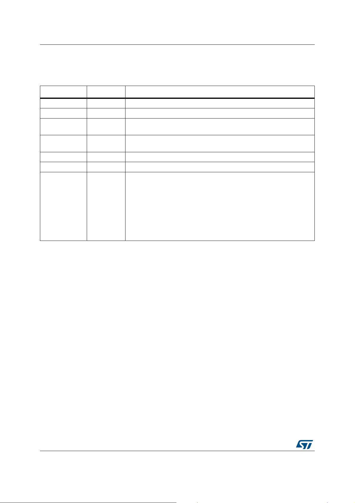
Package mechanical data L78S
7 Package mechanical data
In order to meet environmental requirements, ST offers these devices in different grades of
ECOPACK
specifications, grade definitions and product status are available at: www.st.com.
ECOPACK
®
packages, depending on their level of environmental compliance. ECOPACK®
®
is an ST trademark.
28/35 DocID2148 Rev 8
Page 29

L78S Package mechanical data
BW\SH$B5HYB7
Figure 38. TO-220 (dual gauge) drawing
DocID2148 Rev 8 29/35
35
Page 30

Package mechanical data L78S
Table 12. TO-220 (dual gauge) mechanical data
mm
Dim.
Min. Typ. Max.
A4.40 4.60
b0.61 0.88
b1 1.14 1.70
c0.48 0.70
D 15.25 15.75
D1 1.27
E 10 10.40
e2.40 2.70
e1 4.95 5.15
F1.23 1.32
H1 6.20 6.60
J1 2.40 2.72
L13 14
L1 3.50 3.93
L20 16.40
L30 28.90
∅
P3.75 3.85
Q2.65 2.95
30/35 DocID2148 Rev 8
Page 31

L78S Package mechanical data
BUHY'
Figure 39. TO-220 SG (single gauge) drawing
DocID2148 Rev 8 31/35
35
Page 32
Package mechanical data L78S
T able 13. TO-220 SG (single gauge) mechanical data
mm
Dim.
Min. Typ. Max.
A 4.40 4.60
b 0.61 0.88
b1 1.14 1.70
c 0.48 0.70
D 15.25 15.75
E 10 10.40
e 2.40 2.70
e1 4.95 5.15
F 0.51 0.60
H1 6.20 6.60
J1 2.40 2.72
L13 14
L1 3.50 3.93
L20 16.40
L30 28.90
∅
P 3.75 3.85
Q 2.65 2.95
32/35 DocID2148 Rev 8
Page 33
L78S Packaging mechanical data
8 Packaging mechanical data
Figure 40. Tube for TO-220 (dual gauge) (mm.)
Figure 41. Tube for TO-220 (single gauge) (mm.)
DocID2148 Rev 8 33/35
35
Page 34
Revision history L78S
9 Revision history
Table 14. Document revision history
Date Revision Changes
07-Sep-2006 2 Order codes updated.
20-Mar-2008 3 Added: Table 1 on page 1.
22-Mar-2010 4
08-Feb-2012 5
09-Mar-2012 6 Added: order codes L78S09CV-DG Table 13 on page 35.
15-May-2012 7 Added: order codes L78S75CV-DG and L78S10CV-DG Table 13 on page35.
10-Mar-2014 8
Added: Table 20 on page 32, Figure 38 on page33, Figure 39 on page 3 4,
Figure 40 and Figure 41 on page 33.
Added: order codes L78S05CV-DG, L78S12CV-DG and L78S15CV-DG
Table 13 on page 35.
Part numbers L78Sxx and L78SxxC changed to L78S.
Modified the title, the features and the description in cover page.
Removed TO-3 package.
Updated Table 1: Device summary, Section2: Pin configuration, Section 3:
Maximum rating s, Section 4: T est circu its, Section 5 : Electrical
characteristics,Section 6: Typical performance, Section 7: Package
mechanical data, Section 9: Order codes.
Added Section 8: Packaging mechanical data.
Minor text changes.
34/35 DocID2148 Rev 8
Page 35

L78S
Please Read Carefully:
Information in this document i s provided solely in connecti on with ST produ cts. STMicroelec troni cs NV and its subsidiari es (“ST”) res erve the
right to make changes , cor recti ons , modific ati ons or improv eme nts, t o th is doc ument, and the prod uc ts an d serv ices des crib ed he rein a t any
time, without notice.
All ST products are sold pursuant to ST’s terms and conditions of sale.
Purchasers are solely responsible for the choice, selection and use of the ST products and services described herein, and ST assumes no
liability whatsoever relating to the choice, selectio n or use of the ST products and services des cribed herein.
No license, express or implied, by estoppel or ot herwise, to any intellectual property rights is granted under this document. I f any part of this
document refers to any third party products or services it shall not be deemed a license grant by ST for the use of such third party products
or services, or any intellectual property contained therein or considered as a warranty covering the use in any manner whatsoever of such
third party products or services or any intellectual property contained therein.
UNLESS OTHERWISE SET FORTH IN ST’S TERMS AND CONDITIONS OF SALE ST DISCLAIMS ANY EXPRESS OR IMPLIED
WARRANTY WITH RESPECT TO THE USE AND/OR SALE OF ST PRODUCTS INCLUDING WITHOUT LIMITATION IMPLIED
WARRANTIES OF MERCHANTABILITY, FITNESS FOR A PARTICULAR PURPOSE (AND THEIR EQUIVALENTS UNDER THE LAWS
OF ANY JURISDICTION), OR INFRINGEMENT OF ANY PATENT, COPYRIGHT OR OTHER INTELLECTUAL PROPERTY RIGHT.
ST PRODUCTS ARE NOT DESIGNED OR AUTHORIZED FOR USE IN: (A) SAFETY CRITICAL APPLICATIONS SUCH AS LIFE
SUPPORTING, ACTIVE IMPLANTED DEVICES OR SYSTEMS WITH PRODUCT FUNCTIONAL SAFETY REQUIREMENTS; (B)
AERONAUTIC APPLICATIONS; (C) AUTOMOTIVE APPLICATIONS OR ENVIRONMENTS, AND/OR (D) AEROSPACE APPLICATIONS
OR ENVIRONMENTS. WHERE ST PRODUCTS ARE NOT DESIGNED FOR SUCH USE, THE PURCHASER SHALL USE PRODUCTS AT
PURCHASER’S SOLE RISK, EVEN IF ST HAS BEEN INFORMED IN WRITING OF SUCH USAGE, UNLESS A PRODUCT IS
EXPRESSLY DESIGNATED BY ST AS BEING INTENDED FOR “AUTOMOTIVE, AUTOMOTIVE SAFETY OR MEDICAL” INDUSTRY
DOMAINS ACCORDING TO ST PRODUCT DESIGN SPECIFICATIONS. PRODUCTS FORMALLY ESCC, QML OR JAN QUALIFIED ARE
DEEMED SUITABLE FOR USE IN AEROSPACE BY THE CORRESPONDING GOVERNMENTAL AGENCY.
Resale of ST products with prov isions differen t from the state ments and/or tec hnical featur es set forth in th is document shall immediatel y void
any warranty granted by ST for the ST product or service described herein and shall not create or extend in any manner whatsoever, any
liability of ST.
ST and the ST logo are trademark s or registered trademarks of ST in various countries.
Information in this document supers edes and replaces all information previously supplied.
The ST logo is a registered trademark of STMicroelectronics. All other names are the property of their respective owners.
© 2014 STMicroelectronics - All rights reserv ed
STMicroelectronics group of companies
Australia - Belgium - Brazil - Canada - China - Czech Republic - Finland - France - Germany - Hong Kong - India - Israel - Italy - Japan -
Malaysia - Malta - Morocco - Philippines - Si ngapore - Spain - Sweden - Switzerland - United Kin gdom - United States of America
www.st.com
DocID2148 Rev 8 35/35
35
 Loading...