

STMicroelectronics TSH80, TSH81, TSH82 Technical data
Wide Band, Rail-to-Rail Operational Amplifier
■ 4.5V, 12V operating conditions
■ 3dB-bandwidth: 100MHz
■ Slew-rate: 100V/µs
■ Output current: up to 55mA
■ Input single supply voltage
■ Output rail-to-rail
■ Specified for 150Ω load
■ Low distortion, THD: 0.1%
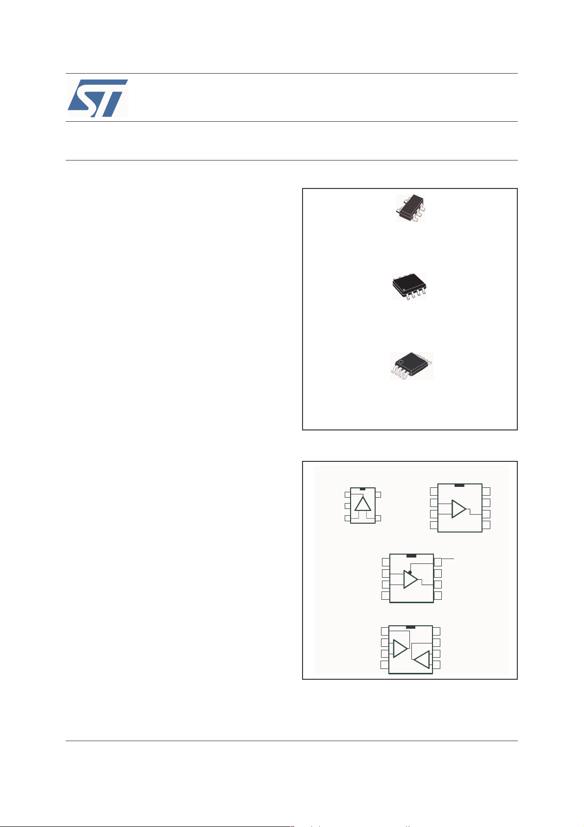
■ SOT23-5, TSSOP and SO packages
Description
The TSH8x series offers single and dual
operational amplifiers featuring high video
performances with large bandwidth, low distortion
and excellent supply voltage rejection. These
amplifiers feature also large output voltage swing
and high output current capability to drive
standard 150Ω loads.
TSH80-TSH81-TSH82
with Standby Function
L
SOT23-5
(Plastic Micro package)
D
SO-8
(Plastic Micro package)
P
TSSOP8
(Plastic Micro package)
Running at single or dual supply voltage from
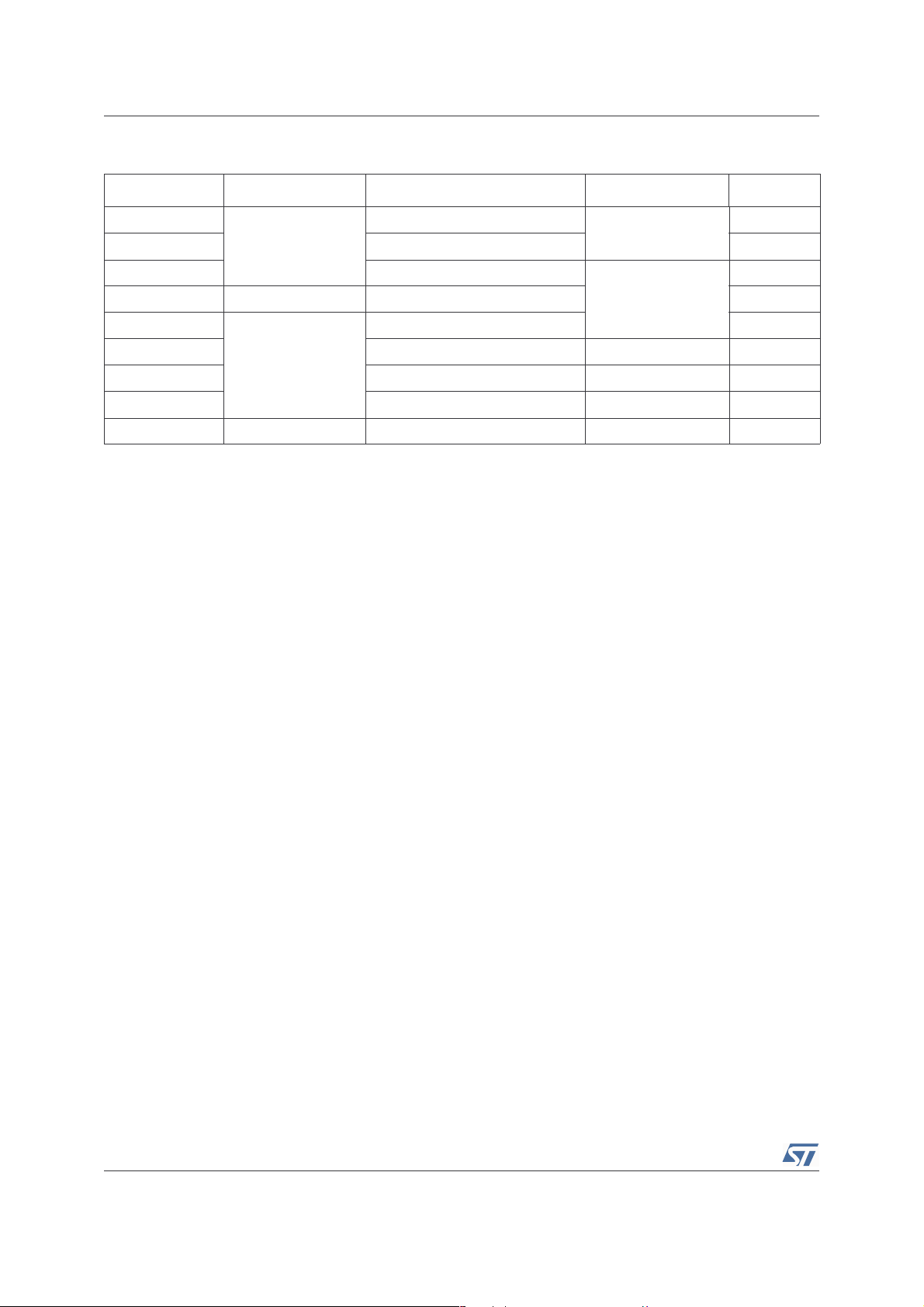
Pin Connections (top view)
4.5V to 12V, these amplifiers are tested at
5V(±2.5V) and 10V(±5V) supplies.
Output
The TSH81 also features a standby mode, which
allows the operational amplifier to be put into a
standby mode with low power consumption and
Output
VCC -
VCC -
Non-Inv. In.
Non-Inv. In.
high output impedance.The function allows power
saving or signals switching/multiplexing for high
speed applications and video applications.
For board space and weight saving, TSH8x series
is proposed in SOT23-5, TSSOP8 and SO-8
Non Inverting Input
Non Inverting Input
packages.
Application
■ Video buffers
■ A/D converters driver
■ Hi-Fi applications
August 2005 1/23
Non Inve rting Input1
Non Inve rting Input1
TSH80 : SOT23-5/SO8
TSH80 : SOT23-5/SO8
NC
NC
1
1
1
2
2
3
3
Inverting Input
Inverting Input
Inverting Input1 Output2
Inverting Input1 Output2
5
5
VCC +
VCC +
+ -
+ -
TSH81 : SO8/TSSOP8
TSH81 : SO8/TSSOP8
VCC -
VCC -
TSH82 : SO8/TSSOP8
TSH82 : SO8/TSSOP8
Output1
Output1
VCC -
VCC -
Non-Inv. I n.
Non-Inv. I n.
Inv. In.
Inv. In.
4
4
NC
NC
1
1
2
2
3
3
1
1
2
2
_
_
+
+
3
3
1
2
2
Inv. In.
Inv. In.
3
3
VCC -
VCC -
8
8
STANDBY
STANDBY
_
_
+
+
7
7
VCC +
VCC +
Output
Output
6
6
NC
NC
54
54
VCC +
VCC +
8
8
7
7
Inverting Input2
Inverting Input2
_
_
6
6
+
+
Non Inv erting I nput2
Non Inv erting I nput2
54
54
_
_
+
+
NC
NC
8
8
7
7
VCC +
VCC +
Output
Output
6
6
NC
NC
54
54
Rev 2
www.st.com
23
TSH80-TSH81-TSH82
Order Codes
Type Temperature Range Package Packaging Marking
TSH80ILT
TSH80IYLT SOT23-5 (automotive grade level) K310
TSH80ID/DT SO-8
TSH80IYD/IYDT -40°C to +125°C SO-8 (automotive grade level) SH80IY
TSH81ID/DT
TSH81IPT TSSOP8 Tape & Reel SH81I
TSH82ID/DT SO-8 Tube or Tape & Reel TSH82I
TSH82IPT TSSOP8 Tape & Reel SH82I
TSH82IYD/ITDT -40°C to +125°C SO-8 (automotive grade level) Tube or Tape & Reel SH82IY
-40°C to +85°C
-40°C to +85°C
SOT23-5
Tape & Reel
Tube or Tape & Reel
SO-8 TSH81I
K303
TSH80I
2/23
TSH80-TSH81-TSH82 Absolute Maximum Ratings
1 Absolute Maximum Ratings
Table 1. Key parameters and their absolute maximum ratings
Symbol Parameter Value Unit
(3)
(1)
(2)
14 V
±2V
±6V
(4)
80
28
37
V
CC Supply Voltage
T
V
T
id
V
oper
stg
T
Differential Input Voltage
Input Voltage
i
Operating Free Air Temperature Range -40 to +85 °C
Storage Temperature -65 to +150 °C
Maximum Junction Temperature 150 °C
j
Thermal resistance junction to case
R
thjc
SOT23-5
SO8
TSSOPO8
Thermal resistance junction to ambient area
R
thja
SOT23-5
SO8
TSSOPO8
250
157
130
ESD Human Body Model 2 kV
1. All voltage values, except differential voltage are with respect to network ground terminal
2. Differential voltages are non-inverting input terminal with respect to the inverting terminal
3. The magnitude of input and output must never exceed VCC +0.3V
4. Short-circuits can cause excessive heating
°C/W
°C/W
Table 2. Operating conditions
Symbol Parameter Value Unit
V
V
Standby
Supply Voltage 4.5 to 12 V
CC
Common Mode Input Voltage Range
IC
-
V
to (V
CC
-
) to (V
(V
CC
CC
+
-1.1)
CC
+
)
V
V
3/23
Electrical Characteristics TSH80-TSH81-TSH82
2 Electrical Characteristics
Table 3. V
CC
+
= +5V, V
-
= GND, Vic = 2.5V, T
CC
= 25°C (unless otherwise specified)
amb
Symbol Parameter Test Condition Min. Typ. Max. Unit
|V
∆V
C
I
T
|
Input Offset Voltage
io
Input Offset Voltage Drift vs.
io
Temperature
I
Input Offset Current
io
I
Input Bias Current
ib
Input Capacitance 0.3 pF
in
Supply Current per Operator
CC
T
T
T
T
T
T
T
T
amb
min.
min.
amb
min.
amb
min.
amb
min.
< T
amb
< T
amb
= 25°C
< T
amb
= 25°C
< T
amb
= 25°C
< T
amb
< T
< T
< T
< T
< T
max.
max.
max.
max.
max.
1.1 10
12
3 µV/°C
0.1 3.5
5
615
20
8.2 10.5
11.5
= 25°C
+0.1<Vic<3.9V &
CMR
SVR
PSR
Common Mode Rejection Ratio
(δVic/δVio)
Supply Voltage Rejection Ratio
(δVcc/δVio)
Power Supply Rejection Ratio
(δVcc/δVou t )
Vout=2.5V
T
= 25°C
amb
T
< T
min.
= 25°C
T
amb
T
< T
min.
amb
amb
< T
< T
max.
max.
727097 dB
686575
Positive & Negative Rail 75 dB
mV
µA
µA
mA
dB
A
Large Signal Voltage Gain
vd
Output Short Circuit Current
I
o
Source
4/23
=150Ω to 1.5V
R
L
V
=1V to 4V
out
T
= 25°C
amb
T
< T
min.
amb
=25°C
T
amb
V
=+1, V
id
V
id
=-1, V
out
out
|Source|
Sink
T
< T
min.
amb
Vid=+1, V
V
id
=-1, V
out
out
|Source|
Sink
< T
max.
to 1.5V
to 1.5V
< T
max.
to 1.5V
to 1.5V
757084
55
35
55
33
28
28
dB
mA
TSH80-TSH81-TSH82 Electrical Characteristics
Table 3. V
CC
+
= +5V, V
-
= GND, Vic = 2.5V, T
CC
= 25°C (unless otherwise specified)
amb
Symbol Parameter Test Condition Min. Typ. Max. Unit
T
=25°C
amb
R
= 150Ω to GND
L
R
= 600Ω to GND
L
R
= 2kΩ to GND
L
R
= 10kΩ to GND
L
R
= 150Ω to 2.5V
V
High Level Output Voltage
oh
L
R
= 600Ω to 2.5V
L
R
= 2kΩ to 2.5V
L
R
= 10kΩ to 2.5V
L
< T
T
min.
amb
< T
max.
RL = 150Ω to GND
R
= 150Ω to 2.5V
L
T
=25°C
amb
R
= 150Ω to GND
L
R
= 600Ω to GND
L
R
= 2kΩ to GND
L
R
= 10kΩ to GND
L
4.2
4.5
4.1
4.4
4.36
4.85
4.90
4.93
4.66
4.90
4.92
4.93
48
54
55
56
150
V
400
= 150Ω to 2.5V
R
V
Low Level Output Voltage
ol
L
R
= 600Ω to 2.5V
L
R
= 2kΩ to 2.5V
L
R
= 10kΩ to 2.5V
L
< T
T
min.
amb
< T
max.
RL = 150Ω to GND
R
= 150Ω to 2.5V
L
220
105
76
61
mV
200
450
F=10MHz
A
GBP Gain Bandwidth Product
Bw Bandwidth @-3dB
SR Slew Rate
φm Phase Margin
=+11
VCL
A
=-10
VCL
A
=+1
VCL
R
=150Ω to 2.5V
L
=+2
A
VCL
R
=150Ω // CL to 2.5V
L
C
= 5pF
L
C
= 30pF
L
R
=150Ω // 30pF to 2.5V
L
65
55
87 MHz
104
60
105
40 °
MHz
V/µs
en Equivalent Input Noise Voltage F=100kHz 11 nV/√Hz
A
=+2, F=4MHz
VCL
R
=150Ω // 30pF to 2.5V
THD Total Harmonic Distortion
V
V
L
out
out
=1Vpp
=2Vpp
-61
-54
dB
5/23
Electrical Characteristics TSH80-TSH81-TSH82
Table 3. V
CC
+
= +5V, V
-
= GND, Vic = 2.5V, T
CC
= 25°C (unless otherwise specified)
amb
Symbol Parameter Test Condition Min. Typ. Max. Unit
A
IM2
Second order inter modulation
product
=+2, V
VCL
R
=150Ω to 2.5V
L
Fin1=180kHz,
Fin2=280kHz
out
=2Vpp
-76 dBc
spurious measurement
@100kHz
A
IM3
Third order inter modulation
product
=+2, V
VCL
R
=150Ω to 2.5V
L
Fin1=180kHz,
Fin2=280KHz
out
=2Vpp
-68 dBc
spurious measurement
@400kHz
A
=+2, RL=150Ω to
VCL
∆G Differential gain
Df Differential phase
Gf Gain Flatness
2.5V
F=4.5MHz, V
=+2, RL=150Ω to
A
VCL
out
2.5V
F=4.5MHz, V
out
F=DC to 6MHz, A
=2Vpp
=2Vpp
VCL
=+2
0.5 %
0.5 °
0.2 dB
Vo1/Vo2 Channel Separation F=1MHz to 10MHz 65 dB
Table 4. V
CC
+
= +5V, V
-
= -5V, Vic = GND, T
CC
= 25°C (unless otherwise specified)
amb
Symbol Parameter Test Condition Min. Typ. Max. Unit
|V
∆V
C
I
T
|
Input Offset Voltage
io
Input Offset Voltage Drift vs.
io
Temperature
I
Input Offset Current
io
I
Input Bias Current
ib
Input Capacitance 0.7 pF
in
Supply Current per Operator
CC
T
T
T
T
T
T
T
T
amb
min.
min.
amb
min.
amb
min.
amb
min.
< T
amb
< T
amb
= 25°C
< T
amb
= 25°C
< T
amb
= 25°C
< T
amb
< T
< T
< T
< T
< T
max.
max.
max.
max.
max.
0.8 10
12
2 µV/°C
0.1 3.5
5
615
20
9.8 12.3
13.4
= 25°C
-4.9 < Vic < 3.9V &
CMR
SVR
Common Mode Rejection Ratio
(δVic/δVio)
Supply Voltage Rejection Ratio
(δVCC/δVio)
Vout=GND
T
= 25°C
amb
T
< T
min.
= 25°C
T
amb
T
< T
min.
amb
amb
< T
< T
8172106 dB
max.
716577
max.
mV
µA
µA
mA
dB
6/23
TSH80-TSH81-TSH82 Electrical Characteristics
Table 4. V
CC
+
= +5V, V
-
= -5V, Vic = GND, T
CC
= 25°C (unless otherwise specified)
amb
Symbol Parameter Test Condition Min. Typ. Max. Unit
PSR
A
V
Power Supply Rejection Ratio
(δVCC/δVout )
Large Signal Voltage Gain
vd
Output Short Circuit Current
I
o
Source
High Level Output Voltage
oh
Positive & Negative Rail 75 dB
=150Ω to GND
R
L
V
=-4 to +4
out
T
= 25°C
amb
T
< T
min.
amb
T
=25°C
amb
V
=+1, V
id
V
id
=-1, V
out
out
|Source|
Sink
T
< T
min.
amb
Vid=+1, V
V
id
=-1, V
out
out
|Source|
Sink
T
=25°C
amb
R
= 150Ω to GND
L
R
= 600Ω to GND
L
R
= 2kΩ to GND
L
R
= 10kΩ to GND
L
< T
max.
to 1.5V
to 1.5V
< T
max.
to 1.5V
to 1.5V
757086
35
30
28
28
4.2
4.36
4.85
4.9
4.93
55
55
dB
mA
V
V
Low Level Output Voltage
ol
GBP Gain Bandwidth Product
Bw Bandwidth @-3dB
SR Slew Rate
φmPhase Margin
T
< T
amb
< T
max.
min.
RL = 150Ω to GND
T
=25°C
amb
R
= 150Ω to GND
L
R
= 600Ω to GND
L
R
= 2kΩ to GND
L
R
= 10kΩ to GND
L
T
< T
amb
< T
max.
min.
RL = 150Ω to GND
F=10MHz
A
=+11
VCL
=-10
A
VCL
=+1
A
VCL
R
=150Ω // 30pF to GND
L
=+2
A
VCL
R
=150Ω // CL to GND
L
C
= 5pF
L
C
= 30pF
L
R
=150Ω to gnd
L
4.1
-4.63
-4.86
-4.9
-4.93
65
55
100 MHz
117
68
118
40 °
-4.4
mV
-4.3
MHz
V/µs
7/23
 Loading...