

Page 1
TSH341
300MHz Single Supply Video Amplifier with Low In/Out Rail
■ Bandwidth: 300MHz
■ Single supply operation down to 3V
■ Low input & output rail
■ Very low harmonic distortion
■ Slew rate: 400V/µs
■ Voltage Input noise: 7nV/√Hz
■ Specified for 150Ω load and 100Ω load
■ Tested on 5V power supply
■ Data min. and max. are tested during
production (Table 3)
Description
The TSH341 is a single supply operational
amplifier featurin g a large bandwidth of 300MHz
at unity gain for only 9.8mA of quiescent current.
An advantage of this circuit is its low input and
output rail feature wh ich is very close to GND in
single supply. This rail is tested and guaranteed
during production at 60mV (max.) from G ND on a
Ω load. This allows a good output swing which
150
fits perfectly when driving a video signal on a 75Ω
video line. Chapter 5 gives technical support
when using the TSH341 as a driver for video DAC
output on a video line . In particular, this chapter
focuses on applying a video signal DC shift to
avoid any clamping of the synchronization tip.
The TSH341 is available in the tiny SOT23-5 and
SO8 plastic packages.
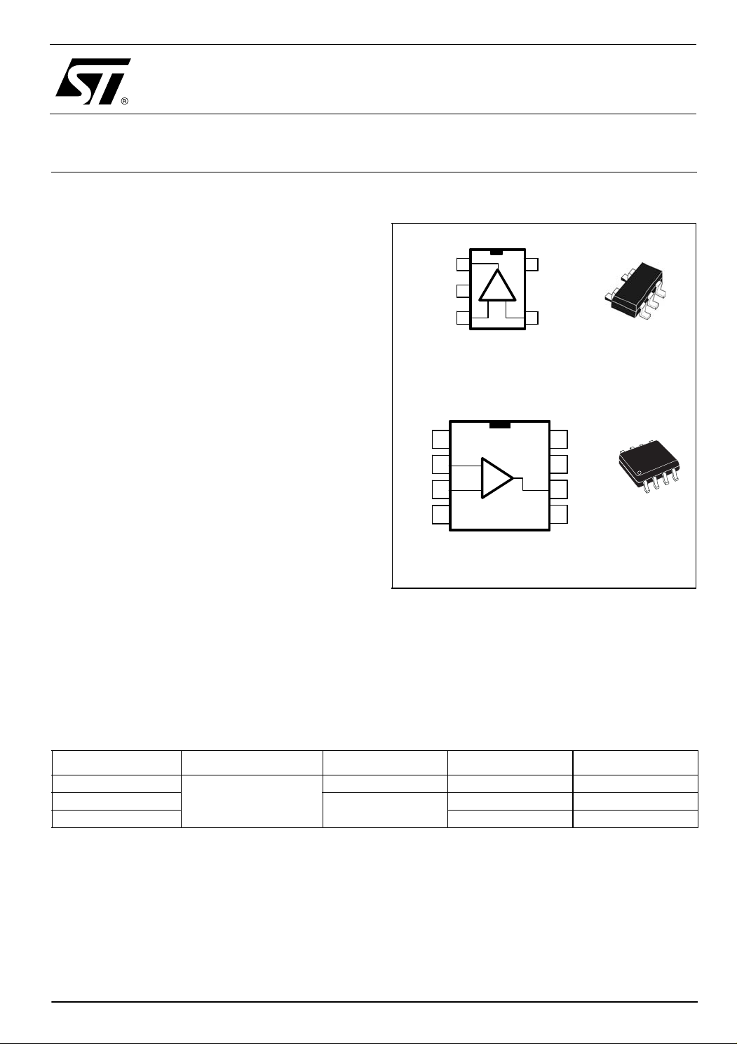
Pin Connections (top view)
OUT
OUT
NC
NC
-IN
-IN
+IN
+IN
-VCC
-VCC
-VCC
-VCC
1
1
2
2
3
3
4
4
1
1
2
2
3
3
SOT23-5
SOT23-5
+ -
+ -
_
_
+
+
SO8
SO8
5
5
4
4
+VCC
+VCC
-IN+IN
-IN+IN
8
8
7
7
6
6
5
5
NC
NC
+VCC
+VCC
OUT
OUT
NC
NC
Applications
■ High-end video systems
■ High Definition TV (HDTV)
■ Broadcast video
■ Multimedia products
Order Codes
Part Number Temperature Range Package Packaging Marking
TSH341ILT
TSH341ID
TSH341IDT Tape & Reel H341I
March 2005 Revision 2 1/13
-40°C to +85°C
SOT23-5 Tape & Reel K307
SO-8
Tube H341I
Page 2
TSH341 Absolute Maximum Ratings
1 Absolute Maximum Ratings
Table 1. Key parameters and their absolute maximum ratings
Symbol Parameter Value Unit
V
CC
Vid
V
in
T
oper
T
std
T
R
thjc
R
thja
P
max.
ESD
Supply voltage
Differential Input Voltage
Input Voltage Range
Operating Free Air Temperature Range
Storage Temperature
Maximum Junction Temperature
j
Thermal Resistance Junction to Case
SOT23-5
SO8
Thermal Resistance Junction to Ambient Area
SOT23-5
SO8
Maximum Power Dissipation (@Ta=25°C) for Tj=150°C
SOT23-5
SO8
CDM: Charged Device Model
HBM: Human Body Model
MM: Machine Model
Output Short Circuit
1
2
3
6V
+/-0.5 V
-0.2 to +3 V
-40 to +85 °C
-65 to +150 °C
150 °C
80
°C/W
28
250
°C/W
175
500
mW
715
2
1.5
200
4
kV
kV
V
1) All voltage values, except different ial voltage are with respect to network terminal.
2) Differential voltage are non-invert ing input terminal with respect to the inverting input terminal.
3) The magnitude of input and output voltage must never exceed VCC +0.3V.
4) An output current limitation protects the circuit from trans ient currents. Short-circuits can cause excessive heati ng.
Destructive dissipation can result from short circuit on amplifiers.
Table 2. Operating conditions
Symbol Parameter Value Unit
V
Power Supply Voltage
CC
Vicm Common Mode Input Voltage -0.4 to 3 V
1) Tested in full production at 0V/5V single power supply
3 to 5.5
1
V
2/13
Page 3
Electrical Characteristics TSH341
2 Electrical Characteristics
Table 3. V
= +5V, T
CC
= 25°C (unless otherwise specified)
amb
Symbol Parameter Test Condition Min. Typ. Max. Unit
DC Performance
V
io
∆V
I
ib
A
VD
CMR
SVR
PSR
R
IN
C
IN
CC
I
Input Offset Voltage T
Vio drift vs. Temperature -40°C < T
io
Input Bias Current T
Open Loop Gain ∆V
Common Mode Rejection Ratio
20 log (∆V
icm
/∆Vio)
Supply Voltage Rejection Ratio
20 log (∆V
/∆Vio)
cc
Power Supply Rejection Ratio
/∆V
20 log (∆V
)
cc
out
Input Resistance
Input Capacitance
Total Supply Current No Load, V
, V
amb
-40°C < T
amb
-40°C < T
∆V
-40°C < T
∆V
-40°C < T
∆V
=0.6V
icm
< +85°C
amb
< +85°C
amb
, V
=0.6V
icm
< +85°C
amb
=2V, RL=150Ω
OUT
= 2V
icm
< +85°C
amb
=4V to 5V, V
cc
< +85°C
amb
=200mVp-p, F=1MHz
cc
=0.6V
icm
icm
=0.6V
-15 -3 15
-5
-30 µV/°C
616
7.2
70 100 dB
-60 -85
-83
-60 -85
-84
-77 dB
8.2 MΩ
3.5 pF
9.8 12.7 mA
Dynamic Performance and Output Characteristics
OUT
OUT
=0.6V,
icm
= 2Vp-p,
OUT
= 150Ω
L
< +85°C
=20mVp
=20mVp
300
90
150
MHz
65
70 100 MHz
400 V/µs
3.7 3.9 V
40 60 mV
70 100
90
Bw
FPBW
SR
V
OH
V
OL
I
OUT
-3dB Bandwidth Small Signal V
=0.6V, RL=150Ω
V
icm
Gain=+1
Gain=+2
Gain Flatness @ 0.1dB Small Signal V
Gain=+2, V
L=150Ω
R
Full Power Bandwidth V
icm
=2V, V
Gain=1, R
Slew Rate V
=2Vp-p, RL=150Ω,
OUT
Gain=+2,
High Level Output Voltage RL = 150Ω
Low Level Output Voltage RL = 150Ω
Output Short Circuit Current T
amb
-40°C < T
amb
Noise and Distortion
eN Equivalent Input Noise Voltage F = 100kHz 7 nV/√Hz
iN Equivalent Input Noise Current (+) F = 100kHz 1.5 pA/√Hz
HD2
HD3
2nd Harmonic Distortion V
3rd Harmonic Distortion V
= 2Vp-p, RL = 150Ω
OUT
Gain=+2, F= 10MHz,
= 2Vp-p, RL = 150Ω
OUT
Gain=+2, F= 10MHz,
-57 dBc
-63 dBc
mV
µA
dB
dB
mA
3/13
Page 4
TSH341 Electrical Characteristics
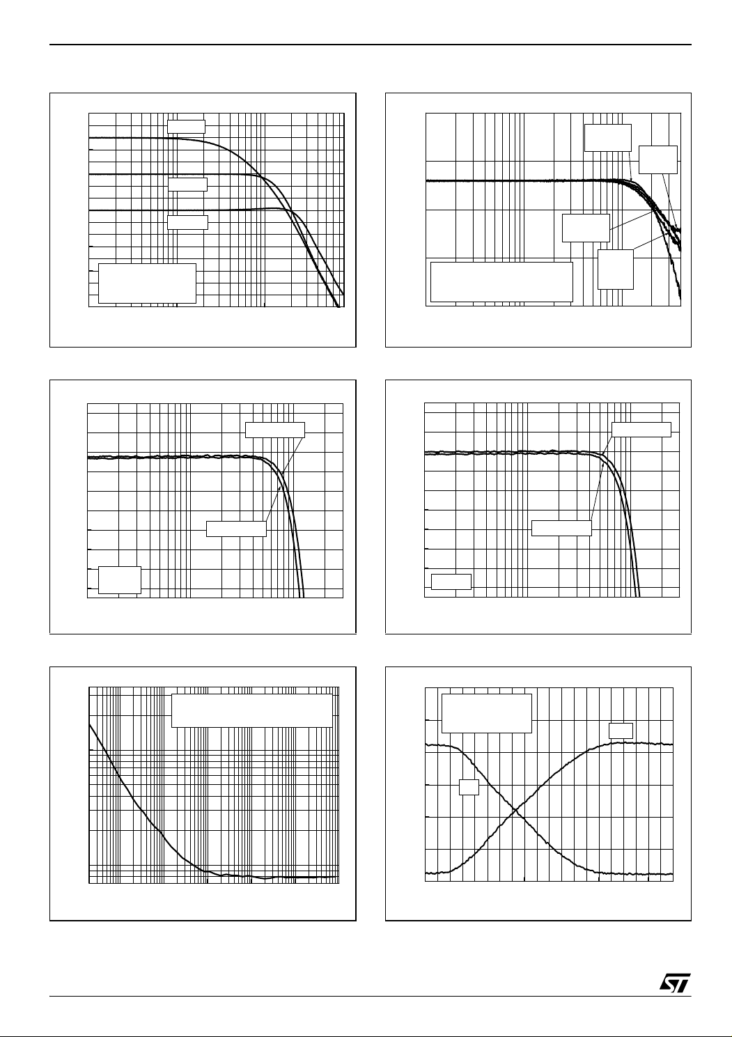
Figure 1. Frequency response
16
14
12
10
8
6
4
2
0
-2
Gain (dB)
-4
-6
-8
-10
Vcc=5V
-12
Load=100
-14
SO8 and SOT23-5
-16
1M 10M 100M
Gain=+4
Gain=+2
Gain=+1
Ω or 150Ω
Frequency (Hz)
Figure 2. Gain flatness - SOT23-5L
6,4
6,2
6,0
5,8
5,6
5,4
Gain (dB )
5,2
5,0
4,8
Vcc=5V
Gain=+2
4,6
1M 10M 100M
Frequency (Hz)
Load=150Ω
Load=100Ω
Figure 4. Frequency response on capa-load
20
C=47pF
Ω
Riso=10
10
0
C=10pF
Riso=0
C=22pF
Ω
Riso=10
-10
Vcc=5V
Frequency Response (dB)
Gain=+2
Load=Riso + C//1k
-20
1M 10M 100M
Ω (to ground)
C=0 or
10pF
Riso=0
Frequency (Hz)
Figure 5. Gain flatness - SO8
6,4
6,2
6,0
5,8
5,6
5,4
Gain (dB)
5,2
5,0
4,8
Vcc=5V
4,6
1M 10M 100M
Load=100Ω
Frequency (Hz)
Load=150Ω
Figure 3. T otal input noise vs. frequency
non-inverting input in short-circuit
Vcc=5V
100
Input Noise (nV/VHz)
10
100 1k 10k 100k 1M 10M
Frequency (Hz)
4/13
Figure 6. Positive and negative slew rate
3,0
Vcc=5V
G=+2
2,5
Load=100
Ω or 150Ω
2,0
1,5
1,0
SR-
Output Response (V)
0,5
0,0
-5ns -4ns -3ns -2ns -1ns 0s 1ns 2ns 3ns 4ns 5ns
Time
SR+
Page 5

Electrical Characteristics TSH341
HD2 & HD3 (dBc)
HD2 & HD3 (dBc)
0
Figure 7. Distortion on 100Ω load
HD2
(10MHz)
Vcc=5V
Load=100
-20
-25
-30
-35
-40
-45
-50
-55
-60
-65
-70
-75
-80
-85
-90
01234
HD3
(30MHz)
HD2
(30MHz)
HD3
(10MHz)
Output Amplitude (Vp-p)
Figure 8. Output lower rail vs. frequency
500
Vcc=5V
Load=100
400
300
(mV)
OL
200
V
100
0
10k 100k 1M 10M 100M
Ω or 150Ω
Frequency (Hz)
Figure 10. Distortion on 150Ω load
HD2
(30MHz)
HD2
(10MHz)
Vcc=5V
Load=150
Ω
-10
-15
-20
-25
-30
-35
-40
-45
-50
-55
-60
-65
-70
Ω
-75
-80
01234
HD3
(30MHz)
HD3
(10MHz)
Output Amplitude (Vp-p)
Figure 11. Output voltage swing vs. Vcc
5
4
3
2
Vout max (Vp-p)
1
F=30MHz
Load=100
0
3,00 3,25 3,50 3,75 4,00 4,25 4,50 4,75 5,00
Ω or 150Ω
Vcc (V)
Figure 9. Output voltage swing vs. frequency
5
Figure 12. Quiescent current vs. Vcc
20
no load
Vout max. (Vp-p)
4
3
2
1
Vcc=5V
15
10
Icc (mA)
5
Gain=+2
Load=100
0
Ω or Load=150Ω
1M 10M
Frequency (Hz)
0
1,5 2,0 2,5 3,0 3,5 4,0 4,5 5,
Vcc (V)
5/13
Page 6

TSH341 Electrical Characteristics
0
Vio (mV)
Figure 13. Isource
0
-10
-20
-30
-40
+3V
-50
-60
-70
Isource (mA)
-80
-90
-100
-110
-120
0,0 0,5 1,0 1,5 2,0 2,5 3,0 3,5 4,0 4,5 5,
+5V
VOH
without loa d
Isource
V
0V
V (V)
Figure 14. Bandwidth vs. temperature
300
250
Figure 16. Reverse isolation vs. frequency
0
-20
-40
-60
Gain (dB )
-80
Small Signal
Vcc=5V
Load=100
-100
1M 10M 100M 1G
Ω
Frequency (Hz)
Figure 17. Ibias vs. temperature
11,0
10,5
10,0
200
Bw (MHz)
150
Vcc=5V
Gain=+1
Load=150
100
-40-200 20406080
Ω
Temperature (°C)
Figure 15. Input offset vs. temperature
0
-1
-2
-3
-4
Vcc=5V
Load=150
-5
-40-200 20406080
Ω
Temperature (°C)
9,5
(µA)
BIAS
I
9,0
8,5
Vcc=5V
Load=150
Ω
8,0
-40-200 20406080
Temperature (°C)
Figure 18. Supply current vs. temperature
12
11
10
(mA)
CC
I
9
8
Vcc=5V
no Load
7
-40-200 20406080
Temperature (°C)
6/13
Page 7

Electrical Characteristics TSH341
V
(V)
Figure 19. Output lower rail vs. temperature
0,10
Vcc=5V
Gain=+2
0,08
Load=150
Ω
0,06
(V)
OL
V
0,04
0,02
0,00
-40-200 20406080
Temperature (°C)
Figure 20. SVR vs. temperature
86,0
85,8
85,6
85,4
85,2
85,0
84,8
SVR (dB)
84,6
84,4
84,2
Vcc=5V
84,0
-40-20 0 20406080
Temperature (°C)
Figure 21. Output higher rail vs. temperature
4,50
4,25
4,00
OH
3,75
Vcc=5V
Gain=+2
Load=150
3,50
-40-200 20406080
Ω
Temperature (°C)
Figure 22. CMR vs. temperature
88
86
84
CMR (dB)
82
Vcc=5V
80
-40-20 0 20406080
Temperature (°C)
7/13
Page 8

TSH341 Evaluation Boards
3 Evaluation Boards
An evaluation board kit optimized for high speed operational amplifiers is available (order code:
KITHSEVAL/STDL). T he kit includes t he following evaluation boards, as well as a CD-ROM containing
datasheets, articles, application notes and a user manual:
z SOT23_SINGLE_HF BOARD: B oard for the eval uation of a singl e high-speed op-amp in SOT23-5
package.
z SO8_SINGLE_HF: Board for the evaluation of a single high-speed op-amp in SO8 package.
z SO8_DUAL_HF: Board for the evaluation of a dual high-speed op-amp in SO8 package.
z SO8_S_MULTI: Board for the evaluation of a single high-speed op-amp in SO8 package in inverting
and non-inverting configuration, dual and signle supply.
z SO14_TRIPLE: Board for the eval uation of a tri ple h igh-spe ed op -amp in SO 14 pack age with vide o
application considerations.
Board material:
z 2 layers
z FR4 (εr=4.6)
z epoxy 1.6mm
z copper thickness: 35µm
Figure 23: Evaluation kit for high speed op-amps
8/13
Page 9

Power Supply Considerations TSH341
4 Power Supply Considerations
Correct power supply bypassin g is very impor tant for optimi zing performa nce in high -frequency r anges.
Bypass capacitors should be placed as close as possible to the IC pins to improve high-frequency
bypassing. A capacitor greater than 10µF is necessary to minimize the distortion. For better quality
bypassing, a capacit or of 10nF is added using the sam e implementation cond itions. Bypass capacito rs
must be incorporated for both the negative and the positive supply. On the SO8_SINGLE_HF board,
these capacitors are C8 and C6.
Figure 24: Circuit for power supply bypassing
+VCC
+
+
_
_
+VCC
10nF
10nF
TSH341
TSH341
GND
GND
+V
+V
10microF
10microF
+
+
CC
CC
9/13
Page 10

TSH341 Using the TSH341 to Drive Video Signals
5 Using the TSH341 to Drive Video Signals
Figure 25. Implementation of the video driver on output video DACs
Volt
Volt
+5V
Rg
Rg
+
+
_
_
+5V
Rfb
Rfb
Video
Video
DAC
DAC
1Vpp
1Vpp1Vpp
Reconstruction
Reconstruction
Filtering
Filtering
LPF
LPF
VOL(50MHz) = 150mV (Figure 8)
To drive the video signal properl y, the output of the driver must be at least equal to
250mV (assuming V
z 1st solution:
and VOL variations).
io
Set the video DAC 0-IRE output level to 125mV.
Video
Video
Signal
Signal
2.250V
2.250V
250mV
250mV
time
time
2Vpp
2Vpp
75Ω
75Ω
Volt
Volt
Volt
75Ω Cable
75Ω Cable
Video
Video
Signal
Signal
1.125V
1.125V
1.125V
1.125V
125mV
125mV
125mV
125mV
time
time
time
time
1Vpp
1Vpp1Vpp
75Ω
75Ω
100 IRE
White Level
White Level
Black Level
Black Level
z 2nd solution:
100 IRE
30 IRE
30 IRE
0 IRE
0 IRE
300mV
300mV
SynchronizationTip
SynchronizationTip
Image Content
Image Content
150mV
150mV
0V
0V
Implementation of a DC component in the input of the driver.
Volt
Video
Video
DAC
DAC
DC component
DC component
33uF
33uF
1Vpp
1Vpp1Vpp
=125mV
=125mV
Reconstruction
Reconstruction
Filtering
Filtering
LPF
LPF
1k
1k
+5V
+5V
+
+
_
_
Rg
Rg
Volt
Rfb
Rfb
Video
Video
Signal
Signal
2.250V
2.250V
250mV
250mV
time
time
1Vp-p
1Vp-p
75Ω
75Ω
2Vpp
2Vpp
Volt
Volt
Volt
75Ω Cable
75Ω Cable
Video
Video
Signal
Signal
1.125V
1.125V
1.125V
1.125V
125mV
125mV
125mV
125mV
time
time
time
time
1Vpp
1Vpp1Vpp
75Ω
75Ω
10/13
Page 11

Package Mechanical Data TSH341
6 Package Mechanical Data
6.1 SO-8 Package
SO-8 MECHANICAL DATA
DIM.
A 1.35 1.75 0.053 0.069
A1 0.10 0.25 0.04 0.010
A2 1.10 1.65 0.043 0.065
B 0.33 0.51 0.013 0.020
C 0.19 0.25 0.007 0.010
D 4.80 5.00 0.189 0.197
E 3.80 4.00 0.150 0.157
e 1.27 0.050
H 5.80 6.20 0.228 0.244
h 0.25 0.50 0.010 0.020
L 0.40 1.27 0.016 0.050
k ˚ (max.)
ddd 0.1 0.04
MIN. TYP MAX. MIN. TYP. MAX.
mm. inch
8
0016023/C
11/13
Page 12

TSH341 Package Mechanical Data
6.2 SOT23-5L (5-pin) package
SOT23-5L MECHANICAL DATA
DIM.
MIN. TYP MAX. MIN. TYP. MAX.
A 0.90 1.45 35.4 57.1
A1 0.00 0.15 0.0 5.9
A2 0.90 1.30 35.4 51.2
b 0.35 0.50 13.7 19.7
C 0.09 0.20 3.5 7.8
D 2.80 3.00 110.2 118.1
E 2.60 3.00 102.3 118.1
E1 1.50 1.75 59.0 68.8
e.95 37.4
e1 1.9 74.8
L 0.35 0.55 13.7 21.6
mm. mils
0
12/13
Page 13

TSH341
7 Revision History
Date Revision Description of Changes
01 Jan. 2005 1 First release corresponding to Preliminary Data version of datasheet.
23 Mar. 2005 2 Datasheet of mature, full-specification product
Information furnished is believed to be accurate and reliable. However, STMicroelectronics assumes no responsibility for the consequences
of use of such information nor for any infringement of patent s or other rights of third part ies which may result from its us e. No license is granted
by implication or otherwise under any patent or patent rights of STMicroelectronics. Specifications mentioned in this publication are subject
to change without notice. This publication supersedes and replaces all information prev iously supplied. STMicroelectronics products are not
authorized for use as critica l comp onents in life support devices or systems without express written approval of STMicroelectronics.
The ST logo is a registered trademark of STMicroelectronics
All other names are the property of their respective owners
© 2005 STMicroelectronics - All rights reserved
Australia - Belgium - Brazil - Canada - China - Czech Republic - Finland - France - Germany - Hong Kong - India - Israel - Italy - Japan -
Malaysia - Malta - Morocco - Singapore - Spain - Sweden - Switzerland - United Kingdom - United States of America
STMicroelectronics group of companies
www.st.com
13/13
 Loading...