

TS971-TS972-TS974
Output Rail-to-Rail Very Low Noise Operational Amplifier
■ Rail-to-rail output voltage swing (±2.4V @
= ±2.5V)
V
cc
■ Very low noise level: 4nV/√Hz
■ Ultra low distortion: 0.003%
■ High dynamic features (12mHz, 4V/µs)
■ Operating range: 2.7V to 10V
■ ESD protection (2kV)
■ Latch-up immunity (class A)
■ Available in SOT23-5 & 3x3 QFN8
micropackage
Description
The TS97x family operational amplifiers is able to
operate with voltages as low as ±1.35V and featuring output rail-to-rail signal swing. The TS97x
boasts characteristics that make them particularly
well suited for portable and battery-supplied
equipment. Very low noise and low distortion characteristics make them ideal for audio pre-amplification.
The TS971 is housed in the space-saving 5 pins
SOT23 package which simplifies the board design
because of the ability to be placed everywhere
(outside dimensions are 2.8mm x 2.9mm).
Applications
■ Portable equipment (CD players, PDA)
■ Portable communications (cell phones,
pagers)
■ Instrumentation & sensoring
■ Professional audio circuits
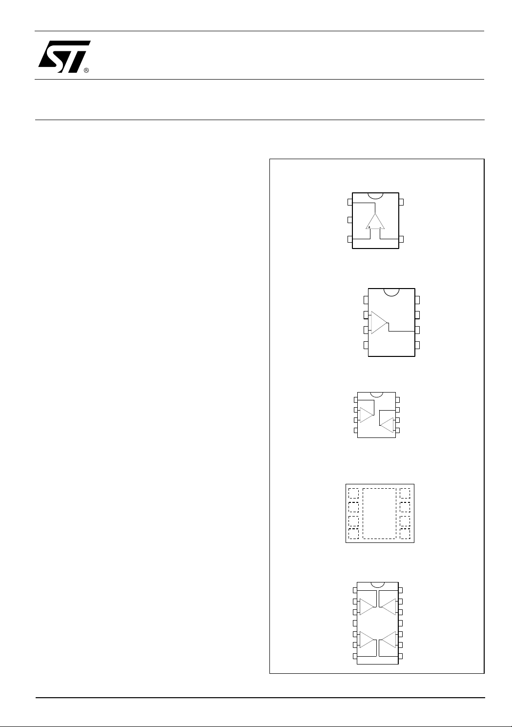
Pin Connections (top view)
TS971ILT
Output
1
V
2
DD
Non-inverting input
3
TS971ID-TS971IDT
1
N.C.
Inverting Input 1
Non-inverting Input 1
2
-
+
3
V
4
DD
TS972IN-TS972ID-TS972IDT-TS972IPT
Inverting Input 1
Non-inverting Input 1
-
2
+
3
V
45
DD
1
Output 1
TS972IQT: QFN8
Output 1
Output 1
1
1
2
Inverting Input 1
Inverting Input 1
Non Inverting Input 1
Non Inverting Input 1
2
3
3
45
45
VDD
VDD
5
4
8
7
-
6
+
8
8
7
7
6
6
V
CC
Inverting input
N.C.
8
V
7
CC
6
Output 2
N.C.
5
V
CC
Output 2
Inverting Input 2
Non-inverting Input 2
VCC
VCC
Output 2
Output 2
Inverting Input 2
Inverting Input 2
Non Inverting Input 2
Non Inverting Input 2
TS974IN-TS974ID-TS974IDT-TS974IPT
Output 4
Output 1
Inverting Input 1
Non-inverting Input 1
V
Non-inverting Input 2
Inverting Input 2
Output 2
1
2
-
+
3
4
CC
5
+
-
6
7
14
13
-
+
12
11
10
+
9
8
Inverting Input 4
Non-inverting Input 4
V
DD
Non-inverting Input 3
Inverting Input 3
Output 3
May 2005 Revision 2 1/15
TS971-TS972-TS974
Order Codes
Part Number Temperature Range Package Packaging Marking
TS971ID/IDT
TS971ILT SOT23-5L Tape & Reel K120
TS972IN DIP Tube
TS972ID/IDT SO Tube or Tape & Reel
TS972IPT
-40°C, +125°C
TS972IQT
TS974IN DIP Tube
TS974ID/IDT SO Tube or Tape & Reel
TS974IPT
(Thin Shrink Outline Package)
(dual micro lead frame package)
(Thin Shrink Outline Package)
SO Tube or Tape & Reel
TSSOP
QFN
TSSOP
Tape & Reel
Tape & Reel
Tape & Reel
2/15
TS971-TS972-TS974 Absolute Maximum Ratings
1 Absolute Maximum Ratings
Table 1: Key parameters and their absolute maximum ratings
Symbol Parameter Value Unit
V
T
T
Supply voltage
CC
V
Differential Input Voltage
id
V
Input Voltage
in
Operating Free Air Temperature Range
oper
Storage Temperature Range
stg
T
Maximum Junction Temperature
j
Thermal Resistance Junction to Ambient 4
SOT23-5
thja
QFN8
SO8
R
SO14
TSSOP8
TSSOP14
HBM: Human Body Model
ESD
MM: Machine Model
CDM: Charged Device Model 1.5 kV
Lead Temperature (soldering, 10sec) 260 °C
1) All voltage values, except differential voltage are with respect to network ground terminal.
2) Differential voltages are the non-inverting input terminal with respect to the inverting input terminal.
3) The magnitude of input and output voltages must never exceed VCC +0.3V.
4) Short-circuits can cause excessive heating and destructive dissipation.
5) Human body model, 100pF discharged through a 1.5kΩ resistor into pin of device.
6) Machine model ESD, a 200pF cap is charged to the specified voltage, then discharged directly into the IC with no external series resistor
(internal resistor < 5
1
2
3
5
6
Ω), into pin to pin of device.
12 V
±VCC V
Vdd-0.3 to Vcc+0.3 V
-40 to +125 °C
-65 to +150
150 °C
250
°C/W
50
125
103
120
100
2kV
200 V
Table 2: Operating Conditions
Symbol Parameter Value Unit
V
V
Topper Operating Free Air Temperature Range -40 to +125 °C
3/15
Supply voltage
CC
Common Mode Input Voltage Range
icm
2.7 to 10 V
+1.15 to VCC -1.15
V
DD
V
TS971-TS972-TS974 Electrical Characteristics
2 Electrical Characteristics
Table 3: V
= +2.5V, V
CC
Symbol Parameter Min. Typ. Max. Unit
Input Offset Voltage
V
io
T
≤ T
≤ T
amb
= 0V, Vo = 0V
= 0V, Vo = 0V
DV
min
Input Offset Voltage Drift
io
V
icm
Input Offset Current
I
io
V
icm
Input Bias Current
I
V
ib
V
icm
CMR
SVR
A
vd
V
OH
V
OL
I
source
I
sink
I
cc
GBP
SR
∅m
Gm
e
THD
n
= 0V, Vo = 0V
icm
≤ T
T
min
amb
≤ T
Common Mode Input Voltage Range
Common Mode Rejection Ratio
V
= ±1.35V
icm
Supply Voltage Rejection Ratio
Vcc = ±2V to ±3V 60 70
Large Signal Voltage Gain RL = 2kΩ
High Level Output Voltage RL = 2kΩ
Low Level Output Voltage RL = 2kΩ
Output Source Current
Output Sink Current
Supply Current - per amplifier
Unity gain - No load 2 2.8
Gain Bandwidth Product
f = 100kHz R
Slew Rate
= 1, Vin = ±1V
A
V
Phase Margin at Unit Gain R
Gain Margin R
Equivalent Input Noise Voltage
f = 100kHz 4
Total Harmonic Distortion
f = 1KHz
, A
v
= -2.5V, T
DD
max
max
= 25°C (unless otherwise specified)
amb
= 2kΩ, CL = 100pF
L
= 2kΩ, CL =100pF
L
= 2kΩ, CL =100pF
L
= -1 RL =10kΩ
157mV
µV/°C
5
nA
10 150
nA
200
200
750
1000
-1.35 1.35 V
dB
60 85
dB
70 80 dB
22.4 V
-2.4 -2 V
1.5 mA
100 mA
mA
MHz
8.5 12
V/
µs
2.8 4
60 Degrees
10 dB
nV
-----------Hz
%
0.003
4/15
TS971-TS972-TS974 Electrical Characteristics
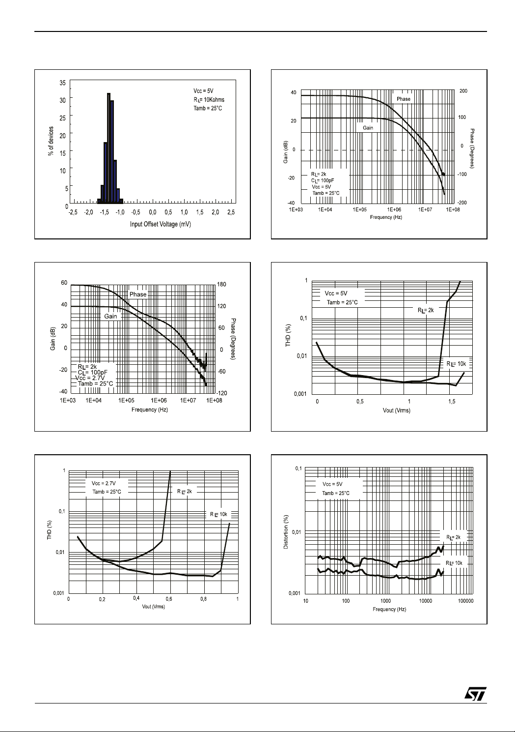
Figure 1: Input offset voltage distribution
Figure 2: Voltage gain & phase vs. frequency
Figure 4: Voltage gain & phase vs. frequency
Figure 5: THD vs. Vout
Figure 3: THD vs. Vout
5/15
Figure 6: THD vs. frequency

TS971-TS972-TS974 Electrical Characteristics
Figure 7: Noise voltage vs. frequency
Figure 8: Phase margin vs. Iout
Figure 10: Gain bandwidth product vs. Iout
Figure 11: Phase margin vs. Vcc
Figure 9: Phase margin vs. Vcc
6/15
Figure 12: Gain margin vs. Vcc

TS971-TS972-TS974 Package Mechanical Data
3 Package Mechanical Data
3.1 DIP8 package
Plastic DIP-8 MECHANICAL DATA
DIM.
A 3.3 0.130
a1 0.7 0.028
B 1.39 1.65 0.055 0.065
B1 0.91 1.04 0.036 0.041
b 0.5 0.020
b1 0.38 0.5 0.015 0.020
D 9.8 0.386
E 8.8 0.346
e 2.54 0.100
e3 7.62 0.300
e4 7.62 0.300
F 7.1 0.280
I 4.8 0.189
L 3.3 0.130
Z 0.44 1.6 0.017 0.063
MIN. TYP MAX. MIN. TYP. MAX.
mm. inch
7/15
P001F

TS971-TS972-TS974 Package Mechanical Data
3.2 SO8 package
SO-8 MECHANICAL DATA
DIM.
A 1.35 1.75 0.053 0.069
A1 0.10 0.25 0.04 0.010
A2 1.10 1.65 0.043 0.065
B 0.33 0.51 0.013 0.020
C 0.19 0.25 0.007 0.010
D 4.80 5.00 0.189 0.197
E 3.80 4.00 0.150 0.157
e 1.27 0.050
H 5.80 6.20 0.228 0.244
h 0.25 0.50 0.010 0.020
L 0.40 1.27 0.016 0.050
k ˚ (max.)
ddd 0.1 0.04
MIN. TYP MAX. MIN. TYP. MAX.
mm. inch
8
8/15
0016023/C

Package Mechanical Data TS971-TS972-TS974
3.3 TSSOP8 package
TSSOP8 MECHANICAL DATA
DIM.
A 1.2 0.047
A1 0.05 0.15 0.002 0.006
A2 0.80 1.00 1.05 0.031 0.039 0.041
b 0.19 0.30 0.007 0.012
c 0.09 0.20 0.004 0.008
D 2 .90 3.00 3.10 0.114 0.118 0.12 2
E 6.20 6.40 6.60 0.244 0.252 0.260
E1 4.30 4.40 4.50 0.169 0.173 0.177
e 0.65 0.0256
K0˚ 8˚0˚ 8˚
L 0.45 0.60 0.75 0.018 0.024 0.030
L1 1 0 .039
MIN. TYP MAX. MIN. TYP. MAX.
mm. inch
0079397/D
9/15

TS971-TS972-TS974 Package Mechanical Data
3.4 DIP14 package
Plastic DIP-14 MECHANICAL DATA
DIM.
a1 0.51 0.020
B 1.39 1.65 0.055 0.065
b 0.5 0.020
b1 0.25 0.010
D 20 0.787
E 8.5 0.335
e 2.54 0.100
e3 15.24 0.600
F 7.1 0.280
I 5.1 0.201
L 3.3 0.130
Z 1.27 2.54 0.050 0.100
MIN. TYP MAX. MIN. TYP. MAX.
mm. inch
10/15
P001A

Package Mechanical Data TS971-TS972-TS974
3.5 SO14 package
SO-14 MECHANICAL DATA
DIM.
A 1.75 0.068
a1 0.1 0.2 0.003 0.007
a2 1.65 0.064
b 0.35 0.46 0.013 0.018
b1 0.19 0.25 0.007 0.010
C 0.5 0.019
c1 45˚ (typ.)
D 8.55 8.75 0.336 0.344
E 5.8 6.2 0.228 0.244
e 1.27 0.050
e3 7.62 0.300
F 3.8 4.0 0.149 0.157
G 4.6 5. 3 0.181 0.208
L 0.5 1.27 0.019 0.050
M 0.68 0.026
S˚ (max.)
MIN. TYP MAX. MIN. TYP. MAX.
mm. inch
8
PO13G
11/15

TS971-TS972-TS974 Package Mechanical Data
3.6 TSSOP14 package
TSSOP14 MECHANICAL DATA
DIM.
A 1.2 0.047
A1 0.05 0.15 0.002 0.004 0.006
A2 0.8 1 1.05 0.031 0.039 0.041
b 0.19 0.30 0.007 0.012
c 0.09 0.20 0.004 0.0089
D 4.9 5 5.1 0.193 0.197 0.201
E 6.2 6.4 6.6 0.244 0.252 0.260
E1 4.3 4.4 4.48 0.169 0.173 0.176
e 0.65 BSC 0.0256 BSC
K0˚ 8˚0˚ 8˚
L 0.45 0.60 0.75 0.018 0.024 0.030
A
MIN. TYP MAX. MIN. TYP. MAX.
A2
b
A1
mm. inch
e
D
c
K
L
E
12/15
PIN 1 IDENTIFICATION
E1
1
0080337D

Package Mechanical Data TS971-TS972-TS974
3.7 SOT23-5 package
SOT23-5L MECHANICAL DATA
DIM.
A 0.90 1.45 35.4 57.1
A1 0.00 0.15 0.0 5.9
A2 0.90 1.30 35.4 51.2
b 0.35 0.50 13.7 19.7
C 0.09 0.20 3.5 7.8
D 2.80 3.00 110.2 118.1
E 2.60 3.00 102.3 118.1
E1 1.50 1.75 59.0 68.8
e.95 37.4
e1 1.9 74.8
L 0.35 0.55 13.7 21.6
MIN. TYP MAX. MIN. TYP. MAX.
mm. mils
0
13/15

TS971-TS972-TS974 Package Mechanical Data
3.8 DFN8 package
14/15

Revision History TS971-TS972-TS974
4 Revision History
Date Revision Description of Changes
Nov. 2002 1 First Release
May 2005 3 Modifications on AMR Table 1 on page 3 (explanation of Vid and Vi limits)
Information furnished is believed to be accurate and reliable. However, STMicroelectronics assumes no responsibility for the consequences
of use of such information nor for any infringement of patents or other rights of third parties which may result from its use. No license is granted
by implication or otherwise under any patent or patent rights of STMicroelectronics. Specifications mentioned in this publication are subject
to change without notice. This publication supersedes and replaces all information previously supplied. STMicroelectronics products are not
authorized for use as critical components in life support devices or systems without express written approval of STMicroelectronics.
The ST logo is a registered trademark of STMicroelectronics
All other names are the property of their respective owners
© 2005 STMicroelectronics - All rights reserved
Australia - Belgium - Brazil - Canada - China - Czech Republic - Finland - France - Germany - Hong Kong - India - Israel - Italy - Japan -
Malaysia - Malta - Morocco - Singapore - Spain - Sweden - Switzerland - United Kingdom - United States of America
STMicroelectronics group of companies
www.st.com
15/15
 Loading...