

STMicroelectronics TS931, TS932, TS934 Technical data
Output Rail-to-Rail Micropow er Operational Amplifiers
n
Rail-to-rail output voltage swing
n
Microp ower consum p t io n (2 0µA)
n
Single supply operation (2.7V to 10V
n
Low offset (2mV max for TS93xB)
n
CMOS inputs
n
Ultra low input bias current (1pA)
n
ESD protecti on (2kV)
n
Latch-up immunity (class A)
n
Available in SOT23-5 micropackage
Description
The TS93x (single, dual & quad) series are
operational amplifiers able to operate with voltage
as low as 2.7V and to reach 2.9Vpp of output
swing with R
Offering a typical consumption of only 20
are particularly well-suited for battery-powered
applications.
Fitting the TS93x o nto your board design is very
easy because of its space-saving 5-pin SOT23-5
package with outer dimensions of
2.8mm x 2.9mm.
Applications
n
Battery-powered systems
n
Portable communication systems
n
Alarm, smoke detectors
n
Instrumentation & sensoring
n
PH Meter
n
Digi t a l s c ales
= 100kΩ when supplied @ 3V.
L
µA, they
TS931-TS932-TS934
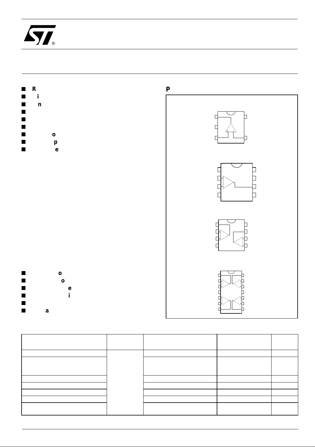
Pin Connections (top view)
TS931ILT
Output
1
V
2
DD
Non-inverting input
3
TS931ID-TS931IDT
1
N.C.
Inverting Input 1
Non-inverting Input 1
2
-
+
3
V
4
DD
TS932IN-TS932ID-TS932IDT
1
Output 1
Inverting Input 1
Non-inverting Input 1
V
-
2
+
3
45
DD
TS934IN-TS934ID-TS934IDT-TS934IPT
Output 1
Output 2
V
1
2
-
+
3
4
CC
5
+
-
6
7
Inverting Input 1
Non-inverting Input 1
Non-inverting Input 2
Inverting Input 2
5
4
8
7
-
6
+
14
13
-
+
12
11
10
+
-
9
8
V
CC
Inverting input
V
CC
Output 2
Inverting Input 2
Non-inverting Input 2
Output 4
Inverting Input 4
Non-inverting Input 4
V
DD
Non-inverting Input 3
Inverting Input 3
Output 3
N.C.
8
V
7
6
Output 2
N.C.
5
CC
Order Codes
Part Number
TS931ID/IDT/AID/AIDT/BID/BIDT
TS931ILT/AILT/BILT SOT23-5L Tape & Reel
TS932IN/AIN/BIN DIP Tube
TS932ID/IDT/AID/AIDT/BID/BIDT SO Tube or Tape & Reel
TS934IN/AIN/BIN DIP Tube
TS934ID/IDT/AID/AIDT/BIDT/BIDT SO Tube or Tape & Reel
TS934IPT/AIPT/BIPT
December 2004 Revision 2 1/15
Temperature
Range
-40°C, +85°C
Package Packaging Marking
SO Tube or Tape & Reel
TSSOP
(Thin Shrink Outline Package)
K205
K206
K207
Tape & Reel

TS931-TS932-TS934 Absolute Maximum Ratings
1 Absolute Maximum Ratings
Table 1: Key parameter s and their abs olute maxi mum ratin gs
Symbol Parameter Value Unit
VCC
T
T
R
Supply voltage
Vid
Differential Input Voltage
V
Input Voltage Range
in
Operating Free Air Temperature Range
oper
Storage Temperature Range
std
T
Maximum Junction Temperature
j
Thermal Resistance Junction to Ambient
thja
SOT23-5
DIP8
DIP14
SO8
SO14
TSSOP8
TSSOP14
HBM: Human Body Model
ESD
MM: Machine Model
CDM: Charged Device Model 2 kV
Latch-up Immunity 200 mA
Soldering Temperature (10sec), leaded version 250 °C
1) All v ol tages val u es, except dif ferent i a l vol t age are with respect to net w ork term i n al.
2) Dif ferential vol t ages are non-inverti ng input termi nal with respect to th e i nverting in put terminal .
3) The magnitude of input and out put voltage s m ust never exc eed VCC +0.3V.
4) Short-circuits can cause excessive heating and destructive dissipation.
5) Human body model, 100pF discharged thr ough a 1.5kΩ resistor into pin of device.
6) Machine model ESD, a 200pF cap is charged to the specified voltage, then discharged directly into the IC with no external series resistor
(inter nal resistor < 5
1
2
3
5
6
Ω), into pin to pin of device.
12 V
±12 V
Vdd-0.3 to Vcc+0.3 V
-40 to + 85 °C
-65 to +150 °C
150 °C
4
°C/W
250
85
66
125
103
120
100
2kV
200 V
Table 2: Operating Conditions
Symbol Parameter Value Unit
VCC Supply Voltage 2.7 to 10 V
2/15
Vicm
T
oper
Common Mode Input Voltage Range V
Operating Free Air Temperature Range
- 0.2 to VCC - 1.5
dd
-40 to + 85 °C
V

Electrical Characteristics TS931-TS932-TS934
2 Electrical Characteristics
Tables 3 and 4 give the electrical characteristics at each Vcc value.
Table 3: V
= +3V, Vdd = 0V, T
CC
= 25°C (unless otherwise specified)
amb
Symbol Parameter Min. Typ. Max. Unit
Input Offset Voltage
V
io
∆V
I
io
I
ib
CMR
SVR
Input Offset Voltage Drift
io
Input Offset Current
Input Bias Current
1)
Common Mode Rejection Ratio
0
≤ V
≤ VCC - 1.7
icm
Supply Voltage Rejection Ratio
TS931/2/4
TS931/2/4A
TS931/2/4B
3
1
1 100 pA
1 150 pA
85 dB
2
85 dB
10
5
2
µV/°C
Large Signal Voltage Gain
V
A
vd
V
OH
V
OL
= 2Vpp RL = 1MΩ
O
RL = 100kΩ
High Level Output Voltage
V
= 100mV RL = 100kΩ
ID
Low Level Output Voltage
V
= -100mV RL = 100kΩ
ID
120
106
2.95
50
Output Source Current
V
I
o
I
CC
GBP
SR
φm
= 100mV, VO = V
ID
DD
Output Sink Current
V
= -100mV, VO = V
ID
CC
Supply Current (per amplifier)
= 1, no load
A
VCL
Gain Bandwidth Product R
Slew Rate R
Phase Margin C
= 100kΩ, CL = 50pF
L
= 100kΩ, CL = 50pF
L
= 50pF
L
1.5
1.5
20 31
100 kHz
50 V/ms
65 Degrees
en Input Voltage Noise 75 nV/
mV
dB
V
mV
mA
µA
√Hz
1) Maximum values including unavoidable inaccurates of the industrial test.
2) VCC has a 0.2V vari ation.
3/15

TS931-TS932-TS934 Electrical Characteristics
Table 4: V
= +5V, Vdd = 0V, T
CC
= 25°C (unless otherwise specified)
amb
Symbol Parameter Min. Typ. Max. Unit
Input Offset Voltage
V
io
∆V
I
io
I
ib
CMR
SVR
TS931/2/4
TS931/2/4A
TS931/2/4B
Input Offset Voltage Drift 3 µV/°C
io
Input Offset Current
Input Bias Current
1
1)
Common Mode Rejection Ratio
0
≤ V
≤ VCC - 1.7
icm
Supply Voltage Rejection Ratio
2
1 100 pA
1 150 pA
85 dB
85 dB
10
5
2
Large Signal Voltage Gain
A
O
vd
RL = 100kΩ
V
V
High Level Output Voltage
OH
V
= 100mV RL = 100kΩ
ID
Low Level Output Voltage
OL
V
= -100mV RL = 100kΩ
ID
4.95
120
112
50
= 4Vpp RL = 1MΩ
V
Output Source Current
V
I
o
I
CC
GBP
SR
φm
= 100mV, VO = V
ID
DD
Output Sink Current
V
= -100mV, VO = V
ID
CC
Supply Current (per amplifier)
= 1, no load
A
VCL
Gain Bandwidth Product R
Slew Rate R
Phase Margin C
= 100KΩ, CL = 50pF
L
= 100KΩ, CL = 50pF
L
= 50pF
L
5
5
20 33
100 kHz
50 V/ms
65 Degrees
en Input Voltage Noise 76 nV/
mV
dB
V
mV
mA
µA
√Hz
1) Maximum values including unavoidable inaccurates of the industrial test.
2) V
has a 0.2V vari ation.
CC
4/15

Electrical Characteristics TS931-TS932-TS934
Figure 1:
50
0
-50
Input Offset Voltage Drift ( V)µ
-100
-150
-40 -20 0 20 40 60 80
Figure 2:
12
10
8
Vcc=5V
Temperature (°C)
Vid=-100mV
Vid=+100mV
Figure 4:
20
18
16
14
12
10
8
6
Supply Current ( A)µ
4
2
0
024681012
SupplyVoltage (V)
Tamb=25°CTamb=25°C
Figure 5:
21
Vcc from 2.7V to 10V
20
19
6
4
Supply Current ( A)µ
2
0
024681012
SupplyVoltage (V)
Figure 3:
6
4
2
0
-2
-4
Output Short-Circuit Current (mA)
-6
-40 -20 0 20 40 60 80
Temperature (°C)
Isink,Vcc=5V
Isink,Vcc=3V
Isource,Vcc=3V
Isource,Vcc=5V
Tamb=25°CTamb=25°C
18
Supply Current ( A)µ
17
16
-40 -20 0 20 40 60 80
Figure 6:
30
20
10
0
-10
-20
Output Short-Circuit Current (mA)
-30
246810
Temperature (°C)
Tamb=25°C
Sink
Source
SupplyVoltage (V)
5/15
 Loading...