

Page 1
Output Rail-to-Rail Micropow er Operational Amplifiers
n
Rail-to-rail output voltage swing
n
Microp ower consum p t io n (2 0µA)
n
Single supply operation (2.7V to 10V
n
Low offset (2mV max for TS93xB)
n
CMOS inputs
n
Ultra low input bias current (1pA)
n
ESD protecti on (2kV)
n
Latch-up immunity (class A)
n
Available in SOT23-5 micropackage
Description
The TS93x (single, dual & quad) series are
operational amplifiers able to operate with voltage
as low as 2.7V and to reach 2.9Vpp of output
swing with R
Offering a typical consumption of only 20
are particularly well-suited for battery-powered
applications.
Fitting the TS93x o nto your board design is very
easy because of its space-saving 5-pin SOT23-5
package with outer dimensions of
2.8mm x 2.9mm.
Applications
n
Battery-powered systems
n
Portable communication systems
n
Alarm, smoke detectors
n
Instrumentation & sensoring
n
PH Meter
n
Digi t a l s c ales
= 100kΩ when supplied @ 3V.
L
µA, they
TS931-TS932-TS934
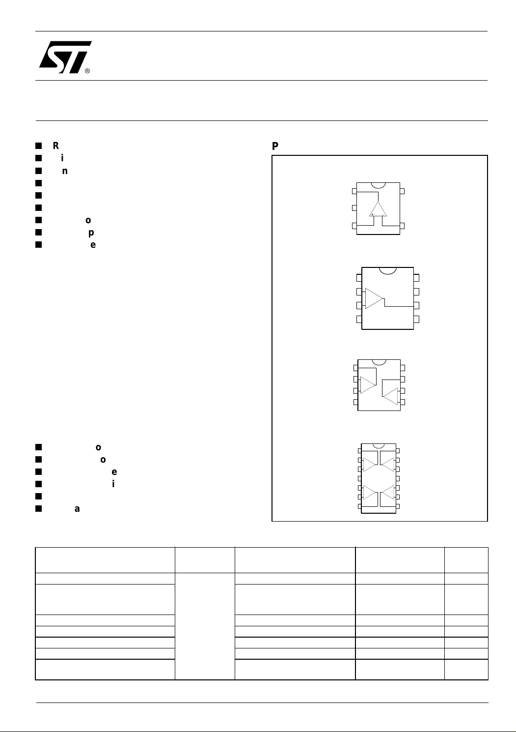
Pin Connections (top view)
TS931ILT
Output
1
V
2
DD
Non-inverting input
3
TS931ID-TS931IDT
1
N.C.
Inverting Input 1
Non-inverting Input 1
2
-
+
3
V
4
DD
TS932IN-TS932ID-TS932IDT
1
Output 1
Inverting Input 1
Non-inverting Input 1
V
-
2
+
3
45
DD
TS934IN-TS934ID-TS934IDT-TS934IPT
Output 1
Output 2
V
1
2
-
+
3
4
CC
5
+
-
6
7
Inverting Input 1
Non-inverting Input 1
Non-inverting Input 2
Inverting Input 2
5
4
8
7
-
6
+
14
13
-
+
12
11
10
+
-
9
8
V
CC
Inverting input
V
CC
Output 2
Inverting Input 2
Non-inverting Input 2
Output 4
Inverting Input 4
Non-inverting Input 4
V
DD
Non-inverting Input 3
Inverting Input 3
Output 3
N.C.
8
V
7
6
Output 2
N.C.
5
CC
Order Codes
Part Number
TS931ID/IDT/AID/AIDT/BID/BIDT
TS931ILT/AILT/BILT SOT23-5L Tape & Reel
TS932IN/AIN/BIN DIP Tube
TS932ID/IDT/AID/AIDT/BID/BIDT SO Tube or Tape & Reel
TS934IN/AIN/BIN DIP Tube
TS934ID/IDT/AID/AIDT/BIDT/BIDT SO Tube or Tape & Reel
TS934IPT/AIPT/BIPT
December 2004 Revision 2 1/15
Temperature
Range
-40°C, +85°C
Package Packaging Marking
SO Tube or Tape & Reel
TSSOP
(Thin Shrink Outline Package)
K205
K206
K207
Tape & Reel
Page 2

TS931-TS932-TS934 Absolute Maximum Ratings
1 Absolute Maximum Ratings
Table 1: Key parameter s and their abs olute maxi mum ratin gs
Symbol Parameter Value Unit
VCC
T
T
R
Supply voltage
Vid
Differential Input Voltage
V
Input Voltage Range
in
Operating Free Air Temperature Range
oper
Storage Temperature Range
std
T
Maximum Junction Temperature
j
Thermal Resistance Junction to Ambient
thja
SOT23-5
DIP8
DIP14
SO8
SO14
TSSOP8
TSSOP14
HBM: Human Body Model
ESD
MM: Machine Model
CDM: Charged Device Model 2 kV
Latch-up Immunity 200 mA
Soldering Temperature (10sec), leaded version 250 °C
1) All v ol tages val u es, except dif ferent i a l vol t age are with respect to net w ork term i n al.
2) Dif ferential vol t ages are non-inverti ng input termi nal with respect to th e i nverting in put terminal .
3) The magnitude of input and out put voltage s m ust never exc eed VCC +0.3V.
4) Short-circuits can cause excessive heating and destructive dissipation.
5) Human body model, 100pF discharged thr ough a 1.5kΩ resistor into pin of device.
6) Machine model ESD, a 200pF cap is charged to the specified voltage, then discharged directly into the IC with no external series resistor
(inter nal resistor < 5
1
2
3
5
6
Ω), into pin to pin of device.
12 V
±12 V
Vdd-0.3 to Vcc+0.3 V
-40 to + 85 °C
-65 to +150 °C
150 °C
4
°C/W
250
85
66
125
103
120
100
2kV
200 V
Table 2: Operating Conditions
Symbol Parameter Value Unit
VCC Supply Voltage 2.7 to 10 V
2/15
Vicm
T
oper
Common Mode Input Voltage Range V
Operating Free Air Temperature Range
- 0.2 to VCC - 1.5
dd
-40 to + 85 °C
V
Page 3

Electrical Characteristics TS931-TS932-TS934
2 Electrical Characteristics
Tables 3 and 4 give the electrical characteristics at each Vcc value.
Table 3: V
= +3V, Vdd = 0V, T
CC
= 25°C (unless otherwise specified)
amb
Symbol Parameter Min. Typ. Max. Unit
Input Offset Voltage
V
io
∆V
I
io
I
ib
CMR
SVR
Input Offset Voltage Drift
io
Input Offset Current
Input Bias Current
1)
Common Mode Rejection Ratio
0
≤ V
≤ VCC - 1.7
icm
Supply Voltage Rejection Ratio
TS931/2/4
TS931/2/4A
TS931/2/4B
3
1
1 100 pA
1 150 pA
85 dB
2
85 dB
10
5
2
µV/°C
Large Signal Voltage Gain
V
A
vd
V
OH
V
OL
= 2Vpp RL = 1MΩ
O
RL = 100kΩ
High Level Output Voltage
V
= 100mV RL = 100kΩ
ID
Low Level Output Voltage
V
= -100mV RL = 100kΩ
ID
120
106
2.95
50
Output Source Current
V
I
o
I
CC
GBP
SR
φm
= 100mV, VO = V
ID
DD
Output Sink Current
V
= -100mV, VO = V
ID
CC
Supply Current (per amplifier)
= 1, no load
A
VCL
Gain Bandwidth Product R
Slew Rate R
Phase Margin C
= 100kΩ, CL = 50pF
L
= 100kΩ, CL = 50pF
L
= 50pF
L
1.5
1.5
20 31
100 kHz
50 V/ms
65 Degrees
en Input Voltage Noise 75 nV/
mV
dB
V
mV
mA
µA
√Hz
1) Maximum values including unavoidable inaccurates of the industrial test.
2) VCC has a 0.2V vari ation.
3/15
Page 4

TS931-TS932-TS934 Electrical Characteristics
Table 4: V
= +5V, Vdd = 0V, T
CC
= 25°C (unless otherwise specified)
amb
Symbol Parameter Min. Typ. Max. Unit
Input Offset Voltage
V
io
∆V
I
io
I
ib
CMR
SVR
TS931/2/4
TS931/2/4A
TS931/2/4B
Input Offset Voltage Drift 3 µV/°C
io
Input Offset Current
Input Bias Current
1
1)
Common Mode Rejection Ratio
0
≤ V
≤ VCC - 1.7
icm
Supply Voltage Rejection Ratio
2
1 100 pA
1 150 pA
85 dB
85 dB
10
5
2
Large Signal Voltage Gain
A
O
vd
RL = 100kΩ
V
V
High Level Output Voltage
OH
V
= 100mV RL = 100kΩ
ID
Low Level Output Voltage
OL
V
= -100mV RL = 100kΩ
ID
4.95
120
112
50
= 4Vpp RL = 1MΩ
V
Output Source Current
V
I
o
I
CC
GBP
SR
φm
= 100mV, VO = V
ID
DD
Output Sink Current
V
= -100mV, VO = V
ID
CC
Supply Current (per amplifier)
= 1, no load
A
VCL
Gain Bandwidth Product R
Slew Rate R
Phase Margin C
= 100KΩ, CL = 50pF
L
= 100KΩ, CL = 50pF
L
= 50pF
L
5
5
20 33
100 kHz
50 V/ms
65 Degrees
en Input Voltage Noise 76 nV/
mV
dB
V
mV
mA
µA
√Hz
1) Maximum values including unavoidable inaccurates of the industrial test.
2) V
has a 0.2V vari ation.
CC
4/15
Page 5

Electrical Characteristics TS931-TS932-TS934
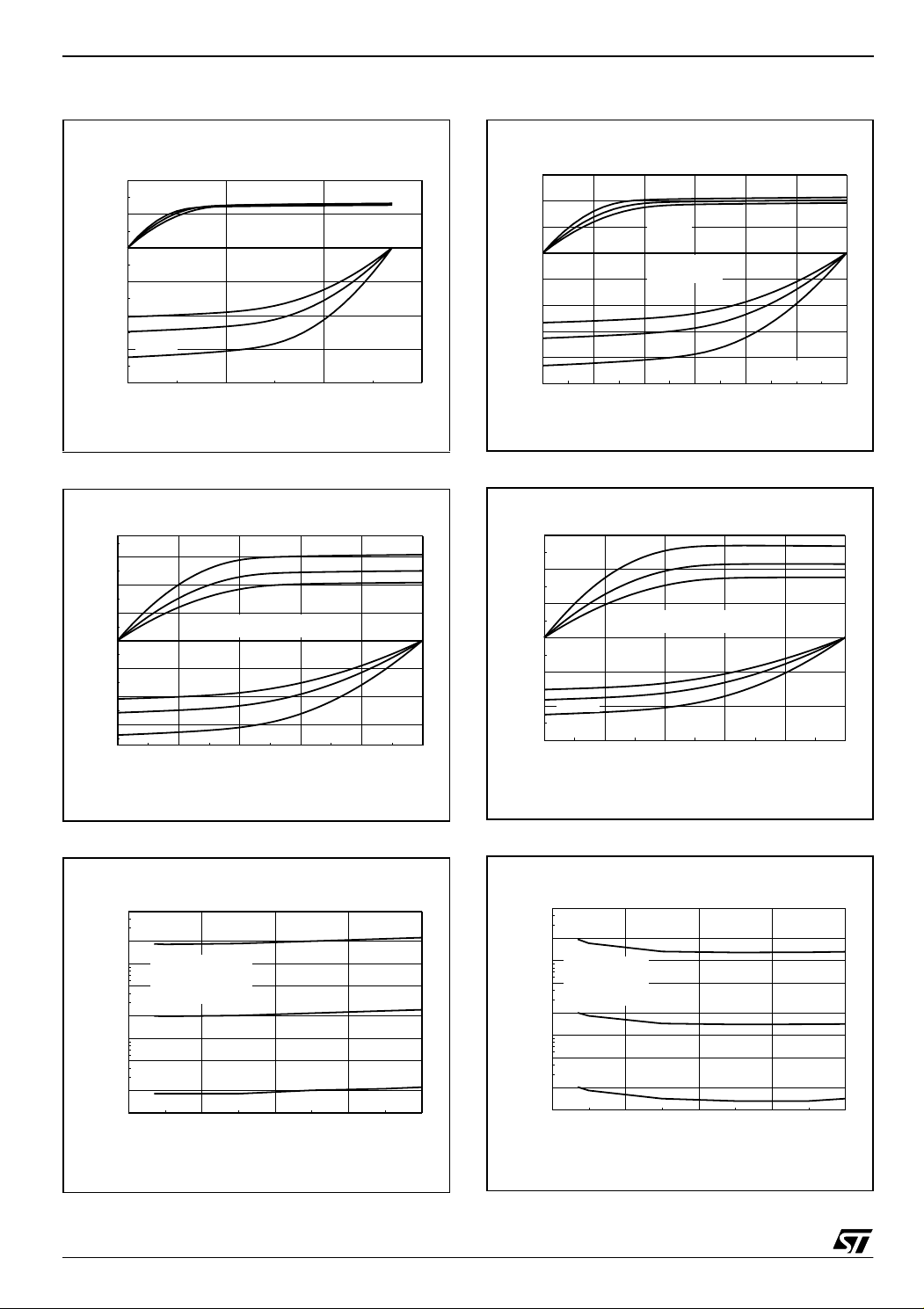
Figure 1:
50
0
-50
Input Offset Voltage Drift ( V)µ
-100
-150
-40 -20 0 20 40 60 80
Figure 2:
12
10
8
Vcc=5V
Temperature (°C)
Vid=-100mV
Vid=+100mV
Figure 4:
20
18
16
14
12
10
8
6
Supply Current ( A)µ
4
2
0
024681012
SupplyVoltage (V)
Tamb=25°CTamb=25°C
Figure 5:
21
Vcc from 2.7V to 10V
20
19
6
4
Supply Current ( A)µ
2
0
024681012
SupplyVoltage (V)
Figure 3:
6
4
2
0
-2
-4
Output Short-Circuit Current (mA)
-6
-40 -20 0 20 40 60 80
Temperature (°C)
Isink,Vcc=5V
Isink,Vcc=3V
Isource,Vcc=3V
Isource,Vcc=5V
Tamb=25°CTamb=25°C
18
Supply Current ( A)µ
17
16
-40 -20 0 20 40 60 80
Figure 6:
30
20
10
0
-10
-20
Output Short-Circuit Current (mA)
-30
246810
Temperature (°C)
Tamb=25°C
Sink
Source
SupplyVoltage (V)
5/15
Page 6
TS931-TS932-TS934 Electrical Characteristics
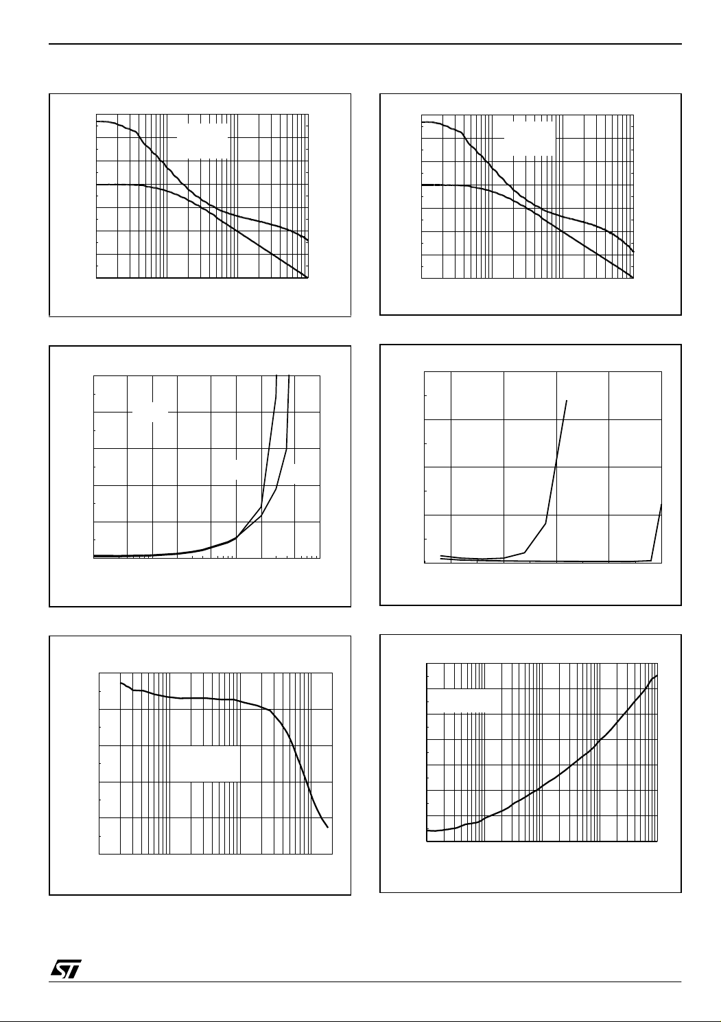
Figure 7:
1
0.5
0
-0.5
-1
-1.5
Output Short-Circuit Current (mA)
-2
0123
Sink
T=+85°C
T=+25°C
T=-40°C
T=-40°C
T=+25°C
T=+85°C
Vcc=2.7V
Source
OutputVoltage (V)
Figure 8:
6
Sink
4
2
0
-2
-4
Output Short-Circuit Current (mA)
-6
012345
T=+85°C
Vcc=5V
T=+25°C
T=-40°C
OutputVoltage (V)
T=-40°C
T=+25°C
T=+85°C
Source
Figure 10:
Sink
1
0
T=-40°C
T=+25°C
T=+85°C
Vcc=3V
-1
T=+85°C
T=+25°C
Output Short-Circuit Current (mA)
-2
T=-40°C
0 0.5 1 1.5 2 2.5 3
OutputVoltage (V)
Figure 1 1:
30
Sink
20
10
Vcc=10V
0
-10
T=+85°C
-20
T=+25°C
Output Short-Circuit Current (mA)
T=-40°C
-30
0246810
OutputVoltage (V)
Source
T=-40°C
T=+25°C
T=+85°C
Source
Figure 9:
500
200
100
50
20
10
5
Voltage referenced toVcc (mV)
2
1
246810
6/15
RL tied toVDD
SINGLE SUPPLY
Vid = +100mV
RL = 10k
RL = 100k
RL = 1M
SupplyVoltage (V)
Figure 12:
500
Ω
Ω
Ω
200
100
RL tied toVcc
SINGLE SUPPLY
50
Vid = -100mV
20
10
5
Voltage referenced toVDD (mV)
2
1
246810
RL = 10k
RL = 100k
RL = 1M
SupplyVoltage (V)
Ω
Ω
Ω
Page 7
Electrical Characteristics TS931-TS932-TS934
Figure 13:
70
60
50
40
30
Gain (dB)
20
10
0
100 200 500 1,000 2,000 5,000 10,000 20,000 50,000 100,000
RL = 100k
CL = 50 pF
Vcc = 3V & 5V
Gain
Frequency (Hz)
Figure 14:
1
0.8
0.6
0.4
Distortion (%)
0.2
RL=100k
Gain = +2
Phase
Vcc=5V
Vo=4Vpp
Vcc=3V
Vo=2Vpp
180
160
140
120
100
80
60
Figure 16:
70
60
50
Phase (°)
40
30
Gain (dB)
20
10
0
100 200 500 1,000 2,000 5,000 10,000 20,000 50,000 100,000
RL = 100k
CL = 100 pF
Vcc = 3V & 5V
Gain
Frequency (Hz)
Phase
180
160
140
120
100
80
60
40
Phase (°)
Figure 17:
2
RL=100k
Gain = +2
1.5
1
Distortion (%)
0.5
F = 100Hz
Vcc=3V
Vcc=5V
0
20 50 100 200 500 1,000 2,000 5,000 10,000
Frequency (Hz)
Figure 15:
100
80
60
40
20
Equivalent NoiseVoltage (nV/ Hz)√
0
10 30 100 300 1,000 3,000 10,000
Vcc=2.7V
Rs = 100
Tamb = 25°C
Frequency (Hz)
0
12345
OutputVoltage (Vpp)
Figure 18:
-40
-45
Vcc = 5V
Gain = +1
-50
-55
-60
-65
SupplyVoltage Rejection (dB)
-70
-75
100 300 1,000 3,000 10,000 30,000 100,000 300,000 1,000,000
Frequency (Hz)
7/15
Page 8

TS931-TS932-TS934 Electrical Characteristics
Figure 19:
Voltage (50mV/div)
0 5 10 15 20 25 30 35 40 45 50
Time ( s)µ
INPUT
0V
Vcc = 5V
Gain = +1
RL = 100k
CL = 50pF
OUTPUT
0V
Figure 20:
Voltage (1V/div)
0 100 200 300 400 500
Time ( s)µ
INPUT
0V
Vcc = 5V
Gain = +1
RL = 100k
CL = 50pF
OUTPUT
0V
8/15
Page 9
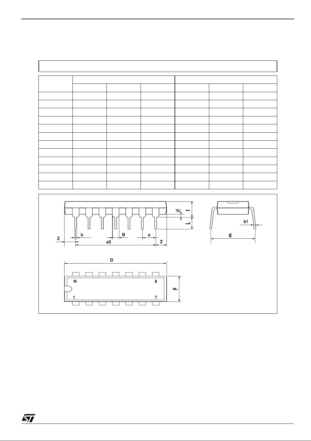
Package Mechanical Data TS931-TS932-TS934
3 Package Mechanical Data
3.1 DIP8 package
Plastic DIP-8 MECHANICAL DATA
DIM.
A 3.3 0.130
a1 0.7 0.028
B 1.39 1.65 0.055 0.065
B1 0.91 1.04 0.036 0.041
b 0.5 0.020
b1 0.38 0.5 0.015 0.020
D 9.8 0.386
E 8.8 0.346
e 2.54 0.100
e3 7.62 0.300
e4 7.62 0.300
F 7.1 0.280
I 4.8 0.189
L 3.3 0.130
Z 0.44 1.6 0.017 0.063
MIN. TYP MAX. MIN. TYP. MAX.
mm. inch
P001F
9/15
Page 10

TS931-TS932-TS934 Package Mechanical Data
3.2 SO8 package
SO-8 MECHANICAL DATA
DIM.
A 1.35 1.75 0.053 0.069
A1 0.10 0.25 0.04 0.010
A2 1.10 1.65 0.043 0.065
B 0.33 0.51 0.013 0.020
C 0.19 0.25 0.007 0.010
D 4.80 5.00 0.189 0.197
E 3.80 4.00 0.150 0.157
e 1.27 0.050
H 5.80 6.20 0.228 0.244
h 0.25 0.50 0.010 0.020
L 0.40 1.27 0.016 0.050
k ˚ (max.)
ddd 0.1 0.04
MIN. TYP MAX. MIN. TYP. MAX.
mm. inch
8
10/15
0016023/C
Page 11
Package Mechanical Data TS931-TS932-TS934
3.3 DIP14 package
Plastic DIP-14 MECHANICAL DATA
DIM.
a1 0.51 0.020
B 1.39 1.65 0.055 0.065
b 0.5 0.020
b1 0.25 0.010
D 20 0.787
E 8.5 0.335
e 2.54 0.100
e3 15.24 0.600
F 7.1 0.280
I 5.1 0.201
L 3.3 0.130
Z 1.27 2.54 0.050 0.100
MIN. TYP MAX. MIN. TYP. MAX.
mm. inch
P001A
11/15
Page 12

TS931-TS932-TS934 Package Mechanical Data
3.4 SO14 package
SO-14 MECHANICAL DATA
DIM.
A 1.75 0.068
a1 0.1 0.2 0.003 0.007
a2 1.65 0.064
b 0.35 0.46 0.013 0.018
b1 0.19 0.25 0.007 0.010
C 0.5 0.019
c1 45˚ (typ.)
D 8.55 8.75 0.336 0.344
E 5.8 6.2 0.228 0.244
e 1.27 0.050
e3 7.62 0.300
F 3.8 4.0 0.149 0.157
G 4.6 5.3 0.181 0.208
L 0.5 1.27 0.019 0.050
M 0.68 0.026
S ˚ (max.)
MIN. TYP MAX. MIN. TYP. MAX.
mm. inch
8
12/15
PO13G
Page 13

Package Mechanical Data TS931-TS932-TS934
3.5 TSSOP14 package
TSSOP14 MECHANICAL DATA
DIM.
A 1.2 0.047
A1 0.05 0.15 0.002 0.004 0.006
A2 0.8 1 1.05 0.031 0.039 0.041
b 0.19 0.30 0.007 0.012
c 0.09 0.20 0.004 0.0089
D 4.9 5 5.1 0.193 0.197 0.201
E 6.2 6.4 6.6 0.244 0.252 0.260
E1 4.3 4.4 4.48 0.169 0.173 0.176
e 0.65 BSC 0.0256 BSC
K0˚ 8˚ 0˚ 8˚
L 0.45 0.60 0.75 0.018 0.024 0.030
A
MIN. TYP MAX. MIN. TYP. MAX.
A2
b
A1
mm. inch
e
D
c
K
L
E
PIN 1 IDENTIFICATION
E1
1
0080337D
13/15
Page 14

TS931-TS932-TS934 Package Mechanical Data
3.6 SOT23-5 package
SOT23-5L MECHANICAL DATA
DIM.
A 0.90 1.45 35.4 57.1
A1 0.00 0.15 0.0 5.9
A2 0.90 1.30 35.4 51.2
b 0.35 0.50 13.7 19.7
C 0.09 0.20 3.5 7.8
D 2.80 3.00 110.2 118.1
E 2.60 3.00 102.3 118.1
E1 1.50 1.75 59.0 68.8
e.95 37.4
e1 1.9 74.8
L 0.35 0.55 13.7 21.6
MIN. TYP MAX. MIN. TYP. MAX.
mm. mils
0
14/15
Page 15
Summary of Changes TS931-TS932-TS934
4 Summary of Changes
Date Revision Description of Changes
01 Nov 2001 1 First Release
01 Dec 2004 2 Modifications on AMR table page 2 (explanation of Vid and Vi limits)
Information furnished is believed to be accurate and reliable. However, STMicroelectronics assumes no responsibility for the consequences
of use of such information nor for any infringement of patents or other rights of third parties which may result from its use. No licens e is g ran te d
by impl i cation or ot herwise under any p atent or pa tent right s of STMicroelectro ni cs. Specif i cations mentioned i n this publi cation are subject
to change without notice. This publication supersedes and replaces all information previously supplied. STMicroelectronics products are not
authori zed for use as cr i tical compon ents in life support devic es or systems without ex press written approval of STMicroel ectronics.
The ST logo is a registered trademark of STMicroelectronics
All other na m es are the prop erty of thei r res p ective ow ners
© 2004 STM i croelectr onics - All rights rese rved
Austra l i a - B el gi um - Brazil - Canada - China - Czech Republic - Finland - France - Germa ny - Hong Kong - India - Israel - Italy - Jap an -
Malaysia - M a lta - Morocco - Singapore - Spain - Sweden - Switz erland - United Kingdom - United Stat es of America
STMicroelectronic s group of comp ani es
www.st.com
15/15
 Loading...