

Page 1
TS921
Rail-to-Rail High Output Current Single Operational Amplifier
n
Rail-to -ra i l input and output
n
Low noise: 9nV/√(Hz)
n
Low distortion
n
High output current: 80mA
(able to drive 32Ω loads)
n
High-speed: 4mHz, 1V/µs
n
Operating from 2.7V to 12V
n
ESD internal protect ion: 1.5kV
n
Latch-up immunity
n
Macromodel included in this specification
Description
The TS921 is a rail-to-rail single BiCMOS
operational amplifier optimized and fully spe cified
for 3V and 5V operation.
Its high output current allows low-load
impedances to be driven.
The TS921 exhibits very low noise, low distortion
and low offset. It has a high output current
capability which makes this device an excellent
choice for high quality, low voltage or batteryoperated audio systems.
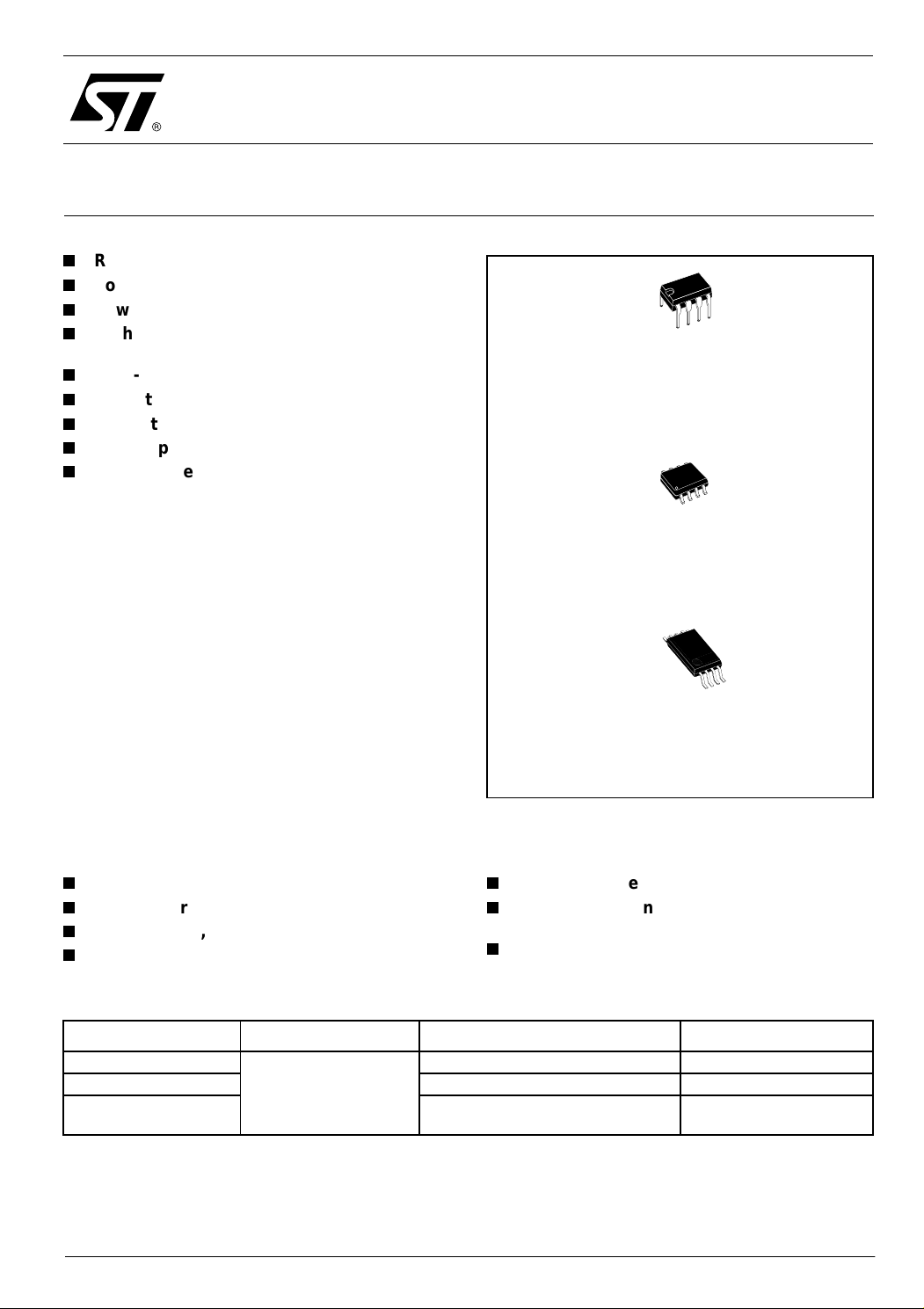
N
DIP-8
(Plastic Package)
D
SO-8
(Plastic Micropackage)
P
TSSOP8
(Thin Shrink Small Outline Package)
The device is stable for capacitive loads up to
500pF.
Applications
n
Headph on e am pl ifier
n
Piezoelectric speaker driver
n
Sound cards, multimed ia sys tem s
n
Line driver, actuator driver
n
Servo am pl ifi er
n
Mobile phone a nd po rtabl e commu nicati on
sets
n
Instrumentation with low noise as key
factor
Order Codes
Part Number Temperature Range Package Packaging
TS921IN
TS921ID/IDT SO Tube or Tape & Reel
TS921IPT
December 2004 Revision 2 1/13
-40°C, +125°C
(Thin Shrink Outline Package)
DIP Tube
TSSOP
Tape & Reel
Page 2
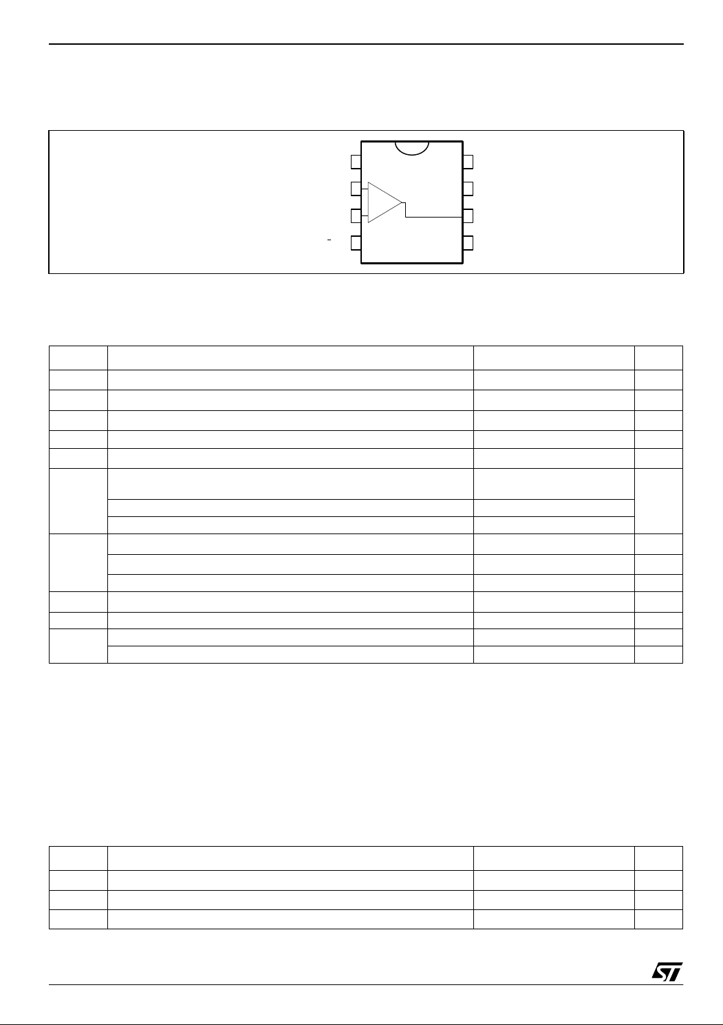
TS921 Pin Diagram
1 Pin Diagram
Figure 1 : Pin co nn e ct io ns (top view)
N.C.
Inverting Input
Non-inverting Input
V
1
2
-
+
3
45
CC
8
7
6
N.C.
V
CC
Output
N.C.
+
2 Absolute Maximum Ratings
Table 1: Key parameters and their absolute maximum rating s
Symbol Parameter Value Unit
VCC
T
Supply voltage
Vid
Differential Input Voltage
V
Input Voltage VDD-0.3 to VCC+0.3
i
Storage Temperature
stg
Maximum Junction Temperature
T
j
Thermal Resistance Junction to Ambient
R
SO8
thja
TSSOP8 120
DIP8 85
HBM: Human Body Model
ESD
MM: Machine Model
CDM: Charged Device Model 1.5 kV
Output Short Circuit Duration
Latch-up Immunity 200 mA
Soldering Temperature (10sec), leaded version 250 °C
Soldering Temperature (10sec), unleaded version 260 °C
1) All voltages values, except differential voltage are with respect to network ground terminal.
2) Differential voltages are the non-inverting input terminal with respect to the inverting input terminal. If Vid > ±1V, the maximu m in pu t cu r -
rent must not exceed ±1m A . In this case (Vid > ±1V) an input serie resist or must be added to limit input current.
3) Human body model, 100pF discharged throu gh a 1.5kΩ resistor into pin of device.
4) Machine model ESD, a 200pF cap is charged to the specified voltage, then discharged directly into the IC with no external series resistor
(inter nal resistor < 5
5) There is no short-circui t protec tion inside the device: sh ort-circuits from the output to V
output c urrent is approximately 80mA, independent of the m agnitude of V
circuits on all amplifiers.
1
2
3
4
Ω), into pin to pin of device.
14 V
±1 V
-65 to +150 °C
150 °C
125
1.5 kV
100 V
see note
can cause excessive heating. The maximum
. Destructive dissip at i on can result f rom simultaneous shor t-
cc
cc
5
V
°C/W
Table 2: OPERATING CONDITIONS
Symbol Parameter Value Unit
V
V
T
2/13
Supply voltage
CC
Common Mode Input Voltage Range
icm
Operating Free Air Temperature Range
oper
2.7 to 12 V
-0.2 to VCC +0.2
V
DD
-40 to +125 °C
V
Page 3
Electrical Characteristics TS921
3 Electrical Characteristics
Table 3: V
= 3V, V
CC
= 0V, V
DD
= VCC/2, RL connected to Vcc/2, T
icm
= 25°C (unless
amb
otherwise specified)
Symbol Parameter Min. Typ. Max. Unit
Input Offset Voltage
V
io
Tmin.
≤ Tamb ≤ Tmax.
DV
V
V
A
GBP
Input Offset Voltage Drift
io
Input Offset Current
I
io
V
= 1.5V
out
Input Bias Current
I
I
ib
OH
OL
vd
CC
= 1.5V
V
out
High Level Output Voltage RL = 600Ω
RL = 32Ω
Low Level Output Voltage RL = 600Ω
RL = 32Ω 180
Large Signal Voltage Gain (V
= 2Vpk-pk)RL = 600Ω
out
RL = 32Ω
Supply Current
no load, V
= Vcc/2
out
Gain Bandwidth Product
RL = 600
Ω 4
2
15 100
2.87
2.63
35
16
11.5
CMR Common Mode Rejection Ratio 60 80 dB
SVR
Supply Voltage Rejection Ratio
Vcc = 2.7 to 3.3 V 60 80
I
Output Short Circuit Current
o
50 80 mA
SR Slew Rate 0.7 1.3 V/
Phase Margin at Unit Gain
φm
G
m
e
n
THD
RL = 600
Gain Margin
RL = 600
Equivalent Input Noise Voltage
f = 1kHz
Total Harmonic Distortion
V
Ω, C
=100pF
L
Ω, C
=100pF
L
= 2Vpk-pk, F = 1kHz, Av = 1, RL =600Ω
out
68
12
9
0.005
3
5
µV/°C
30
100
Degrees
mV
nA
nA
V
mV
V/mV
mA
MHz
dB
µs
dB
nV
----------- Hz
%
Table 4: VCC = 5V, V
= 0V, V
DD
= VCC/2, RL connected to Vcc/2, T
icm
= 25°C (unless
amb
otherwise specified)
Symbol Parameter Min. Typ. Max. Unit
V
DV
Input Offset Voltage
io
T
≤ T
min.
Input Offset Voltage Drift
io
Input Offset Current
I
io
V
= 1.5V
out
amb
≤ T
max.
2
3
5
µV/°C
30
mV
nA
3/13
Page 4
TS921 Electrical Characteristics
Table 4: VCC = 5V, V
= 0V, V
DD
= VCC/2, RL connected to Vcc/2, T
icm
= 25°C (unless
amb
otherwise specified)
Symbol Parameter Min. Typ. Max. Unit
Input Bias Current
I
ib
V
= 1.5V
out
V
OH
V
OL
A
vd
I
cc
GBP
High Level Output Voltage RL = 600Ω
RL = 32Ω
Low Level Output VoltageRL = 600Ω
RL = 32Ω 300
Large Signal Voltage Gain (V
= 2Vpk-V
out
pk) RL
= 600Ω
RL = 32Ω
Supply Current
no load, V
Gain Bandwidth Product R
out
= V
cc/2
= 600Ω
L
4.85
CMR Common Mode Rejection Ratio 60 80 dB
SVR
Supply Voltage Rejection Ratio
V
= 4.5 to 5.5V
cc
I
Output Short Circuit Current
o
60 80
50 80 mA
SR Slew Rate 0.7 1.3 V/
Phase Margin at Unit Gain
φm
G
m
e
n
THD
= 600Ω, CL =100pF
R
L
Gain Margin
R
= 600Ω, CL =100pF
L
Equivalent Input Noise Voltage
f = 1kHz
Total Harmonic Distortion
V
= 2Vpk-pk, F = 1kHz, Av = 1, RL =600Ω
out
15 100
4.4
120
35
16
11.5
4
Degrees
68
12
9
0.005
nA
V
mV
V/mV
mA
MHz
dB
µs
dB
nV
----------- Hz
%
4/13
Page 5

Electrical Characteristics TS921
Table 5: V
= 3V, VDD = 0V, RL, CL connected to V
CC
CC/2
, T
= 25°C (unless otherwise specified)
amb
Symbol Conditions Value Unit
V
A
I
CC
V
V
V
I
sink
I
source
GBP
SR
φm
icm
OH
OL
io
vd
RL = 10kΩ
No load, per operator
RL = 10kΩ
RL = 10kΩ
VO = 3V
VO = 0V
R
= 600kΩ
L
R
= 10kΩ, CL = 100pF
L
R
= 600kΩ
L
0mV
200 V/mV
1.2 mA
-0.2 to 3.2 V
2.95 V
25 mV
80 mA
80 mA
4MHz
1.3 V/
68 Degrees
µs
5/13
Page 6

TS921 Electrical Characteristics
1E+05
1E+06
Figure 1: Output Short Circuit Current vs
Output Voltage
100
80
60
40
20
0
-20
-40
-60
Output Short-CircuitCurrent (mA)
-80
-100
-120
012345
Sink
Vcc=0/5V
Source
OutputVoltage (V)
Figure 2: Output Short Circuit Current vs
Output Voltage
100
80
60
40
20
0
-20
-40
-60
OutputShort-Circuit Current (mA)
-80
-100
00,511,522,53
Sink
Vcc=0/3V
Source
Output Voltage (V)
Figure 4: Voltage Gain And Phase vs
Frequency
60
40
gain
20
Gain (d B)
0
-20
1E+02 1E+03 1E+04
phase
Freq ue ncy (Hz )
Rl=10k
Cl=100pF
1E+07 1E+08
180
120
60
0
-60
Figure 5: Equivalent Input Noise Voltage vs
Frequency
30
25
20
15
10
5
Equivalent Input Noise (nV/sqrt(Hz)
0
0.01 0.1 1 10 100
VCC=±1.5V
R
=100Ω
L
Frequency (kHz)
Phase (Deg)
Figure 3: Output Supply Current vs Supply
Voltage
6/13
Figure 6: THD + Noise vs Frequency
0.02
0.015
RL=2k Vo=10Vpp
V
=±6V Av= 1
0.01
THD+Noise (%)
0.005
0
0.01 0.1 1 10 100
CC
Frequency (kHz)
Page 7

Electrical Characteristics TS921
Figure 7: THD + Noise vs Frequency
0.04
0.032
0.024
0.016
THD+Noise (%)
0.008
RL=32Ω Vo=4Vpp
V
=±2.5V Av= 1
CC
0
0.01 0.1 1 10 100
Frequency (kHz)
Figure 8: THD + Noise vs Frequency
0.7
0.6
0.5
0.4
0.3
THD+Noise (%)
0.2
0.1
0
RL=32Ω Vo=2Vpp
=±1.5V Av= 10
V
CC
0.01 0.1 1 10 100
Frequency (kHz)
Figure 10: THD Noise vs Output Vo ltage
10
1
THD+Noise (%)
0.1
0.01
0 0.2 0.4 0.6 0.8 1
RL=32Ω f=1kHz
=±1.5V Av= -1
V
CC
Vout(Vrms)
Figure 11: THD Noise vs Output Voltage
10
1
RL=2kΩ f=1kHz
V
=±1.5V Av= -1
0.1
THD+Noise (%)
0.01
0.001
0 0.2 0.4 0.6 0.8 1 1.2
CC
Vout(Vrms)
Figure 9: THD Noise vs Output Voltage
10,000
1,000
0,100
THD+Nois e (%)
0,010
0,001
RL=600Ω f=1kHz
VCC=0/3V Av= -1
0 0,2 0,4 0,6 0,8 1 1,2
Vout (Vrms)
Figure 12: Open Loop Gain and Phase vs
Frequency
50
40
30
Gain(dB)
20
10
0
1E+2 1E+3 1E+4 1E+5 1E+6 1E+7 1E+8
CL=500pF
Frequency (Hz)
180
120
Phase (Deg)
60
0
7/13
Page 8

TS921 Macromodels
4 Macromodels
Warning: Please consider following remarks before using this macromodel:
All models are a trade-off between accuracy and complexity (i.e. simulation time).
Macromodels are not a subst itute to bre adbo ardin g; rathe r, they con firm the validity of a design ap proac h
and help to select surrounding component values.
A macromodel emulates the NOMINAL performance of a TYPICAL device within SPECIFIED OPERATING
CONDITIONS (i.e . temper ature , supply vol tage, etc .). Thus the macrom odel is often not as exha ustiv e as
the datasheet, its goal is to illustrate the main parameters of the product.
Data issued from macromodels use d outside of its specif ied conditions (Vcc , Temperature, etc ) or even
worse: outside of the device operating conditions (Vcc, Vicm, etc) are not reliable in any way.
** Standard Linear Ics Macromodels, 1996.
** CONNECTIONS:
* 1 INVERTING INPUT
* 2 NON-INVERTING INPUT
* 3 OUTPUT
* 4 POSITIVE POWER SUPPLY
* 5 NEGATIVE POWER SUPPLY
.SUBCKT TS921 1 3 2 4 5 (analog)
*************** ************************* ***************** .MODEL MDTH D IS =1E8 KF=2.664234E-16 CJO=10F
* INPUT STAGE
CIP 2 5 1.000000E-12
CIN 1 5 1.000000E-12
EIP 10 5 2 5 1
EIN 16 5 1 5 1
RIP 10 11 8.125000E+00
RIN 15 16 8.125000E+00
RIS 11 15 2.238465E+02
DIP 11 12 MDTH 400E-12
DIN 15 14 MDTH 400E-12
VOFP 12 13 DC 153.5u
VOFN 13 14 DC 0
IPOL 13 5 3.200000E-05
CPS 11 15 1e-9
DINN 17 13 MDTH 400E-12
VIN 17 5 -0.100000e+00
DINR 15 18 MDTH 400E-12
VIP 4 18 0.400000E+00
FCP 4 5 VOFP 1.865000E+02
FCN 5 4 VOFN 1.865000E+02
FIBP 2 5 VOFP 6.250000E-03
FIBN 5 1 VOFN 6.250000E-03
* GM1 STAGE ***************
FGM1P 119 5 VOFP 1.1
FGM1N 119 5 VOFN 1.1
RAP 119 4 2.6E+06
RAN 119 5 2.6E+06
* GM2 STAGE ***************
G2P 19 5 119 5 1.92E-02
G2N 19 5 119 4 1.92E-02
R2P 19 4 1E+07
R2N 19 5 1E+07
**************************
8/13
Page 9

Package Mechanical Data TS921
VINT1 500 0 5
GCONVP 500 501 119 4 19.38!send ds VP, I(VP)=(V119-V4)/2/Ut VP 501 0 0
GCONVN 500 502 119 5 19.38!send ds VN, I(VN)=(V119-V5)/2/Ut VN 502 0 0
********* orientation isink isourc e *******
VINT2 503 0 5
FCOPY 503 504 VOUT 1
DCOPYP 504 505 MDTH 400E-9
VCOPYP 505 0 0
DCOPYN 506 504 MDTH 400E-9
VCOPYN 0 506 0
***************************
F2PP 19 5 poly(2) VCOPYP VP 0 0 0 0 0.5!multip ly I(vout)*I(VP)=Iout*(V119- V4)/
2/Ut
F2PN 19 5 poly(2) VCOPYP VN 0 0 0 0 0.5 !multiply I(vout)*I(VN)=Iout*(V119V5)/2/Ut
F2NP 19 5 poly(2) VCOPYN VP 0 0 0 0 1.75 !multiply I(vout)*I(VP)=Iout*(V119V4)/2/Ut
F2NN 19 5 poly(2) VCOPYN VN 0 0 0 0 1.75 !multiply I(vout)*I(VN)=Iout*(V119V5)/2/Ut
* COMPENSATION ************
CC 19 119 25p
* OUTPUT***********
DOPM 19 22 MDTH 400E-12
DONM 21 19 MDTH 400E-12
HOPM 22 28 VOUT 6.250000E+02
VIPM 28 4 5.000000E+01
HONM 21 27 VOUT 6.250000E+02
VINM 5 27 5.000000E+01
VOUT 3 23 0
ROUT 23 19 6
COUT 3 5 1.300000E-10
DOP 19 25 MDTH 400E-12
VOP 4 25 1.052
DON 24 19 MDTH 400E-12
VON 24 5 1.052
.ENDS
5 Package Mechanical Data
9/13
Page 10

TS921 Package Mechanical Data
5.1 DIP8 package
Plastic DIP-8 MECHANICAL DATA
DIM.
A 3.3 0.130
a1 0.7 0.028
B 1.39 1.65 0.055 0.065
B1 0.91 1.04 0.036 0.041
b 0.5 0.020
b1 0.38 0.5 0.015 0.020
D 9.8 0.386
E 8.8 0.346
e 2.54 0.100
e3 7.62 0.300
e4 7.62 0.300
F 7.1 0.280
I 4.8 0.189
L 3.3 0.130
Z 0.44 1.6 0.017 0.063
MIN. TYP MAX. MIN. TYP. MAX.
mm. inch
10/13
P001F
Page 11

Package Mechanical Data TS921
5.2 SO8 package
SO-8 MECHANICAL DATA
DIM.
A 1.35 1.75 0.053 0.069
A1 0.10 0.25 0.04 0.010
A2 1.10 1.65 0.043 0.065
B 0.33 0.51 0.013 0.020
C 0.19 0.25 0.007 0.010
D 4.80 5.00 0.189 0.197
E 3.80 4.00 0.150 0.157
e 1.27 0.050
H 5.80 6.20 0.228 0.244
h 0.25 0.50 0.010 0.020
L 0.40 1.27 0.016 0.050
k ˚ (max.)
ddd 0.1 0.04
MIN. TYP MAX. MIN. TYP. MAX.
mm. inch
8
0016023/C
11/13
Page 12

TS921 Package Mechanical Data
5.3 TSSOP8 package
TSSOP8 MECHANICAL DATA
DIM.
MIN. TYP MAX. MIN. TYP. MAX.
A 1.2 0.047
A1 0.05 0.15 0.002 0.006
A2 0.80 1.00 1.05 0.031 0.039 0.041
b 0.19 0.30 0.007 0.012
c 0.09 0.20 0.004 0.008
D 2.90 3.00 3.10 0.114 0.118 0.122
E 6.20 6.40 6.60 0.244 0.252 0.260
E1 4.30 4.40 4.50 0.169 0.173 0.177
e 0.65 0.0256
K0˚ 8˚ 0˚ 8˚
L 0.45 0.60 0.75 0.018 0.024 0.030
L1 1 0.039
mm. inch
12/13
0079397/D
Page 13

Summary of Changes TS921
6 Summary of Changes
Date Revision Description of Changes
01 Feb 2001 1 First Release
01 Dec 2004 2
Modifications on AMR table page 2 (explanation of Vid and Vi limits, ESD
MM and CDM values added, Rthja added)
Information furnished is believed to be accurate and reliable. However, STMicroelectronics assumes no responsibility for the consequences
of use of such information nor for any infringement of patents or other rights of third parties which may result from its use. No licens e is g ran te d
by impl i cation or ot herwise under any p atent or pa tent right s of STMicroelectro ni cs. Specif i cations mentioned i n this publi cation are subject
to change without notice. This publication supersedes and replaces all information previously supplied. STMicroelectronics products are not
authori zed for use as cr i tical compon ents in life support devic es or systems without ex press written approval of STMicroel ectronics.
The ST logo is a registered trademark of STMicroelectronics
All other na m es are the prop erty of thei r res p ective ow ners
© 2004 STM i croelectr onics - All rights rese rved
Austra l i a - B el gi um - Brazil - Canada - China - Czech Republic - Finland - France - Germa ny - Hong Kong - India - Israel - Italy - Jap an -
Malaysia - M a lta - Morocco - Singapore - Spain - Sweden - Switz erland - United Kingdom - United Stat es of America
STMicroelectronic s group of comp ani es
www.st.com
13/13
 Loading...