

Page 1
Rail-to-Rail CMOS Quad Operational Amplifier
■ Rail-to-rail input and output voltage ranges
■ Single (or dual) supply operation from 2.7V to
16V
■ Extremely low input bias current: 1pA typ
■ Low input offset voltage: 5mv max.
■ Specified for 600Ω and 100Ω loads
■ Low supply current: 200µA/ampli
(V
= 3V)
CC
■ Latch-up immunity
■ Spice macromodel included in this specification
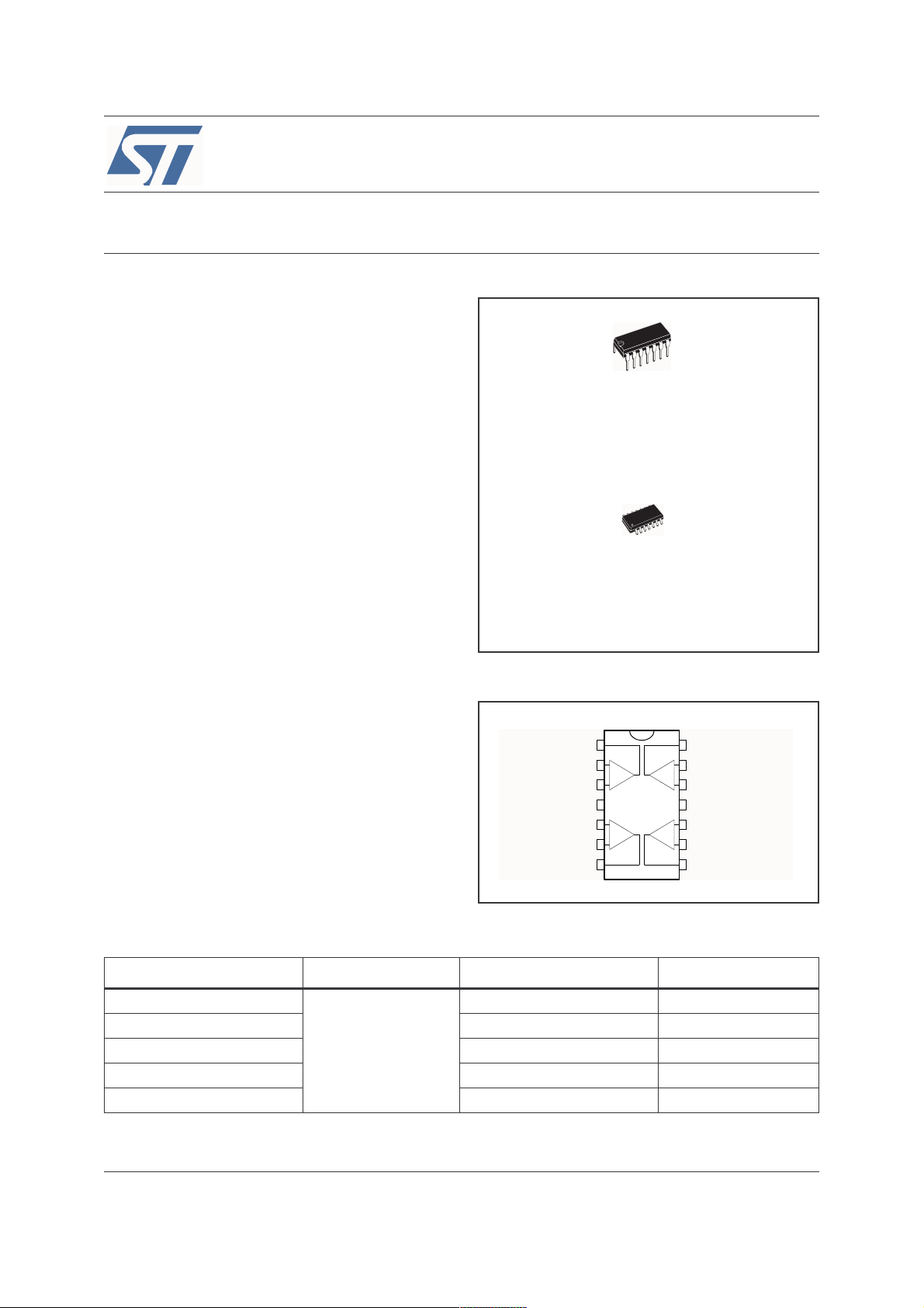
TS914
N
DIP-14
(Plastic Package)
Description
The TS914 is a rail-to-rail CMOS quad operational
amplifier designed to operate with a single or dual
(Plastic Micropackage)
D
SO-14
supply voltage.
The input voltage range V
supply rails V
CC
+
and V
CC
includes the two
icm
-
.
Pin Connections (top view)
The output reaches:
■ V
■ V
-
+50mV, V
CC
-
+350mV, V
CC
This product offers a broad supply voltage
operating range from 2.7V to 16V and a supply
current of only 200µA/amp (V
Source and sink output current capability is
typically 40mA (at V
+
-50mV, with RL = 10kΩ
CC
+
-350mV, with RL = 600Ω
CC
= 3V).
CC
= 3V), fixed by an internal
CC
Output 1
Inverting Input 1
Non-inverting Input 1
V
CC
Non-inverting Input 2
Inverting Input 2
Output 2
1
2
-
+
3
+
4
5
+
-
6
7
14
13
-
+
12
11
10
+
9
8
Output 4
Inverting Input 4
Non-inverting Input 4
-
V
CC
Non-inverting Input 3
Inverting Input 3
Output 3
limitation circuit.
Order Code
Part Number Temperature Range Package Packaging
TS914IN
TS914ID/IDT SO-4 Tube or Tape & Reel
TS914AIN DIP14 Tube
-40, +125°C
TS914AID/AIDT SO-4 Tube or Tape & Reel
TS914IYD/IYDT/ AIYD/AIYDT SO14 (automotive grade level) Tube or Tape & Reel
DIP14 Tube
Rev 3
June 2005 1/17
www.st.com
17
Page 2
1 Absolute Maximum Ratings TS914
1 Absolute Maximum Ratings
Table 1. Key parameters and their absolute maximum ratings
Symbol Parameter Value Unit
(3)
(1)
(2)
CC
+
+0.3V.
18 V
±18 V
-0.3 to 18 V
V
T
T
1. All voltages values, except differential voltage are with respect to network ground terminal.
2. Differential voltagesare non-inverting input terminal with respect to the inverting input terminal.
3. The magnitude of input and output voltages must never exceed V
Supply voltage
CC
Vid
Differential Input Voltage
V
Input Voltage
i
I
Current on Inputs ±50 mA
in
I
Current on Outputs ±130 mA
o
Operating Free Air Temperature Range
oper
TS914I/AI -40 to + 125
Storage Temperature -65 to +150 °C
stg
Table 2. Operating conditions
Symbol Parameter Value Unit
V
V
Supply voltage 2.7 to 16 V
CC
Common Mode Input Voltage Range
icm
V
CC
-
-0.2 to V
CC
+
+0.2
°C
V
2/17
Page 3
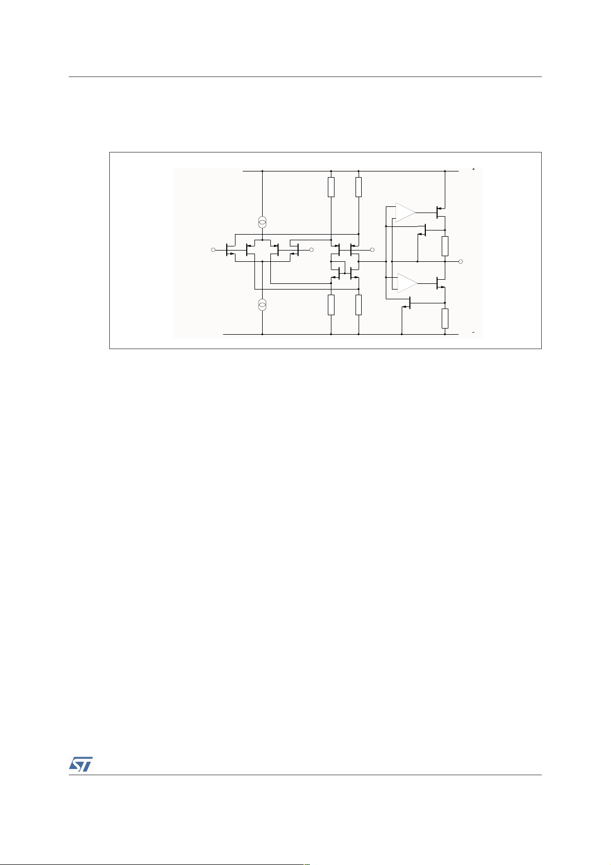
TS914 2 Typical Application Information
2 Typical Application Information
Figure 1. Typical application information
V
CC
Internal
Non-inverting
Input
Inverting
Input
Vref
Output
V
CC
3/17
Page 4
3 Electrical Characteristics TS914
3 Electrical Characteristics
Table 3. V
CC
+
= 3V, V
-
= 0V, RL, CL connected to V
cc
CC/2
, T
= 25°C (unless otherwise
amb
specified)
Symbol Parameter Min. Typ. Max. Unit
V
io
∆V
io
I
io
I
ib
I
CC
CMR
SVR
A
vd
Input Offset Voltage (Vic = Vo = V
TS914
TS914A
T
≤ T
min.
amb
≤ T
max.
TS914
TS914A
Input Offset Voltage Drift 5 µV/°C
Input Offset Current
T
≤ T
amb
≤ T
min.
Input Bias Current
T
≤ T
amb
≤ T
min.
(1)
max.
1)
max.
Supply Current (per amplifier, A
T
≤ T
amb
≤ T
max.
min.
Common Mode Rejection Ratio
V
= 0 to 3V, Vo = 1.5V
ic
Supply Voltage Rejection Ratio (V
V
)
CC/2
Large Signal Voltage Gain (RL = 10kΩ, Vo = 1.2V to 1.8V)
T
≤ T
amb
≤ T
max.
min.
)
CC/2
= 1, no load)
VCL
+
= 2.7 to 3.3V, Vo =
CC
1
1 150
200 300
70 dB
80 dB
3
10
2
10
5
12
7
100
200
300
400
mV
pA
pA
µA
V/mV
High Level Output Voltage (Vid = 1V)RL = 10kΩ
R
= 600Ω
L
R
V
OH
= 100Ω
L
T
min.
R
= 600Ω
L
≤ T
amb
≤ T
max.RL
= 10kΩ
2.9
2.2
2.8
2.1
Low Level Output Voltage (Vid = -1V)RL = 10kΩ
R
= 600Ω
L
V
OL
R
= 100Ω
L
T
min.
R
= 600Ω
L
≤ T
amb
≤ T
max.RL
= 10kΩ
2.97
2.7
2
50
300
900
100
600
mV
150
900
Output Short Circuit Current (Vid = ±1V)
Source (V
I
o
Sink (V
GBP
Gain Bandwith Product
(A
VCL
Slew Rate
SR
(A
VCL
φm Phase Margin 30
Equivalent Input Noise Voltage (R
en
V
/
O1
V
1. Maximum values including unavoidable inaccuracies of the industrial test
Channel Separation (f = 1kHz) 120 dB
O2
= VCC)
o
+
o
= V
CC
)
= 100, RL = 10kΩ, CL = 100pF, f = 100kHz)
= 1, RL = 10kΩ, CL = 100pF, Vi = 1.3V to 1.7V)
= 100Ω, f = 1kHz)
s
40
mA
40
0.8 MHz
0.5 V/µs
Degree
30 nV/√Hz
V
s
4/17
Page 5
3 Electrical Characteristics TS914
Table 4. V
CC
+
= 5V, V
-
= 0V, RL, CL connected to V
cc
CC/2
, T
= 25°C (unless otherwise
amb
specified)
Symbol Parameter Min. Typ. Max. Unit
V
io
∆V
io
I
io
I
ib
I
CC
CMR
SVR
A
vd
Input Offset Voltage (Vic = Vo = V
TS914
TS914A
T
≤ T
min.
amb
≤ T
max.
TS914
TS914A
Input Offset Voltage Drift 5 µV/°C
≤ T
≤ T
(1)
max.
1)
max.
Input Offset Current
T
≤ T
min.
amb
Input Bias Current
T
≤ T
min.
amb
Supply Current (per amplifier, A
T
≤ T
amb
≤ T
max.
min.
Common Mode Rejection Ratio
V
= 1.5 to 3.5V, Vo = 2.5V
ic
Supply Voltage Rejection Ratio (V
Large Signal Voltage Gain (RL = 10kΩ, Vo = 1.5V to 3.5V)
T
≤ T
amb
≤ T
max.
min.
)
CC/2
= 1, no load)
VCL
+
= 3 to 5V, Vo = V
CC
CC/2
10
5
mV
12
7
100
1
200
1 150
300
230 350
450
pA
pA
µA
85 dB
)
10
80 dB
40
7
V/mV
High Level Output Voltage (Vid = 1V)RL = 10kΩ
R
= 600Ω
L
V
OH
R
= 100Ω
L
T
R
= 600Ω
L
min.
≤ T
amb
≤ T
max.RL
= 10kΩ
4.85
4.20
4.8
4.1
Low Level Output Voltage (Vid = -1V)RL = 10kΩ
R
= 600Ω
L
V
GBP
R
OL
I
o
= 100Ω
L
T
≤ T
R
= 600Ω
L
min.
amb
≤ T
max.RL
= 10kΩ
Output Short Circuit Current (Vid = ±1V)Source (Vo = VCC)
Sink (V
o
= V
CC
+
)
Gain Bandwith Product
(A
= 100, RL = 10kΩ, CL = 100pF, f = 100kHz)
VCL
Slew Rate
SR
(A
= 1, RL = 10kΩ, CL = 100pF, Vi = 1V to 4V)
VCL
φm Phase Margin 30
Equivalent Input Noise Voltage (R
en
V
/
O1
V
1. Maximum values including unavoidable inaccuracies of the industrial test
Channel Separation (f = 1kHz) 120 dB
O2
= 100Ω, f = 1kHz)
s
4.95
4.65
3.7
50
350
1400
100
680
V
mV
150
900
60
60
mA
1MHz
0.8 V/µs
Degree
s
30 nV/√Hz
5/17
Page 6
3 Electrical Characteristics TS914
Table 5. V
CC
+
= 10V, V
= 0V, RL, CL connected to V
DD
CC/2
, T
= 25°C (unless otherwise
amb
specified)
Symbol Parameter Min. Typ. Max. Unit
∆V
V
Input Offset Voltage (Vic = Vo = V
TS914
V
TS914A
io
T
≤ T
min.
amb
≤ T
max.
TS914
TS914A
Input Offset Voltage Drift 5 µV/°C
io
Input Offset Current
I
io
T
≤ T
≤ T
amb
amb
≤ T
≤ T
min.
Input Bias Current
I
ib
T
min.
Common Mode Input Voltage Range
icm
(1)
max.
1)
max.
CC/2
)
10
5
12
7
100
1
200
1150
300
V
DD
- 0.2 to V
CC
+
0.2
Common Mode Rejection Ratio
V
CMR
SVR
A
vd
= 3 to 7V, Vo = 5V
ic
V
= 0 to 10V, Vo = 5V
ic
Supply Voltage Rejection Ratio (V
+
= 5 to 10V, Vo = V
CC
Large Signal Voltage Gain (RL = 10kΩ, Vo = 2.5V to 7.5V)
T
≤ T
amb
≤ T
max.
min.
CC/2
)
90
75
90 dB
151060
V/mV
High Level Output Voltage (Vid = 1V)RL = 10kΩ
9.85
9.95
9
9.35
7.8
9.8
9
50
650
2300
60 mA
400 600
1.4 MHz
1V/µs
180
800
150
900
700
V
OH
V
OL
I
o
I
CC
GBP
SR
R
= 600Ω
L
R
= 100Ω
L
T
≤ T
R
= 600Ω
L
min.
amb
≤ T
max.RL
= 10kΩ
Low Level Output Voltage (Vid = -1V)RL = 10kΩ
R
= 600Ω
L
R
= 100Ω
L
T
≤ T
R
= 600Ω
L
min.
amb
≤ T
max.RL
= 10kΩ
Output Short Circuit Current (Vid = ±1V)
Supply Current (per amplifier, A
T
≤ T
amb
≤ T
max.
min.
= 1, no load)
VCL
Gain Bandwith Product
= 100, RL = 10kΩ, CL = 100pF, f = 100kHz)
(A
VCL
Slew Rate
(A
= 1, RL = 10kΩ, CL = 100pF, Vi = 2.5V to 7.5V)
VCL
φm Phase Margin 40 Degrees
Equivalent Input Noise Voltage (R
en
= 100Ω, f = 1kHz)
s
30 nV/√Hz
Total Harmonic Distortion
THD
= 1, RL = 10kΩ, CL = 100pF, Vo = 4.75V to 5.25V, f =
VCL
0.02 %
(A
1kHz)
C
Input Capacitance 1.5 pF
in
R
Input Resistance >10 Tera Ω
in
V
O1/VO2
1. Maximum values including unavoidable inaccuracies of the industrial test
Channel Separation (f = 1kHz) 120 dB
mV
pA
pA
V
dB
V
mV
µA
6/17
Page 7
3 Electrical Characteristics TS914
Table 6. V
+
= 3V, VCC- = 0V, RL, CL connected to V
CC
CC/2
, T
= 25°C (unless otherwise
amb
specified)
Symbol Conditions Value Unit
V
A
I
CC
V
icm
V
OH
V
OL
I
sink
I
source
GBP
SR
io
vd
RL = 10kΩ
No load, per operator 100 µA
RL = 600Ω
RL = 60Ω
VO = 3V
VO = 0V
= 10kΩ, CL = 100pF
R
L
R
= 10kΩ, CL = 100pF
L
0mV
10 V/mV
-0.2 to 3.2 V
2.96 V
300 mV
40 mA
40 mA
0.8 MHz
0.3 V/µs
φm Phase Margin 30 Degrees
7/17
Page 8

3 Electrical Characteristics TS914
Figure 2. Supply current (each amplifier)
vs supply voltage
600
A)
m
CC
500
T = 25°C
amb
A = 1
VCL
V = V / 2
O CC
400
300
200
SUPPLY CURRENT, I (
100
0 4 8 12 16
SUPPLY VOLTAGE, V (V)
CC
Figure 4. Low level output voltage vs low level
output current
5
T = 25 C
amb
4
OL
V = -100mV
°
id
V = +5V
CC
Figure 3. High level output voltage vs high
level output current
5
T = 25 C
amb
OH
4
V = 100mV
id
°
V = +5V
CC
3
2
V = +3V
1
OUTPUT VOLTAGE, V (V)
CC
0
-70 -40 -20 0
OUTPUT CURRENT, I (mA)
OH
Figure 5. Input bias current vs temperature
100
V = 10V
CC
V = 5V
ib
i
No load
3
V = +3V
CC
2
1
OUTPUT VOLTAGE, V (V)
0 30 50 70 90
OUTPUT CURRENT, I (mA)
OL
Figure 6. High level output voltage vs high
level output current
T = 25 C
20
16
OH
12
8
4
OUTPUT VOLTAGE, V (V)
0
amb
V = 100mV
°
id
V = +16V
CC
V = +10V
CC
-70 -40 -20 0
OUTPUT CURRENT, I (mA)
OH
10
INPUT BIAS CURRENT, I (pA)
1
25 50 75 100 125
TEMPERATURE, T ( C)
amb
°
Figure 7. Low level output voltage vs low level
output current
10
T = 25 C
amb
8
OL
6
4
2
OUTPUT VOLTAGE, V (V)
0
V = -100mV
°
id
V = 16V
CC
V = 10V
CC
30 50 70 90
OUTPUT CURRENT, I (mA)
OL
8/17
Page 9

3 Electrical Characteristics TS914
6
6
Figure 8. Gain and phase vs frequency Figure 9. Gain bandwidth product vs supply
voltage
50
40
30
PHASE
20
T = 25°C
V = 10V
GAIN (dB)
R = 10k
10
C = 100pF
A = 100
0
-10
23
10
amb
CC
L
L
VCL
W
10
Gain
Bandwidth
Product
4
10510
FREQUENCY, f (Hz)
GAIN
10
Phase
Margin
6
10
7
0
45
90
135
180
PHASE (Degrees)
1800
1400
T = 25°C
amb
R = 10k
L
C = 100pF
L
W
1000
600
200
GAIN BANDW. PROD., GBP (kHz)
0 4 8 12 16
SUPPLY VOLTAGE, V (V)
CC
Figure 10. Phase margin vs supply voltage Figure 11. Gain and phase vs frequency
60
T = 25°C
amb
R = 10k
50
f
40
L
C = 100pF
W
L
30
20
PHASE MARGIN, m (Degrees)
0 4 8 12 1
SUPPLY VOLTAGE, V (V)
CC
50
40
30
T = 25°C
20
V = 10V
GAIN (dB)
R = 600
10
C = 100pF
A = 100
0
-
10
23
10
PHASE
amb
CC
L
L
VCL
10
GAIN
W
Gain
Bandwidth
Product
10
4
10
5
FREQUENCY, f (Hz)
Phase
Margin
10
6
10
7
0
45
90
135
180
PHASE (Degrees)
Figure 12. Gain bandwidth product vs supply
voltage
1800
T = 25°C
amb
1400
R = 600
C = 100pF
1000
600
200
GAIN BANDW. PROD., GBP (kHz)
0 4 8 12 16
9/17
W
L
L
SUPPLY VOLTAGE, V (V)
CC
Figure 13. Phase margin vs supply voltage
60
T = 25°C
amb
R = 600
50
f
40
L
C = 100pF
L
30
20
PHASE MARGIN, m (Degrees)
0 4 8 12 1
W
SUPPLY VOLTAGE, V (V)
CC
Page 10

3 Electrical Characteristics TS914
Figure 14. Input voltage noise vs frequency
150
100
50
EQUIVALENT INPUT
VOLTAGE NOISE (nV/VHz)
0
10 100
V
CC
T
amb
R
S
1000
FREQUENCY (Hz)
= 10V
= 25°C
= 100
W
10000
10/17
Page 11

4 Macromodels TS914
4 Macromodels
Note: Please consider following remarks before using this macromodel:
All models are a trade-off between accuracy and complexity (i.e. simulation time).
Macromodels are not a substitute to breadboarding; rather, they confirm the validity of a design
approach and help to select surrounding component values.
A macromodel emulates the NOMINAL performance of a TYPICAL device within SPECIFIED
OPERATING CONDITIONS (i.e. temperature, supply voltage, etc.). Thus the macromodel is
often not as exhaustive as the datasheet, its goal is to illustrate the main parameters of the
product.
Data issued from macromodels used outside of its specified conditions (Vcc, Temperature, etc)
or even worse: outside of the device operating conditions (Vcc, Vicm, etc) are not reliable in any
way.
Applies to : TS914I,AI,BI (VCC = 3V)
** Standard Linear Ics Macromodels, 1993.
** CONNECTIONS :
* 1 INVERTING INPUT
* 2 NON-INVERTING INPUT
* 3 OUTPUT
* 4 POSITIVE POWER SUPPLY
* 5 NEGATIVE POWER SUPPLY
.SUBCKT TS914_3 1 3 2 4 5 (analog)
********************************************************** .MODEL
MDTH D IS=1E-8 KF=6.564344E-14 CJO=10F * INPUT STAGE
CIP 2 5 1.000000E-12
CIN 1 5 1.000000E-12
EIP 10 5 2 5 1
EIN 16 5 1 5 1
RIP 10 11 6.500000E+00
RIN 15 16 6.500000E+00
RIS 11 15 1.271505E+01
DIP 11 12 MDTH 400E-12
DIN 15 14 MDTH 400E-12
VOFP 12 13 DC 0.000000E+00
VOFN 13 14 DC 0
IPOL 13 5 4.000000E-05
CPS 11 15 2.125860E-08
DINN 17 13 MDTH 400E-12
VIN 17 5 0.000000e+00
DINR 15 18 MDTH 400E-12
VIP 4 18 0.000000E+00
FCP 4 5 VOFP 5.000000E+00
FCN 5 4 VOFN 5.000000E+00
* AMPLIFYING STAGE
FIP 5 19 VOFP 2.750000E+02
FIN 5 19 VOFN 2.750000E+02
RG1 19 5 1.916825E+05
RG2 19 4 1.916825E+05
CC 19 29 2.200000E-08
HZTP 30 29 VOFP 1.3E+03
HZTN 5 30 VOFN 1.3E+03
DOPM 19 22 MDTH 400E-12
DONM 21 19 MDTH 400E-12
11/17
Page 12

4 Macromodels TS914
HOPM 22 28 VOUT 3800
VIPM 28 4 150
HONM 21 27 VOUT 3800
VINM 5 27 150
EOUT 26 23 19 5 1
VOUT 23 5 0
ROUT 26 3 75
COUT 3 5 1.000000E-12
DOP 19 68 MDTH 400E-12
VOP 4 25 1.724
HSCP 68 25 VSCP1 0.8E8
DON 69 19 MDTH 400E-12
VON 24 5 1.7419107
HSCN 24 69 VSCN1 0.8E+08
VSCTHP 60 61 0.0875
** VSCTHP = le seuil au dessus de vio
* 500
** c.a.d 275U-000U dus a l’offset
DSCP1 61 63 MDTH 400E-12
VSCP1 63 64 0
ISCP 64 0 1.000000E-8
DSCP2 0 64 MDTH 400E-12
DSCN2 0 74 MDTH 400E-12
ISCN 74 0 1.000000E-8
VSCN1 73 74 0
DSCN1 71 73 MDTH 400E-12
VSCTHN 71 70 -0.55
** VSCTHN = le seuil au dessous de vio
* 2000
** c.a.d -375U-000U dus a l’offset
ESCP 60 0 2 1 500
ESCN 70 0 2 1 -2000
.ENDS
12/17
Page 13

4 Macromodels TS914
Macromodels
Applies to : TS914I,AI,BI (V
** Standard Linear Ics Macromodels, 1993.
** CONNECTIONS :
* 1 INVERTING INPUT
* 2 NON-INVERTING INPUT
* 3 OUTPUT
* 4 POSITIVE POWER SUPPLY
* 5 NEGATIVE POWER SUPPLY
* 6 STANDBY
.SUBCKT TS914_5 1 3 2 4 5 (analog)
**********************************************************.MODEL
MDTH D IS=1E-8 KF=6.564344E-14 CJO=10F * INPUT STAGE
CIP 2 5 1.000000E-12
CIN 1 5 1.000000E-12
EIP 10 5 2 5 1
EIN 16 5 1 5 1
RIP 10 11 6.500000E+00
RIN 15 16 6.500000E+00
RIS 11 15 7.322092E+00
DIP 11 12 MDTH 400E-12
DIN 15 14 MDTH 400E-12
VOFP 12 13 DC 0.000000E+00
VOFN 13 14 DC 0
IPOL 13 5 4.000000E-05
CPS 11 15 2.498970E-08
DINN 17 13 MDTH 400E-12
VIN 17 5 0.000000e+00
DINR 15 18 MDTH 400E-12
VIP 4 18 0.000000E+00
FCP 4 5 VOFP 5.750000E+00
FCN 5 4 VOFN 5.750000E+00
ISTB0 5 4 500N
* AMPLIFYING STAGE
FIP 5 19 VOFP 4.400000E+02
FIN 5 19 VOFN 4.400000E+02
RG1 19 5 4.904961E+05
RG2 19 4 4.904961E+05
CC 19 29 2.200000E-08
HZTP 30 29 VOFP 1.8E+03
HZTN 5 30 VOFN 1.8E+03
DOPM 19 22 MDTH 400E-12
DONM 21 19 MDTH 400E-12
HOPM 22 28 VOUT 3800
VIPM 28 4 230
HONM 21 27 VOUT 3800
VINM 5 27 230
EOUT 26 23 19 5 1
VOUT 23 5 0
ROUT 26 3 82
COUT 3 5 1.000000E-12
DOP 19 68 MDTH 400E-12
VOP 4 25 1.724
HSCP 68 25
VSCP1 0.8E+08
DON 69 19 MDTH 400E-12
VON 24 5 1.7419107
= 5V)
CC
13/17
Page 14

4 Macromodels TS914
HSCN 24 69
VSCN1 0.8E+08
VSCTHP 60 61 0.0875
** VSCTHP = le seuil au dessus de vio
* 500
** c.a.d 275U-000U dus a l’offset
DSCP1 61 63 MDTH 400E-12
VSCP1 63 64 0
ISCP 64 0 1.000000E-8
DSCP2 0 64 MDTH 400E-12
DSCN2 0 74 MDTH 400E-12
ISCN 74 0 1.000000E-8
VSCN1 73 74 0
DSCN1 71 73 MDTH 400E-12
VSCTHN 71 70 -0.55
** VSCTHN = le seuil au dessous de vio
* 2000
** c.a.d -375U-000U dus a l’offset
ESCP 60 0 2 1 500
ESCN 70 0 2 1 -2000
.ENDS
14/17
Page 15

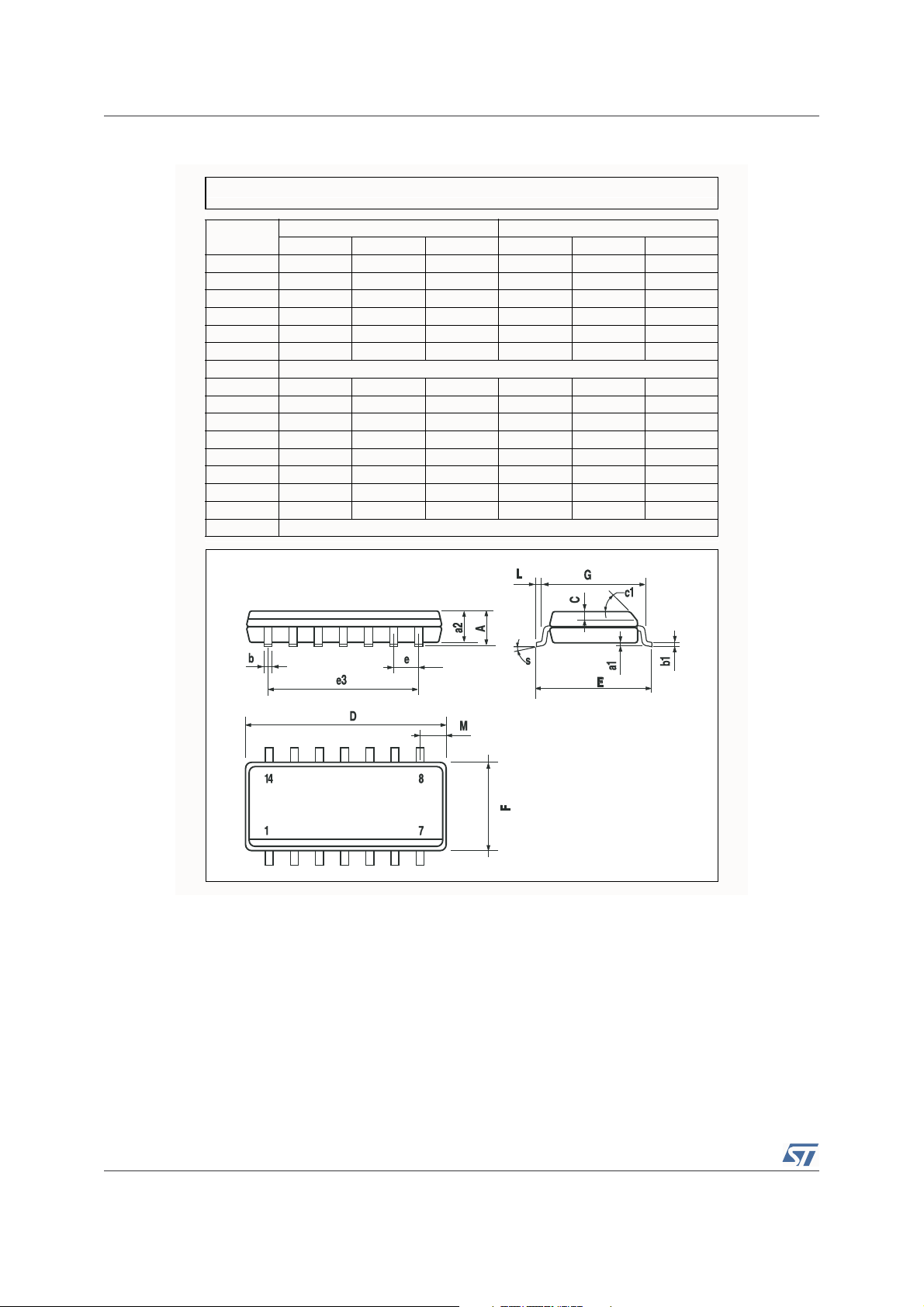
5 Package Mechanical Data TS914
5 Package Mechanical Data
In order to meet environmental requirements, ST offers these devices in ECOPACK® packages.
These packages have a Lead-free second level interconnect. The category of second level
interconnect is marked on the package and on the inner box label, in compliance with JEDEC
Standard JESD97. The maximum ratings related to soldering conditions are also marked on
the inner box label. ECOPACK is an ST trademark. ECOPACK specifications are available at:
www.st.com
5.1 DIP-14 Package
.
Plastic DIP-14 MECHANICAL DATA
DIM.
a1 0.51 0.020
B 1.39 1.65 0.055 0.065
b 0.5 0.020
b1 0.25 0.010
D 20 0.787
E 8.5 0.335
e 2.54 0.100
e3 15.24 0.600
F 7.1 0.280
I 5.1 0.201
L 3.3 0.130
Z 1.27 2.54 0.050 0.100
MIN. TYP MAX. MIN. TYP. MAX.
mm. inch
15/17
P001A
Page 16
5 Package Mechanical Data TS914
5.2 SO-14 Package
SO-14 MECHANICAL DATA
DIM.
A 1.75 0.068
a1 0.1 0.2 0.003 0.007
a2 1.65 0.064
b 0.35 0.46 0.013 0.018
b1 0.19 0.25 0.007 0.010
C 0.5 0.019
c1 45˚ (typ.)
D 8.55 8.75 0.336 0.344
E 5.8 6.2 0.228 0.244
e 1.27 0.050
e3 7.62 0.300
F 3.8 4.0 0.149 0.157
G 4.6 5.3 0.181 0.208
L 0.5 1.27 0.019 0.050
M 0.68 0.026
S˚ (max.)
MIN. TYP MAX. MIN. TYP. MAX.
mm. inch
8
16/17
PO13G
Page 17

6 Revision History TS914
6 Revision History
Date Revision Changes
Dec 2001 1 First Release
Nov 2004 2 Vio max on 1st page from 2mV to 5mV
June 2005 2 PIPAP references inserted in the datasheet see table order code p1
Information furnished is believed to be accurate and reliable. However, STMicroelectronics assumes no responsibility for the consequences
of use of such information nor for any infringement of patents or other rights of third parties which may result from its use. No license is
granted by implication or otherwise under any patent or patent rights of STMicroelectronics. Specifications mentioned in this publication are
subject to change without notice. This publication supersedes and replaces all information previously supplied. STMicroelectronics products
are not authorized for use as critical components in life support devices or systems without express written approval of STMicroelectronics.
The ST logo is a registered trademark of STMicroelectronics.
All other names are the property of their respective owners
© 2005 STMicroelectronics - All rights reserved
STMicroelectronics group of companies
Australia - Belgium - Brazil - Canada - China - Czech Republic - Finland - France - Germany - Hong Kong - India - Israel - Italy - Japan -
Malaysia - Malta - Morocco - Singapore - Spain - Sweden - Switzerland - United Kingdom - United States of America
www.st.com
17/17
 Loading...