

TS507
High precision rail-to-rail operational amplifier
Features
■ Ultra low offset voltage: 25 µV typ, 100 µV max
■ Rail-to-rail input/output voltage swing
■ Operating from 2.7 V to 5.5 V
■ High speed: 1.9 MHz
■ 45° phase margin with 100 pF
■ Low consumption: 0.8 mA at 2.7 V
■ Very large signal voltage gain: 131 dB
■ High power supply rejection ratio: 105 dB
■ Very high ESD protection 5kV (HBM)
■ Latch-up immunity
■ Available in SOT23-5 micropackage
Applications
■ Battery-powered applications
■ Portable devices
■ Signal conditioning
■ Medical instrumentation
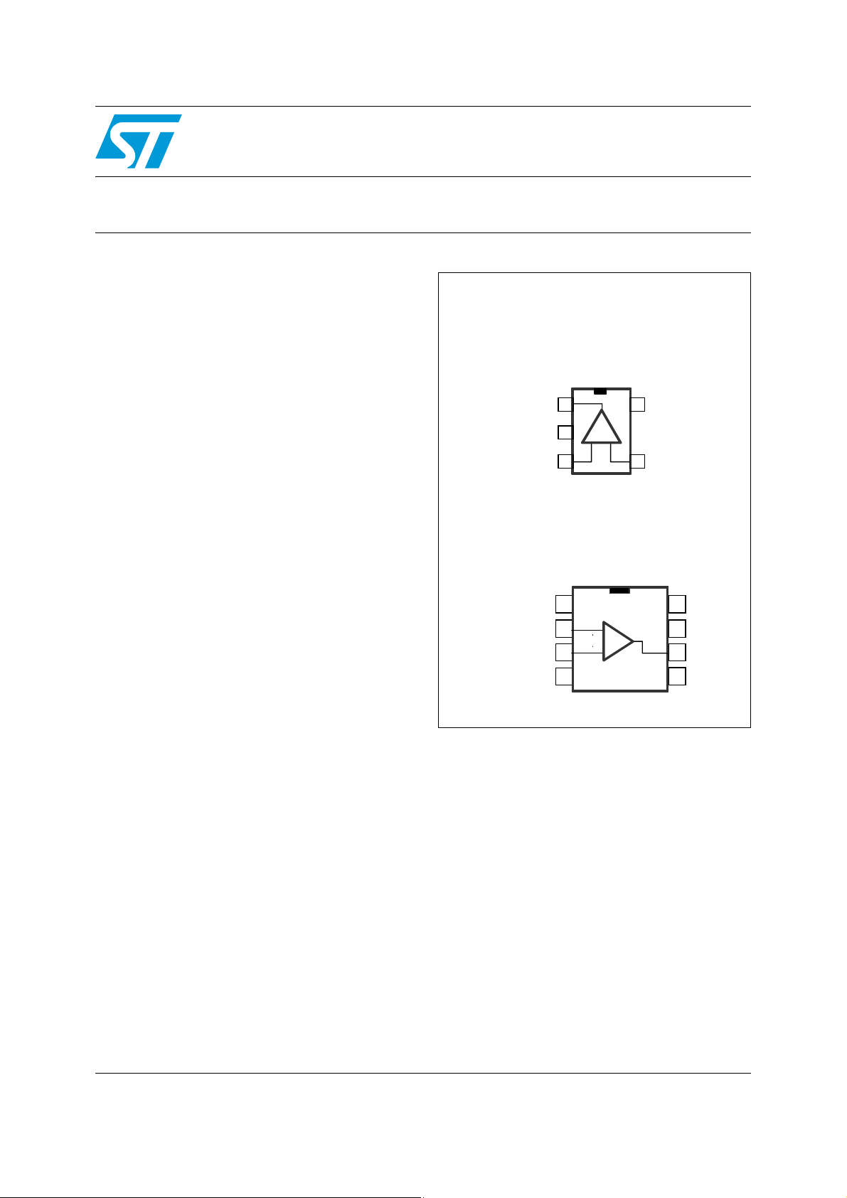
Pin connections (top view)
SOT23-5
VCC
Output
Output
Non Inverting Input Inverting Input
Non Inverting Input Inverting Input
VDD
VDD
1
1
2
2
3
3
VCC
5
5
4
4
SO-8
N.C.
N.C.
Inverting Input
Inverting Input
Non Inverting Input
Non Inverting Input
VDD
VDD
1
1
_
2
2
3
3
4
4
_
+
+
N.C.
N.C.
8
8
VCC
VCC
7
7
Output
Output
6
6
N.C.
N.C.
5
5
Description
The TS507 is a high performance rail-to-rail input
and output amplifier with very low offset voltage.
This amplifier uses a new trimming technique that
yields ultra low offset volt ages without any need
for external zeroing.
The circuit offers very stable electrical
characteristics over the entire supply voltage
range, and is particularly intended for automotive
and industrial applications.
The TS507 is housed in the space-saving 5-pin
SOT23 package, making it well suited for batterypowered systems. This micropackage simplifies
the PC board design because of its ability to be
placed in tight spaces (external dimensions are
2.8 mm x 2.9 mm).
April 2008 Rev 5 1/20
www.st.com
20

Contents TS507
Contents
1 Absolute maximum ratings and operating conditions . . . . . . . . . . . . . 3
2 Electrical characteristics . . . . . . . . . . . . . . . . . . . . . . . . . . . . . . . . . . . . . 4
3 Application note . . . . . . . . . . . . . . . . . . . . . . . . . . . . . . . . . . . . . . . . . . . 15
3.1 Out-of-the-loop compensation technique . . . . . . . . . . . . . . . . . . . . . . . . . 15
3.2 In-the-loop-compensation technique . . . . . . . . . . . . . . . . . . . . . . . . . . . . 16
4 Package information . . . . . . . . . . . . . . . . . . . . . . . . . . . . . . . . . . . . . . . . 17
4.1 SOT23-5 package information . . . . . . . . . . . . . . . . . . . . . . . . . . . . . . . . . 17
4.2 SO-8 package . . . . . . . . . . . . . . . . . . . . . . . . . . . . . . . . . . . . . . . . . . . . . 18
5 Ordering information . . . . . . . . . . . . . . . . . . . . . . . . . . . . . . . . . . . . . . . 19
6 Revision history . . . . . . . . . . . . . . . . . . . . . . . . . . . . . . . . . . . . . . . . . . . 19
2/20

TS507 Absolute maximum ratings and operating conditions
1 Absolute maximum ratings and operating conditions
Table 1. Absolute maximum ratings (AMR)
Symbol Parameter Value Unit
(3)
(1)
(7)
(2)
(6)
(8)
(4) (5)
6V
±2.5 V
VDD-0.3 to VCC+0.3 V
250
°C/W
125
81
°C/W
40
5kV
300 V
2kV
V
CC
V
id
V
in
T
stg
R
thja
R
thjc
T
ESD
Supply voltage
Differential input voltage
Input voltage
Storage temperature -65 to +150 °C
Thermal resistance junction to ambient
SOT23-5
SO-8
Thermal resistance junction to case
SOT23-5
SO-8
Maximum junction temperature 150 °C
j
HBM: human body model
MM: machine model
CDM: charged device model
Latch-up immunity class A
1. Value with respect to VDD pin.
2. Differential voltages are the non-inverting input terminal with respect to the inverting input terminal.
3. VCC-Vin must not exceed 6V and Vin must not exceed 6V.
4. Short-circuits can cause excessive heating and destructive dissipation.
5. R
6. Human body model: A 100 pF capacitor is charged to the specified voltage, then discharged through a
7. Machine model: A 200pF capacitor is charged to the specified voltage, then discharged directly between
8. Charged device model: all pins and the package are charged together to the specified voltage and then
Table 2. Operating conditions
are typical values.
thja/c
1.5 kΩ resistor between two pins of the device. This is done for all couples of connected pin combinations
while the other pins are floating.
two pins of the device with no external series resistor (internal resistor < 5 Ω). This is done for all couples of
connected pin combinations while the other pins are floating.
discharged directly to the ground through only one pin. This is done for all pins.
Symbol Parameter Value Unit
V
V
Supply voltage
CC
Common mode input voltage range VDD to V
icm
Differential input voltage
V
id
(1)
(2)
2.7 to 5.5 V
CC
±2.5 V
Operating free air temperature range
T
oper
TS507C
TS507I
1. Value with respect to VDD pin.
2. Differential voltages are the non-inverting input terminal with respect to the inverting input terminal.
0 to +85
-40 to +125
V
°C
3/20

Electrical characteristics TS507
2 Electrical characteristics
Table 3. Electrical characteristics at VCC=+5V, VDD=0V, V
R
connected to VCC/2 (unless otherwise specified)
L
icm=VCC
(1)
/2, T
amb
=25°C,
Symbol Parameter Conditions Min. Typ. Max. Unit
DC performance
V
V
ΔV
CMRR
PSRR
A
V
CC-VOH
V
Input offset voltage
io
/ΔtVio drift vs. temperature T
io
I
Input bias current
ib
I
Input offset current
io
Common mode rejection ratio
20 log (ΔV
icm
Power supply rejection ratio
20 log (ΔV
Large signal voltage gain
vd
CC
High level output voltage drop
Low level output voltage
OL
(2)
/ΔVio)
/ΔVio)
= 0 to 3.8V, T=25°C
icm
TS507C full temp range
TS507I full temp range
V
= 0V to 5V, T=25°C
icm
TS507C full temp range
TS507I full temp range
< Top < T
min
max
T = 25°C
TS507C full temp range
TS507I full temp range
T = 25°C
TS507C full temp range
TS507I full temp range
from 0V to 3.8V, T=25°C
V
icm
TS507C full temp range
TS507I full temp range
V
from 0V to 5V 96
icm
from 2.7V to 5.5V,
V
CC
V
icm=vcc
/2, T=25°C
TS507C full temp range
TS507I full temp range
R
= 10kΩ, V
L
= 0.5V to 4.5V
out
Full temp range
= 600Ω, T=25°C
R
L
TS507C full temp range
TS507I full temp range
= 10kΩ, T=25°C
R
L
Full Temp range
= 600Ω, T=25°C
R
L
TS507C full temp range
TS507I full temp range
= 10kΩ, T=25°C
R
L
Full temp range
94
94
91
91
90
89
99
98
25 100
250
400
450
550
750
1µV/°C
870
75
110
225
35
50
115
105
131
67 95
110
120
415
15
64 90
110
125
415
15
µV
µV
nA
nA
dB
dB
dB
mV
mV
4/20

TS507 Electrical characteristics
Table 3. Electrical characteristics at VCC=+5V, VDD=0V, V
R
connected to VCC/2 (unless otherwise specified)
L
icm=VCC
(1)
/2, T
amb
(continued)
=25°C,
Symbol Parameter Conditions Min. Typ. Max. Unit
V
= V
out
I
sink
TS507C full temp range
TS507I full temp range
I
out
I
source
V
= VDD, Vid=1V, T=25°C
out
TS507C full temp range
TS507I full temp range
No load, V
I
Supply current (per operator)
CC
(2)
=0 to 5V, T=25°C
V
icm
Full temp range
CC, Vid
out=VCC
=-1V, T=25°C
/2,
74
60
53
90
77
70
104
128
0.85 1.15
1.25
Dynamic performance
=2kΩ, CL= 100pF,
R
GBP Gain bandwidth product
φ
G
Phase margin RL = 2kΩ, CL=100pF 45 Degrees
m
Gain margin RL = 2kΩ, CL=100pF 10 dB
m
SR Slew rate
L
f = 100kHz
= 2kΩ, CL=100pF,
R
L
V
= 1.25V to 3.75V, 10% to
out
1.9 MHz
0.6 V/µs
90%
e
THD+eNTHD + noise
1. All parameter limits at temperatures different from 25° C are guaranteed by correlation.
2. Measurements done at 4 V
Equivalent input noise voltage f = 1kHz 12 nV/√Hz
N
Equivalent input noise current f = 10kHz 1.2 pA/√Hz
i
N
values: V
icm
icm
=0 V, V
f=1kHz, G=1, R
V
=3.5V
out
=3.8 V, V
icm
pp
=2kΩ, V
L
=4.2 V, V
icm
icm
icm
=2V,
=5 V.
0.0003 %
mA
mA
5/20
Electrical characteristics TS507
Table 4. Electrical characteristics at VCC=+3.3V, VDD=0V, V
R
connected to VCC/2 (unless otherwise specified)
L
icm=VCC
(1)
/2, T
amb
= 25°C,
Symbol Parameter Conditions Min. Typ. Max. Unit
DC performance
V
V
io
ΔV
io
I
ib
I
io
CMRR
Input offset voltage
(2)
Vio drift vs. temperature T
Input bias current
Input offset current
Common mode rejection ratio
20 log (ΔV
icm
/ΔVio)
= 0 to 2.1V, T=25°C
icm
TS507C full temp range
TS507I full temp range
= 0V to 3.3V, T=25°C
V
icm
TS507C full temp range
TS507I full temp range
< Top < T
min
max
T = 25°C
TS507C full temp range
TS507I full temp range
T = 25°C
TS507C full temp range
TS507I full temp range
from 0V to 2.1V 115 dB
V
icm
25 100
250
400
450
550
750
1µV/°C
670
75
145
225
40
45
µV
µV
nA
nA
A
Large signal voltage gain RL = 10kΩ, V
vd
VCC-VOHHigh level output voltage drop
V
I
I
Low level output voltage
OL
I
sink
out
I
source
Supply current (per operator)
CC
= 600Ω, T=25°C
R
L
TS507C full temp range
TS507I full temp range
= 10kΩ, T=25°C
R
L
Full temp range
R
= 600Ω, T=25°C
L
TS507C full temp range
TS507I full temp range
= 10kΩ, T=25°C
R
L
Full temp range
V
= V
out
CC, Vid
TS507C full temp range
TS507I full temp range
V
= VDD, Vid=1V, T=25°C
out
TS507C full temp range
TS507I full temp range
(2)
No load, V
V
icm
out=VCC
=0 to 3.3V, T=25°C
Full temp range
= 0.5V to 2.8V 127 dB
out
59 85
100
110
415
15
57 80
100
115
415
15
=-1V, T=25°C
33
48
26
22
37
56
32
29
/2,
0.81 1.1
1.2
mV
mV
mA
mA
6/20

TS507 Electrical characteristics
Table 4. Electrical characteristics at VCC=+3.3V, VDD=0V, V
R
connected to VCC/2 (unless otherwise specified)
L
icm=VCC
(1)
(continued)
/2, T
amb
= 25°C,
Symbol Parameter Conditions Min. Typ. Max. Unit
Dynamic performance
=2kΩ, CL= 100pF,
R
GBP Gain bandwidth product
φ
G
Phase margin RL = 2kΩ, CL=100pF 45 Degrees
m
Gain margin RL = 2kΩ, CL=100pF 10 dB
m
SR Slew rate
e
Equivalent input noise voltage f = 1kHz 12 nV/√Hz
N
THD+eNTHD + noise
1. All parameter limits at temperatures different from 25° C are guaranteed by correlation.
2. Measurements done at 4 V
values: V
icm
icm
L
f = 100kHz
R
= 2kΩ, CL=100pF,
L
V
= 0.5V to 2.8V, 10% to 90%
out
f=1KHz, G=1, R
V
=1.15V, V
icm
=0 V, V
=2.1 V, V
icm
L
=1.8V
out
=2.5 V, V
icm
=2kΩ,
pp
=3.3 V.
icm
1.9 MHz
0.6 V/µs
0.0004 %
7/20

Electrical characteristics TS507
Table 5. Electrical characteristics at VCC=+2.7V VDD=0V, V
R
connected to VCC/2 (unless otherwise specified)
L
icm=VCC
(1)
/2, T
amb
=25°C,
Symbol Parameter Conditions Min. Typ. Max. Unit
DC performance
V
V
io
ΔV
io
I
ib
I
io
CMRR
Input offset voltage
(2)
Vio drift vs. temperature T
Input bias current
Input offset current
Common mode rejection ratio
20 log (ΔV
icm
/ΔVio)
= 0 to 1.9V, T=25°C
icm
TS507C full temp range
TS507I full temp range
= 0V to 2.7V, T=25°C
V
icm
TS507C full temp range
TS507I full temp range
< Top < T
min
max
T = 25°C
TS507C full temp range
TS507I full temp range
T = 25°C
TS507C full temp range
TS507I full temp range
from 0V to 1.5V 115 dB
V
icm
25 100
250
400
450
550
750
1µV/°C
870
75
160
225
45
45
µV
µV
nA
nA
A
Large signal voltage gain RL = 10kΩ, V
vd
VCC-VOHHigh level output voltage drop
V
I
I
Low level output voltage
OL
I
sink
out
I
source
Supply current (per operator)
CC
= 600Ω, T=25°C
R
L
TS507C full temp range
TS507I full temp range
= 10kΩ, T=25°C
R
L
Full temp range
R
= 600Ω, T=25°C
L
TS507C full temp range
TS507I full temp range
= 10kΩ, T=25°C
R
L
Full temp range
V
= V
out
CC, Vid
TS507C full temp range
TS507I full temp range
V
= VDD, Vid=1V, T=25°C
out
TS507C full temp range
TS507I full temp range
(2)
No load, V
V
icm
out=VCC
=0 to 2.7V, T=25°C
Full temp range
= 0.5V to 2.2V 126 dB
out
57 85
100
105
415
15
57 80
100
115
415
15
=-1V, T=25°C
20
30
15
13
22
35
19
17
/2,
0.79 1.1
1.2
mV
mV
mA
mA
8/20

TS507 Electrical characteristics
Table 5. Electrical characteristics at VCC=+2.7V VDD=0V, V
R
connected to VCC/2 (unless otherwise specified)
L
icm=VCC
(1)
(continued)
/2, T
amb
=25°C,
Symbol Parameter Conditions Min. Typ. Max. Unit
Dynamic performance
=2kΩ, CL= 100pF,
R
GBP Gain bandwidth product
φ
G
Phase margin RL = 2kΩ, CL=100pF 45 Degrees
m
Gain margin RL = 2kΩ, CL=100pF 11 dB
m
SR Slew rate
e
Equivalent input noise voltage f = 1kHz 12 nV/√Hz
N
THD+eNTHD + noise
1. All parameter limits at temperatures different from 25° C are guaranteed by correlation.
2. Measurements done at 4 V
values: V
icm
icm
L
f = 100kHz
R
= 2kΩ, CL=100pF,
L
V
= 0.5V to 2.2V, 10% to 90%
out
f=1KHz, G=1, R
V
=0.85V, V
icm
=0 V, V
=1.5 V, V
icm
L
=1.2V
out
=1.9 V, V
icm
=2kΩ,
pp
=2.7 V.
icm
1.9 MHz
0.6 V/µs
0.0005 %
9/20

Electrical characteristics TS507
Figure 1. Input offset voltage distribution for
V
≤ VCC-1.2V at T=25°C
icm
30
Vio distribution at T=25°C for 0V<=Vicm<=Vcc-1.2V
25
20
15
10
Population %
5
0
-120 -100 -80 -60 -40 -20 0 20 40 60 80 100 120
Input offset voltage (µV)
Figure 3. Input offset voltage distribution vs.
temperature for V
700
600
500
400
300
200
100
0
-100
Vio (µV)
-200
-300
-400
-500
-600
-700
-50 -40 -30 -20 -10 0 10 20 30 40 50 60 70 80 90 100 110 120 130
Vcc-0.8V<=Vicm <= Vcc
Temperature (°C)
≥ VCC-0.8V
icm
Figure 2. Input offset voltage distribution vs.
temperature for V
400
350
300
250
200
150
100
50
0
-50
Vio (µV)
-100
-150
-200
-250
-300
-350
-400
-50 -40 -30 -20 -10 0 10 20 30 40 50 60 70 80 90 100 110 120 130
0V<=Vicm<=Vcc-1.2V
Temperature (°C)
≤ VCC-1.2V
icm
Figure 4. Input offset voltage distribution for
V
≤ VCC-1.2V at T=25°C after HTB
icm
45
Vio distribution at T=25°C for 0V<=Vicm<=Vcc-1.2V
40
after HTB (1000 hours at 125°C)
35
30
25
20
15
Population %
10
5
0
-100 -80 -60 -40 -20 0 20 40 60 80 100
Input offset voltage (µV)
Figure 5. Input offset voltage distribution for
V
≤ VCC-1.2V at T=25°C after THB
icm
35
Vio distribution at T=25°C for 0V<=Vicm<=Vcc-1.2V
30
after THB (1000 hours at 85°C, humidity 85%)
25
20
15
Population %
10
5
0
-120 -100 -80 -60 -40 -20 0 20 40 60 80 100 120
Input offset voltage (µV)
10/20
Figure 6. Input offset voltage vs. input
common mode voltage at T=25°C
4040
2020
Vcc=3.3V
00
-20-20
Vcc=5.5V
Vcc=5V
-40-40
-60-60
Input Offset Voltage (μV)
-80-80
-100-100
-2.5-2.5 -2 .0-2.0 -1.5-1.5 -1.0-1.0 -0.5-0.5 0.00.0
Vcc=2.7V
Vicm-Vcc (V)

TS507 Electrical characteristics
Figure 7. Supply current vs. input common
mode voltage in closed loop
configuration at V
1.01.0
0.8
0.7
0.50.5
0.3
Vcc=5V
Supply Current (mA)
Closed loop
0.2
0.00.0
001122334455
Input common mode voltage (V)
T=-40°C
CC
T=25°C
=5V
T=125°C
Figure 9. Supply current vs. input common
mode voltage in follower
configuration at V
1.01.0
0.8
0.7
0.50.5
T=25°C
CC
=2.7V
T=125°C
T=-40°C
Figure 8. Supply current vs. supply v olta ge at
V
icm=VCC
1.01.0
0.8
0.7
0.50.5
0.3
Supply Current (mA)
0.2
0.00.0
001122334455
/2
T=125°C
T=25°C
T=-40°C
Vicm=Vcc/2
Supply voltage (V)
Figure 10. Supply current vs. input common
mode voltage in follower
configuration at VCC=5V
1.01.0
0.8
0.7
0.50.5
T=-40°C
T=125°C
T=25°C
0.3
Supply Current (mA)
0.2
0.00.0
0.00.0 0.50.5 1.01.0 1.51.5 2.02.0 2.52.5
Follower configuration
Vcc=2.7V
Input Common Mode Voltage (V)
Figure 11. Output current vs. supply volta ge at
V
icm=VCC
150
Source
125
Vid = 1V
100100
T=125°C
75
50
25
00
-25
-50
Output Current (mA)
-75
-100-100
Sink
-125
Vid = -1V
-150
3.03.0 3.53.5 4.04.0 4.54.5 5.05.0 5.55.5
/2
T=25°C
T=125°C
T=25°C
Supply voltage (V)
T=-40°C
Vicm=Vcc/2
T=-40°C
0.3
Supply Current (mA)
0.2
0.00.0
001122334455
Follower configuration
Vcc=5V
Input Common Mode Voltage (V)
Figure 12. Output current vs. output voltage at
VCC=2.7V
4040
35
30
25
2020
T=25°C
15
10
5
00
-5
-10
-15
Output Current (mA)
-20-20
Sink
-25
Vid=-1V
-30
-35
-40-40
0.00.0 0.50.5 1.01.0 1.51.5 2.02.0 2.52.5
T=125°C
Vcc=2.7V
T=-40°C
Output Voltage (V)
T=125°C
T=-40°C
Source
Vid=1V
T=25°C
11/20

Electrical characteristics TS507
Figure 13. Output current vs. output v oltage at
V
=5V
CC
150
125
100100
75
T=125°C
50
25
00
-25
-50
Output Current (mA)
-75
Sink
-100-100
Vid=-1V
-125
-150
0.00.0 1.01.0 2.02.0 3.03.0 4.04.0 5.05.0
T=-40°C
Output Voltage (V)
Vcc=5V
T=25°C
T=125°C
T=25°C
Source
Vid=1V
T=-40°C
Figure 15. Voltage gain and phase vs.
frequency at V
=5V and V
CC
icm
=2.5V
at T=25°C
Gain (dB)
50
4040
30
2020
10
00
-10
Vcc=5V, V icm=2.5V, G= -100
-20-20
Rl=2kOhms, Vrl=Vcc/2
-30
Tamb=25°C
-40-40
-50
4
10
Gain
5
10
Frequency (Hz)
10
Phase
Cl=100pF
Cl=230pF
6
180
150
120
90
60
30
0
-30
Phase (°)
-60
-90
-120
-150
-180
7
10
Figure 14. Positive and negative slew rate vs.
supply voltage
1.01.0
0.80.8
0.60.6
0.40.4
0.20.2
Vin : from 0.5V to Vcc-0.5V
0.00.0
SR : calculated from 10% to 90%
-0.2-0.2
-0.4-0.4
-0.6-0.6
Positive and Negative Slew Rate (V/µs)
-0.8-0.8
-1.0-1.0
2.0 2.5 3 .03.03.54.04.55.05.0 5.5 6.0
Positive s lew ra te
Neg ative sle w ra te
Supp ly Vo lt ag e (V )
T=-40°C
T=125°C
T=25°C
T=-40°C
T=25°C
T=125°C
Figure 16. Voltage gain and phase vs.
frequency at VCC=5V and V
icm
=2.5V
at T=-40°C
Gain (dB)
50
4040
30
2020
10
00
-10
-20-2 0
Vcc=5V, Vicm=2.5V, G= -100
-30
Rl=2kOhms, Cl=100pF, Vrl=Vcc/2
-40-4 0
Tamb=-40°C
-50
4
10
5
10
10
Frequency (Hz)
Phase
Gain
6
180
150
120
90
60
30
0
-30
Phase (°)
-60
-90
-120
-150
-180
7
10
Figure 17. Voltage gain and phase vs.
frequency at V
=5V and V
CC
icm
=2.5V
at T=125°C
50
4040
30
2020
10
00
Gain (dB)
-10
-20-20
Vcc=5V, Vicm=2.5V, G= -100
-30
Rl=2kOhms, Cl=100pF, Vrl=Vcc/2
Tamb=125°C
-40-40
-50
4
10
5
10
Frequency (Hz)
10
Phase
Gain
6
12/20
180
150150
120120
9090
6060
3030
0
-30-30
Phase (°)
-60-60
-90-90
-120-120
-150-150
-180
7
10
Figure 18. Closed loop gain in voltage follower
configuration for different
capacitive load at T=25°C
2020
TS507 :
Vcc = 5 V
10
= 2,5 V
V
icm
T = 25 °C
R
= 10 kΩ
L
00
-10
Gain (dB)
-20-2 0
-30
-40-4 0
10k 100k 1M 10M
Gain without C
Gain w ith CL=300 pF
Ga in w ith CL=550 pF
Frequency (Hz)
L

TS507 Electrical characteristics
Figure 19. Gain margin according the output
load, at V
1E-6
1E-7
1E-8
1E-9
1E-10
Load Capacitor (F)
30 dB
1E-11
1E-12
1 10 100 1k 10k 100k 1M 10M
=5V and T=25°C
CC
UNSTABLE
STABLE
Load Resistor (Ω)
0 dB
10 dB
20 dB
Vcc = 5 V
V
= 2,5 V
icm
= 25 °C
T
amb
Figure 21. G ai n margin vs. o utp ut cu rre n t, at
V
=5V and T=25°C
CC
20.020.0
17.5
15.015.0
12.5
10.010.0
7.5
Gain Margin (dB)
5.05.0
2.5
0.00.0
-2.5
550 pF
-4-4 -3 -2-2 -1 00122344
Recomm en ded area
Output Current (mA)
100 pF
300 pF
Vcc = 5 V
V
= 2,5 V
icm
T
= 25 °C
amb
R
= 2 kΩ
L
Figure 20. Phase margin according the output
load, at VCC=5V and T=25°C
1E-6
1E-7
0 °
1E-8
10 °
1E-9
1E-10
Load Capacitor (F)
1E-11
1E-12
20 °
1 10 100 1k 10k 100k 1M 10M
30 °
40 °
UNSTABLE
STABLE
50 °
Load Resistor (Ω)
Vcc = 5 V
= 2,5 V
V
icm
= 25 °C
T
amb
Figure 22. Phase margin vs. output current, at
VCC=5V and T=25°C
70
6060
50
4040
550 pF
30
2020
Phase Margin (°)
10
00
-10
-4-4 -3 -2-2 -1 00122344
Recomm e nded area
100 pF
Output Current (mA)
300 pF
Vcc = 5 V
V
= 2,5 V
icm
T
= 25 °C
amb
R
= 2 kΩ
L
Figure 23. Phase and gain margins vs
capacitive load at = 25°C
30
2020
10
00
-10
Gain (dB)
-20-20
-30
-40-40
10p 100p 1n 10n
Load Capacitor (F)
Vcc = 5 V
V
icm
T
amb
R
L
Gain Margin
Phase Margin
= 2,5 V
= 25 °C
= 2 kΩ
75
50
25
0
-25
-50
-75
-100
Figure 24. Distortion + noise vs. output
voltage
0.1000
Vcc=5V
0.0100
Phase (°)
THD + N (%)
0.0010
0.0001
f=1kHz
Rl=2kOhms
Gain=1
BW=22kHz
Vicm=(Vcc-1V)/2
0.01 0.1 1
Output Voltage (Vpp)
13/20
Vcc=3.3V
Vcc=2.7V

Electrical characteristics TS507
Figure 25. Distortion + noise vs. frequency Figure 26. Noise vs. frequency
0.01
Vout=Vcc-1.5Vpp
Rl=2kOhms
Gain=1
BW =80kHz
Vicm=(Vcc-1V)/2
1E-3
THD + N (%)
1E-4
10 100 1000 10000
Vcc=2.7V
Frequency (Hz)
Vcc=5V
Vcc=3.3V
1000
100
10
Vcc=5V, Vicm= 2.5V, T am b=2 5°C
Input equivalent noise density (nV/VHz)
1
1 10 100 1000 10000
Frequency (Hz)
14/20

TS507 Application note
3 Application note
An application note, based on the TS507, describes three compensation techniques for
solving stability issues when driving large capacitive loads. Two of them are briefly explained
here. For more details, refer to the application note on www.st.com. To find it, do a keyword
search for AN2653.
3.1 Out-of-the-loop compensation technique
The first technique, named the out-of-the-loop compensation, uses an isolation resistor,
R
, added in series between the output of the amplifier and its load (see Figure 27). The
OL
resistor isolates the op-amp feed back network from the capacitive load. This compensation
method is effective, but the drawback is a limitation on the accuracy of V
the resistive load value.
Figure 27. Out-of-the-loop compensation schematics
depending on
out
To help implement the compensation, the abacus give n in Figure 28 to Figure 29 provide the
R
value to choose fo r a given CL and phase/gain margins. These abacus are plotted in
OL
the case of a voltage follower configuration with a load resistor of 10 kΩ at 25°C.
Figure 28. Gain margin abacus : serial resistor
to be added in a voltage follower
configuration at 25°C
100
OL
10
1
Compensation Resistor R
0.1
0.01
10p 100p 1n 10n 100n 1µ 10µ
8 dB
4 dB
12 dB
0 dB
16 dB
UNSTABLE
Load Capacitor (F)
STABLE
Vcc = 5 V
V
T = 25 °C
RL = 10 kΩ
= 2,5 V
icm
Figure 29. Phase margin abacus : serial
resistor to be added in a voltage
follower configuration at 25°C
100
OL
10
1
UNSTABLE
Compensation Resistor R
0.1
0.01
10p 100p 1n 10n 100n 1µ 10µ
Load Capacitor (F)
STABLE
Vcc = 5 V
V
icm
T = 25 °C
R
L
20 °
10 °
= 2,5 V
= 10 kΩ
30 °
0 °
15/20

Application note TS507
3.2 In-the-loop-compensation technique
The second technique is called the in-the-loop-compensation technique, because the
additional components (a resistor and a capacitor) use d to impro v e the st ability are inserted
in the feedback loop (see Figure 30).
Figure 30. In-the-loop compensation schematics
This compensation method allows, by a good choice of compensation components, to
compensate the original pole (caused by the capacitive load), and thus to improve stability.
The main drawback of this circuit is the reduction of the output swing, because the isolation
resistor is in the signal path.
Table 6 helps you to choose the best compensation components for different ranges of load
capacitors (and with R
Table 6. Best compensation components for different load capac itor ranges in
voltage follower configuration for TS507 (with R
Load capacitor
range
10 pF to 100 pF 1 250 17 55
100 pF to 1 nF 1 250 16 42
1 nF to 10 nF 1 630 11 27
1. Parameter guaranteed by design at 25°C.
= 10 kΩ) in voltage follower configuration.
L
(kΩ)C
R
IL
IL
(pF)
Minimum gain
margin (dB)
= 10 kΩ)
L
(1)
Minimum phase
margin
(degree)
(1)
16/20

TS507 Package information
4 Package information
In order to meet environmental requirements, STMicroelectronics offe rs these devices in
ECOPACK
®
packages. These packages have a lead-free second le vel interconnect. The
category of second level interconnect is marke d on the pa ckage and on the inner box label,
in compliance with JEDEC Standard JESD97. The maximum ratings related t o soldering
conditions are also marked on the inner box label. ECOPACK is an STMicroelectronics
trademark. ECOPACK specifications are available at: www.st.com
4.1 SOT23-5 package information
Figure 31. SOT23-5 package mechanical drawing
.
Table 7. SOT23-5 package mechanical data
Dimensions
Ref.
Min. Typ. Max. Min. Typ. Max.
A 0.90 1.45 35.4 57.1
A1 0.00 0.15 0.00 5.9
A2 0.90 1.30 35.4 51.2
b 0.35 0.50 13.7 19.7
C 0.09 0.20 3.5 7.8
D 2.80 3.00 110.2 118.1
E 2.60 3.00 102.3 118.1
E1 1.50 1.75 59.0 68.8
e 0.95 37.4
e1 1.9 74.8
L 0.35 0.55 13.7 21.6
Millimeters Mils
17/20

Package information TS507
4.2 SO-8 package
Figure 32. SO-8 package mechanical drawing
Table 8. SO-8 package mechanical data
Dimensions
Ref.
Min. Typ. Max. Min. Typ. Max.
A1.750.069
A1 0.10 0.25 0.004 0.010
A2 1.25 0.049
b 0.28 0.48 0.011 0.019
c 0.17 0.23 0.007 0.010
D 4.80 4.90 5.00 0.189 0.193 0.197
E 5.80 6.00 6.20 0.228 0.236 0.244
E1 3.80 3.90 4.00 0.150 0.154 0.157
e 1.27 0.050
h 0.25 0.50 0.010 0.020
L 0.40 1.27 0.016 0.050
k1°8°1°8°
ccc 0.10 0.004
Millimeters Inches
18/20

TS507 Ordering information
5 Ordering information
Table 9. Orde r codes
Order code
Temperature
TS507ID
TS507IDT
TS507IYD
TS507IYDT
(1)
(1)
-40°C to 125°C
TS507ILT
TS507IYLT
(1)
-40°C to 125°C
TS507CD
TS507CDT
0°C to 85°C
TS507CLT SOT23-5
1. Qualification and characterization according to AEC Q100 and Q003 or equivalent, advanced screening
according to AEC Q001 & Q 002 or equivalent are on-going.
2. All information related to the SOT23-5 package is subject to change without notice.
6 Revision history
Table 10. Document revision history
range
Package Packing Marking
SO-8
Tube or
SO-8
Tape & reel
(Automotive grade)
SO-8
(2)
(2)
(2)
Tape & reel K131
Tape & reel K137
Tube or
Tape & reel
Tape & reel K136
SOT23-5
SOT23-5
(Automotive grade)
TS507I
TS507Y
TS507C
Date Revision Changes
01-Oct-2004 1 Preliminary data release for product in development.
02-May-2006 2 Update preliminary data release for product in development.
15-Dec-2006 3 F irst public release.
03-May-2007 4 Automotive grade products added.
Electrical characteristics curves for Bode and AC stability added and
08-Apr-2008 5
updated.
Application note section added.
19/20

TS507
Please Read Carefully:
Information in this document is provided solely in connection with ST products. STMicroelectronics NV and its subsidiaries (“ST”) reserve the
right to make changes, corrections, modifications or improvements, to this document, and the products and services described herein at any
time, without notice.
All ST products are sold pursuant to ST’s terms and conditions of sale.
Purchasers are solely res ponsibl e fo r the c hoic e, se lecti on an d use o f the S T prod ucts and s ervi ces d escr ibed he rein , and ST as sumes no
liability whatsoever relati ng to the choice, selection or use of the ST products and services described herein.
No license, express or implied, by estoppel or otherwise, to any intellectual property rights is granted under this document. If any part of this
document refers to any third pa rty p ro duc ts or se rv ices it sh all n ot be deem ed a lice ns e gr ant by ST fo r t he use of su ch thi r d party products
or services, or any intellectua l property c ontained the rein or consi dered as a warr anty coverin g the use in any manner whats oever of suc h
third party products or servi ces or any intellectual property contained therein .
UNLESS OTHERWISE SET FORTH IN ST’S TERMS AND CONDITIONS OF SALE ST DISCLAIMS ANY EXPRESS OR IMPLIED
WARRANTY WITH RESPECT TO THE USE AND/OR SALE OF ST PRODUCTS INCLUDING WITHOUT LIMITATION IMPLIED
WARRANTIES OF MERCHANTABILITY, FITNESS FOR A PARTICUL AR PURPOS E (AND THEIR EQUIVALE NTS UNDER THE LAWS
OF ANY JURISDICTION), OR INFRINGEMENT OF ANY PATENT, COPYRIGHT OR OTHER INTELLECTUAL PROPERTY RIGHT.
UNLESS EXPRESSLY APPROVED IN WRITING BY AN AUTHORIZED ST REPRESENTATIVE, ST PRODUCTS ARE NOT
RECOMMENDED, AUTHORIZED OR WARRANTED FOR USE IN MILITARY, AIR CRAFT, SPACE, LIFE SAVING, OR LIFE SUSTAINING
APPLICATIONS, NOR IN PRODUCTS OR SYSTEMS WHERE FAILURE OR MALFUNCTION MAY RESULT IN PERSONAL INJ URY,
DEATH, OR SEVERE PROPERTY OR ENVIRONMENTAL DAMAGE. ST PRODUCTS WHICH ARE NOT SPECIFIED AS "AUTOMOTIVE
GRADE" MAY ONLY BE USED IN AUTOMOTIVE APPLICATIONS AT USER’S OWN RISK.
Resale of ST products with provisions different from the statements and/or technical features set forth in this document shall immediately void
any warranty granted by ST fo r the ST pro duct or serv ice describe d herein and shall not cr eate or exten d in any manne r whatsoever , any
liability of ST.
ST and the ST logo are trademarks or registered trademarks of ST in various countries.
Information in this document su persedes and replaces all information previously s upplied.
The ST logo is a registered trademark of STMicroelectronics. All other names are the property of their respective owners.
© 2008 STMicroelectronics - All rights reserved
STMicroelectronics group of compan ie s
Australia - Belgium - Brazil - Canada - China - Czech Republic - Finland - France - Germany - Hong Kong - India - Israel - Italy - Japan -
Malaysia - Malta - Morocco - Singapore - Spain - Sweden - Switzerland - United Kingdom - United States of America
www.st.com
20/20
 Loading...