

Features
TS4995
1.2W fully differential audio power amplifier
with selectable standby and 6db fixed gain
■ Differential inputs
■ 90dB PSRR @ 217Hz with grounded inputs
■ Operating from Vcc = 2.5V to 5.5V
■ 1.2W rail to rail output power @ Vcc=5V,
THD+N=1%, F=1kHz, with 8Ω load
■ 6dB integrated fixed gain
■ Ultra-low consumption in standby mode (10nA)
■ Selectable standby mode (active low or active
high)
■ Ultra-fast startup time: 10ms typ. at Vcc=3.3V
■ Available in 9-bump flip-chip (300mm bump
diameter)
■ Ultra-low pops&clicks
Description
The TS4995 is an audio power amplifier capable
of delivering 1.2W of continuous RMS output
power into an 8Ω load at 5V. Thanks to its
differential inputs, it exhibits outstanding noise
immunity.
An external standby mode control reduces the
supply current to less than 10nA. A STBY MODE
pin allows the standby pin to be active HIGH or
LOW. An internal thermal shutdown protection is
also provided, making the device capable of
sustaining short-circuits.
The TS4995 features an internal fixed gain at 6dB
which reduces the number of external
components on the application board.
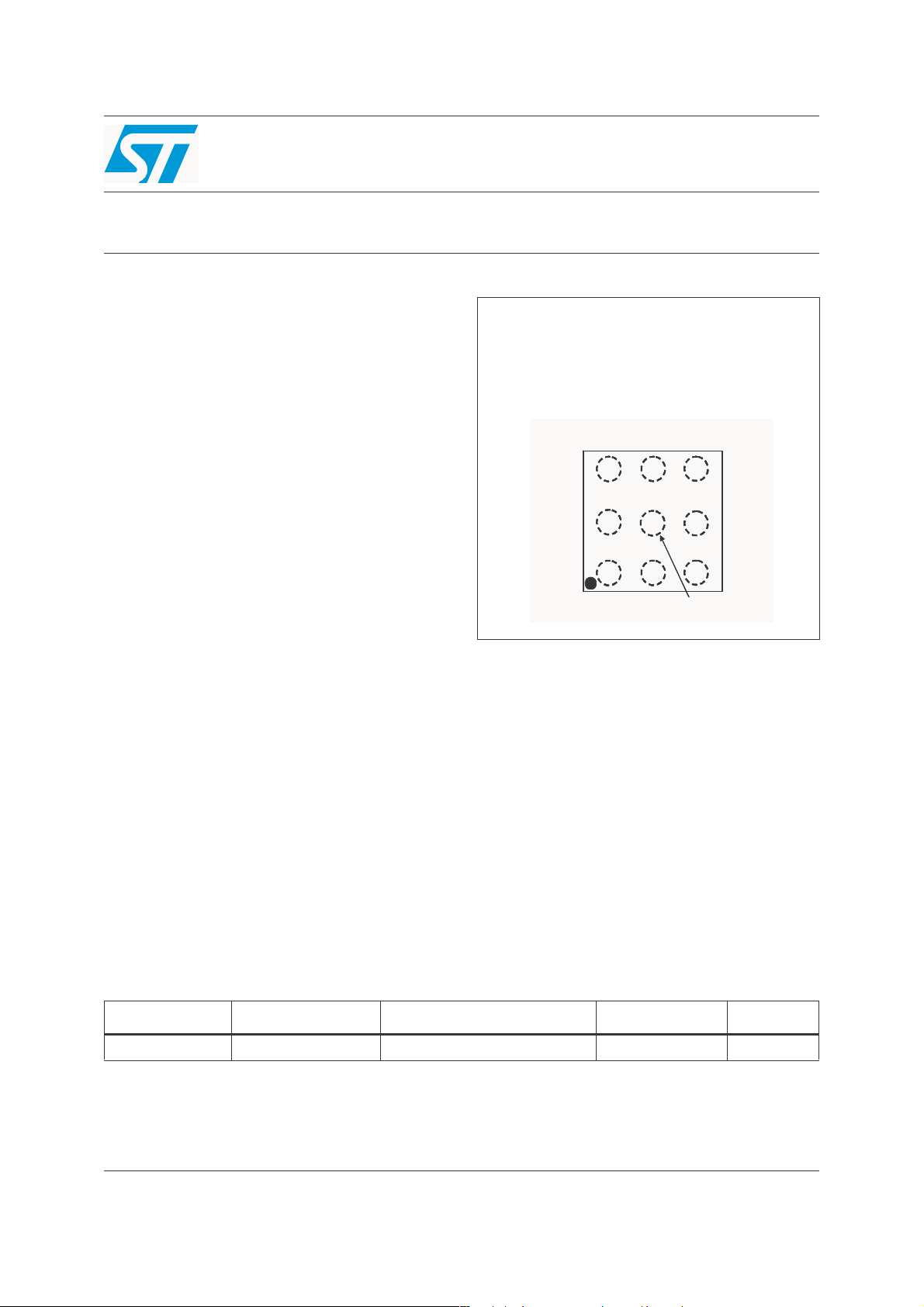
TS4995 - Flip-Chip9
Pin connections (top view)
Gnd
Gnd
V
V
Bypass Stdby
Bypass Stdby
V
V
765
765
O-
O-
8
8
IN+
IN+
1
1
9
9
2
2
V
V
CC
CC
V
V
O+
O+
4
4
V
V
3
3
IN-
IN-
Stdby Mode
Stdby Mode
The device is equipped with Common Mode
Feedback circuitry allowing outputs to be always
biased at Vcc/2 regardless of the input common
mode voltage.
The TS4995 has been designed for high quality
audio applications such as mobile phones and
requires few external components.
Applications
■ Mobile phones (cellular / cordless)
■ PDAs
■ Laptop / notebook computers
■ Portable audio devices
Device summary table
Part Number Temperature Range Package Packing Marking
TS4995EIJT -40°C to +85°C Lead free flip-chip9 Tape & Reel 95
June 2006 Rev. 1 1/24
www.st.com
24

Contents TS4995
Contents
1 Absolute maximum ratings & operating conditions . . . . . . . . . . . . . . . 3
2 Typical application schematic . . . . . . . . . . . . . . . . . . . . . . . . . . . . . . . . . 4
3 Electrical characteristics . . . . . . . . . . . . . . . . . . . . . . . . . . . . . . . . . . . . . 5
4 Application information . . . . . . . . . . . . . . . . . . . . . . . . . . . . . . . . . . . . . 16
4.1 Differential configuration principle . . . . . . . . . . . . . . . . . . . . . . . . . . . . . . . 16
4.2 Common mode feedback loop limitations . . . . . . . . . . . . . . . . . . . . . . . . . 16
4.3 Low frequency response . . . . . . . . . . . . . . . . . . . . . . . . . . . . . . . . . . . . . . 16
4.4 Power dissipation and efficiency . . . . . . . . . . . . . . . . . . . . . . . . . . . . . . . . 17
4.5 Decoupling of the circuit . . . . . . . . . . . . . . . . . . . . . . . . . . . . . . . . . . . . . . 18
4.6 Wake-up Time: TWU . . . . . . . . . . . . . . . . . . . . . . . . . . . . . . . . . . . . . . . . 19
4.7 Shutdown time . . . . . . . . . . . . . . . . . . . . . . . . . . . . . . . . . . . . . . . . . . . . . 19
4.8 Pop performance . . . . . . . . . . . . . . . . . . . . . . . . . . . . . . . . . . . . . . . . . . . 19
4.9 Single-ended input configuration . . . . . . . . . . . . . . . . . . . . . . . . . . . . . . . 19
5 Package mechanical data . . . . . . . . . . . . . . . . . . . . . . . . . . . . . . . . . . . . 21
5.1 9-bump flip-chip package . . . . . . . . . . . . . . . . . . . . . . . . . . . . . . . . . . . . . 21
6 Revision history . . . . . . . . . . . . . . . . . . . . . . . . . . . . . . . . . . . . . . . . . . . 23
2/24
TS4995 Absolute maximum ratings & operating conditions
1 Absolute maximum ratings & operating conditions
Table 1. Absolute maximum ratings (AMR)
Symbol Parameter Value Unit
V
CC
V
T
oper
T
stg
T
R
thja
P
diss
ESD
i
j
Supply voltage
Input voltage
Operating free air temperature range -40 to + 85 °C
Storage temperature -65 to +150 °C
Maximum junction temperature 150 °C
Thermal resistance junction to ambient
Power dissipation Internally limited W
Machine model 200 V
Human body model 1.5 kV
Latch-up Latch-up immunity 200 mA
- Lead temperature (soldering, 10sec) 260 °C
1. All voltage values are measured with respect to the ground pin.
2. The magnitude of input signal must never exceed VCC + 0.3V / GND - 0.3V.
3. Device is protected in case of over temperature by a thermal shutdown activated at 150°C.
Table 2. Operating conditions
Symbol Parameter Value Unit
V
Supply voltage 2.5 to 5.5 V
CC
Standby Mode Voltage Input:
V
SM
Standby Active LOW
Standby Active HIGH
Standby Voltage Input:
V
STB
Device ON (V
Device OFF (V
T
R
R
1. The minimum current consumption (I
temperature range.
Thermal Shutdown Temperature 150 °C
SD
Load Resistor ≥ 8 Ω
L
Thermal Resistance Junction to Ambient 100 °C/W
thja
(1)
(2)
(3)
=GND) or Device OFF (VSM=VCC)
SM
=GND) or Device ON (VSM=VCC)
SM
) is guaranteed when V
STANDBY
6V
GND to V
CC
200 °C/W
=GND
V
SM
V
SM=VCC
≤ V
STB
STB
≤ VCC
≤ 0.4
(1)
1.5 ≤ V
G
ND
= GND or VCC (i.e. supply rails) for the whole
STB
V
V
V
3/24

Typical application schematic TS4995
2 Typical application schematic
Table 3. External components descriptions
Components Functional description
C
s
C
b
C
in
Supply Bypass capacitor which provides power supply filtering.
Bypass capacitor which provides half supply filtering.
Optional input capacitor making a high pass filter together with Rin. (fcl = 1 / (2 x Pi x Rin x Cin).
Figure 1. Typical application
TS4995
Op ti onal
Vin-
P1
P2
Vin+
Cin 1
330nF
Cin 2
330nF
3
1
8
Vin-
Vin+
BYPASS
BIAS
VCC
2
Cs1
1uF
TS4995 FlipChip
Vcc
Vo -
7
Vo+
+
5
8 Ohms
1uF
Cbyp as s1
VCC
3
STD BY
2
1
4
STDBY / Operation
STB Y
STDBY M ODE
9
3
4/24
GND
6
2
STDBY MODE
1

TS4995 Electrical characteristics
3 Electrical characteristics
Table 4. VCC = +5V, GND = 0V, T
Symbol Parameter Test conditions Min. Typ. Max. Unit
I
Supply Current No input signal, no load 4 7 mA
CC
I
STANDBY
Voo
Standby Current
Differential Output Offset
Voltage
Input Common Mode Voltage - 0 4.5 V
V
IC
Po Output Power THD = 1% Max, F= 1kHz, RL = 8Ω 0.8 1.2 W
= 25°C (unless otherwise specified)
amb
No input signal, Vstdby = V
No input signal, Vstdby = V
= GND, RL = 8Ω
SM
= VCC, RL = 8Ω
SM
10 1000 nA
No input signal, RL = 8Ω 0.1 10 mV
THD + N
PSRR
CMRR
SNR Signal-to-Noise Ratio
GBP Gain Bandwidth Product R
Total Harmonic Distortion +
Noise
Power Supply Rejection Ratio
IG
with Inputs Grounded
Common Mode Rejection
Ratio
V
Output Voltage Noise
N
(1)
Po = 850mW rms, 20Hz ≤ F ≤ 20kHz, RL = 8Ω 0.5 %
F = 217Hz, R = 8Ω, Cin = 4.7µF, Cb =1µF
Vripple = 200mV
F = 217Hz, RL = 8Ω, C
Vic = 200mV
PP
PP
= 4.7µF, Cb =1µF
in
75
(2)
90 dB
60 dB
A Weighted Filter
= 8Ω, THD +N < 0.7%, 20Hz ≤ F ≤ 20kHz 100
R
L
= 8Ω 2MHz
L
20Hz ≤ F ≤ 20kHz, R
Unweighted
A weighted
Unweighted, Standby
A weighted, Standby
= 8Ω
L
11
7
3.5
1.5
Zin Input impedance - 15 20 25 kΩ
- Gain mismatch - 5.5 6 6.5 dB
T
1. Dynamic measurements - 20*log(rms(Vout)/rms (Vripple)). Vripple is the super-imposed sinus signal relative to Vcc.
2. Guaranteed by design and evaluation.
3. Transition time from standby mode to fully operational amplifier.
WU
Wake-Up Time
(3)
Cb =1µF15mS
µV
dB
RM
S
5/24
Electrical characteristics TS4995
Table 5. VCC = +3.3V (all electrical values are guaranteed with correlation measurements at
2.6V and 5V), GND = 0V, T
Symbol Parameter Test conditions Min. Typ. Max. Unit
Supply Current No input signal, no load 3 7 mA
I
CC
I
STANDBY
Voo
THD + N
Standby Current
Differential Output Offset
Voltage
Input Common Mode Voltage - 0.4 2.3 V
V
IC
Po Output Power THD = 1% Max, F= 1kHz, RL = 8Ω 300 500 mW
Total Harmonic Distortion +
Noise
= 25°C (unless otherwise specified)
amb
No input signal, Vstdby = V
No input signal, Vstdby = V
= GND, RL = 8Ω
SM
= VCC, RL = 8Ω
SM
10 1000 nA
No input signal, RL = 8Ω 0.1 10 mV
Po = 300mW rms, 20Hz ≤ F ≤ 20kHz, RL = 8Ω 0.5 %
PSRR
CMRR
Power Supply Rejection Ratio
IG
with Inputs Grounded
Common Mode Rejection
Ratio
(1)
SNR Signal-to-Noise Ratio
GBP Gain Bandwidth Product R
V
Output Voltage Noise
N
F = 217Hz, R = 8Ω, Cin = 4.7µF, Cb =1µF
Vripple = 200mV
F = 217Hz, RL = 8Ω, C
Vic = 200mV
PP
PP
= 4.7µF, Cb =1µF
in
75
(2)
90 dB
60 dB
A Weighted Filter
RL = 8Ω, THD +N < 0.7%, 20Hz ≤ F ≤ 20kHz 100
= 8Ω 2MHz
L
20Hz ≤ F ≤ 20kHz, R
Unweighted
A weighted
Unweighted, Standby
A weighted, Standby
= 8Ω
L
11
7
3.5
1.5
Zin Input impedance - 15 20 25 kΩ
- Gain mismatch - 5.5 6 6.5 dB
T
1. Dynamic measurements - 20*log(rms(Vout)/rms (Vripple)). Vripple is the super-imposed sinus signal relative to Vcc.
2. Guaranteed by design and evaluation.
3. Transition time from standby mode to fully operational amplifier.
WU
Wake-Up Time
(3)
Cb =1µF10mS
µV
dB
RM
S
6/24
TS4995 Electrical characteristics
Table 6. VCC = +2.6V, GND = 0V, T
Symbol Parameter Test conditions Min. Typ. Max. Unit
Supply Current No input signal, no load 3 7 mA
I
CC
I
STANDBY
Voo
THD + N
Standby Current
Differential Output Offset
Voltage
Input Common Mode Voltage - 0.6 1.5 V
V
IC
Po Output Power THD = 1% Max, F= 1kHz, RL = 8Ω 200 300 mW
Total Harmonic Distortion +
Noise
= 25°C (unless otherwise specified)
amb
No input signal, Vstdby = V
No input signal, Vstdby = V
= GND, RL = 8Ω
SM
= VCC, RL = 8Ω
SM
10 1000 nA
No input signal, RL = 8Ω 0.1 10 mV
Po = 225mW rms, 20Hz ≤ F ≤ 20kHz, RL = 8Ω 0.5 %
PSRR
CMRR
Power Supply Rejection Ratio
IG
with Inputs Grounded
Common Mode Rejection
Ratio
(1)
SNR Signal-to-Noise Ratio
GBP Gain Bandwidth Product R
V
Output Voltage Noise
N
F = 217Hz, R = 8Ω, Cin = 4.7µF, Cb =1µF
Vripple = 200mV
F = 217Hz, RL = 8Ω, C
Vic = 200mV
PP
PP
= 4.7µF, Cb =1µF
in
75
(2)
90 dB
60 dB
A Weighted Filter
RL = 8Ω, THD +N < 0.7%, 20Hz ≤ F ≤ 20kHz 100
= 8Ω 2MHz
L
20Hz ≤ F ≤ 20kHz, R
Unweighted
A weighted
Unweighted, Standby
A weighted, Standby
= 8Ω
L
11
7
3.5
1.5
Zin Input impedance - 15 20 25 kΩ
- Gain mismatch - 5.5 6 6.5 dB
T
1. Dynamic measurements - 20*log(rms(Vout)/rms (Vripple)). Vripple is the super-imposed sinus signal relative to Vcc.
2. Guaranteed by design and evaluation.
3. Transition time from standby mode to fully operational amplifier.
WU
Wake-Up Time
(3)
Cb =1µF10mS
µV
dB
RM
S
7/24
Electrical characteristics TS4995
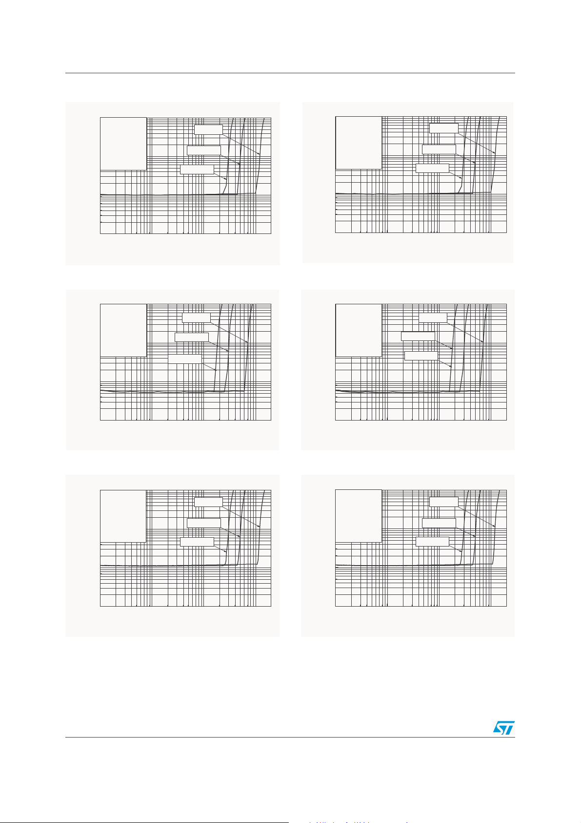
Figure 2. THD+N vs. output power Figure 3. THD+N vs. output power
10
RL = 8
Ω
G = 6dB
F = 20Hz
Cb = 1µF
BW < 125kHz
1
Tamb = 25°C
0.1
THD + N (%)
0.01
1E-3 0.01 0.1 1
Output power (W)
Vcc=5V
Vcc=3.3V
Vcc=2.6V
10
RL = 8
Ω
G = 6dB
F = 20Hz
Cb = 0
BW < 125kHz
1
Tamb = 25°C
0.1
THD + N (%)
0.01
1E-3 0.01 0.1 1
Output power (W)
Vcc=5V
Vcc=3.3V
Vcc=2.6V
Figure 4. THD+N vs. output power Figure 5. THD+N vs. output power
THD + N (%)
0.1
10
RL = 16
G = 6dB
F = 20Hz
Cb = 1µF
BW < 125kHz
1
Tamb = 25°C
Ω
Vcc=5V
Vcc=3.3V
Vcc=2.6V
10
THD + N (%)
0.1
RL = 16
G = 6dB
F = 20Hz
Cb = 0
BW < 125kHz
1
Tamb = 25°C
Ω
Vcc=5V
Vcc=3.3V
Vcc=2.6V
0.01
1E-3 0.01 0.1 1
Output power (W)
0.01
1E-3 0.01 0.1 1
Output power (W)
Figure 6. THD+N vs. output power Figure 7. THD+N vs. output power
10
RL = 8
Ω
G = 6dB
F = 1kHz
Cb = 1µF
BW < 125kHz
1
Tamb = 25°C
0.1
THD + N (%)
0.01
1E-3 0.01 0.1 1
Output power (W)
Vcc=5V
Vcc=3.3V
Vcc=2.6V
10
RL = 8
Ω
G = 6dB
F = 1kHz
Cb = 0
BW < 125kHz
1
Tamb = 25°C
0.1
THD + N (%)
0.01
1E-3 0.01 0.1 1
Output power (W)
Vcc=5V
Vcc=3.3V
Vcc=2.6V
8/24
 Loading...