

STMicroelectronics TS4990 Schematic [ru]
1W AUDIO POWER AMPLIFIER WITH ACTIVE LOW
■OPERATING FROM V
■1W OUTPUT POWER @ Vcc=5V, THD=1%,
f=1kHz, with 8
Ω Load
■ULTRA LOW CONSUMPTION IN STANDBY
MODE (10nA)
■62dB PSRR @ 217Hz @ Grounded mode
■Zero PO P & CLIC K
■ULTRA LOW DISTORTION (0.1%)
■UNITY GAIN STABLE
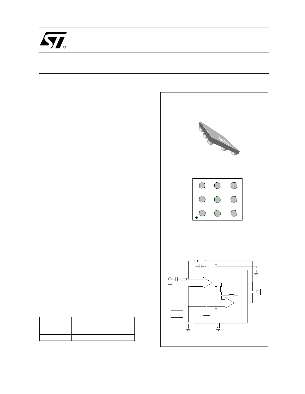
■AVAILABLE IN 9 BUMPS Flip Chip Package
= 2.2V to 5.5V
CC
STANDBY MODE
PIN CONNECTIONS (top view)
TS4990JT - FLIP CHIP
TS4990
ADVANCE DATA
DESCRIPTION
The TS4990 has been designed for demanding
audio applications such as m obile phones and t o
minimize the number of external components.
This Audio Power Amplifier is capable of delivering 1W of continuous RMS Ouput Powe r into an
Ω load @ 5V.
8
An externally controlle d standby m ode control re-
duces the supply current to less than 10nA. It also
includes an internal thermal shutdown protection.
The unity-gain stable amplifier can be configured
by external gain setting resistors.
APPLICATIONS
■Mobile Phones (Cellular / Cordless)
■Laptop / Notebook Computers
■PDAs
■Portable Audio Devices
ORDER CODE
Part Number
Temperature
Range
TS4990IJT -40, +85°C
Package
J
•
6
6
Vin-
Vin-
7
7
8
8
1
1
BYPASS VOUT2
BYPASS VOUT2
Vout1
Vout1
GNDGND VCC
GNDGND VCC
9
9
2
2
TYPICAL APPLICATION SCHEMATIC
Rfeed
Audio In
Cin
Standby
Control
Cfeed
Rin
7
Vin-
5
Vin+
1
Bypass
3
Standby
+
Cb
Vcc
48
VCCGND
-
+
-
AV = -1
+
Bias
9
Vin+
Vin+
STBY
STBY
Vout 1
Vout 2
TS4990
5
5
4
4
3
3
+
Cs
6
Speaker
8 Ohms
2
J = Flip Chip Package - only available in Tape & Reel (JT)
February 2003
This is a preliminary information on a new product now in development. Details are subject to change without notice.
1/6
TS4990
ABSOLUTE MAXIMUM RATINGS
Symbol Parameter Value Unit
V
T
T
R
Supply voltage
CC
V
Input Voltage
i
Operating Free Air Temperature Range -40 to + 85 °C
oper
Storage Temperature -65 to +150 °C
stg
T
Maximum Junction Temperature 150 °C
j
thja
Thermal Resistance Junction to Ambient
Flip Chip
Pd Power Dissipation Internally Limited
ESD Human Body Model 2 kV
ESD Machine Model 200 V
Latch-up Immunity Class A (200mA)
Lead Te mpera ture (solde ring, 10sec ) 250 °C
1. All voltages values are measured with respect to the ground pin.
2. The magnitude of input signal must never exceed V
3. Device is protected in case of over temperature by a thermal shutdown active @ 150°C.
OPERATING CONDITIONS
Symbol Parameter Value Unit
V
V
V
R
GND
T
R
Supply Voltage 2.2 to 5.5 V
CC
Common Mode Input Voltage Range
ICM
Standby Voltage Input :
STB
Device ON
Device OFF
R
Load Resistor 4 - 32
L
OUT
Resistor Output to GND > 1 M
Thermal Shutdown Temperature 150 min. °C
SD
thja
Thermal Resistance Junction to Ambient
1)
2)
3)
+ 0.3V / GND - 0.3V
CC
1.2 ≤ V
GND ≤ V
1)
6V
GND to V
CC
TBD
1.2V to V
STB
STB
CC
≤ V
≤ 0.4
CC
TBD °C/W
V
°C/W
V
V
Ω
Ω
1. This thermal resistance can be reduced with a suitable PCB layout .
2/6
TS4990
ELECTRICAL CHARACTERISTICS
V
= +5V, GND = 0V , T
CC
Symbol Parameter Min. Typ. Max. Unit
= 25°C (unless otherwise specified)
amb
I
CC
I
STANDBY
Voo
Po
THD + N
PSRR
T
WU
1. Standby mode is actived wh en Vstdby is tied to Gnd
2. Dynamic mea surements - 20*log(rms(Vout )/ rms(Vri ppl e)). Vripple is the suri mposed s i nus signal to Vc c.
= +3.3V, GND = 0V, T
V
CC
Supply Current
No input signal, no load 4 6
Standby Current
No input signal, Vstdby = GND, RL = 8
1)
Ω
10 1000 nA
Output Offset Voltage
No input signal, RL = 8
Ω
Output Power
THD = 1% Max, f = 1kHz, RL = 8
Ω
Total Harmonic Distortion + Noise
Po = 250mW rms, Gv = 2, 20Hz < f < 20kHz, RL = 8
Power Supply Rejection Ratio
RL = 8
Gv = 2, Vripple = 200mVpp, Input Grounded
Ω,
2)
F = 217Hz
F = 1kHz
0.8 1 W
Ω
55
55
520
0.15 %
62
66
Wake-Up Time 100 TBD ms
= 25°C (unless otherwise specified)
amb
Symbol Parameter Min. Typ. Max. Unit
I
CC
I
STANDBY
Supply Current
No input signal, no load 4 6
Standby Current
No input signal, Vstdby = GND, RL = 8
1)
Ω
10 1000 nA
mA
mV
dB
mA
Voo
Po
THD + N
PSRR
T
WU
1. Standby mode i s actived when Vstdby is tied to Vcc
2. Dynamic mea surements - 20*log(rms(Vout )/ rms(Vri ppl e)). Vripple is the suri mposed s i nus signal to Vc c.
Output Offset Voltage
No input signal, RL = 8
Output Power
THD = 1% Max, f = 1kHz, RL = 8
Ω
Ω
380 450 mW
Total Harmonic Distortion + Noise
Po = 250mW rms, Gv = 2, 20Hz < f < 20kHz, RL = 8
Power Supply Rejection Ratio
RL = 8
Gv = 2, Vripple = 200mVpp, Input Grounded
Ω,
2)
F = 217Hz
F = 1kHz
Ω
55
55
Wake-Up Time 130 TBD ms
520
mV
0.15 %
62
dB
66
3/6
 Loading...