

Page 1

Low Power Single Operational Amplifier
■ Offset null capability (by external
compensation)
■ Dynamic characteristics adjustable I
■ Consumption current and dynamic
parameters are stable regarding the
voltage power supply variations
■ Output voltage can swing to ground
■ Very large I
■ Stable and low offset voltage
■ Three input offset voltage selections
SET
range
TS271
CMOS Programmable
SET
N
DIP8
(Plastic Package)
Description
The TS271 is a low cost, low power single
operational amplifier designed to operate with
(Plastic Micropackage)
D
SO-8
single or dual supplies. This operational amplifier
uses the ST silicon gate CMOS process giving it
an excellent consumption-speed ratio. This
Pin Connections (top view)
amplifier is ideally suited for low consumption
applications.
The power supply is externally programmable with
a resistor connected between pins 8 and 4. It
allows to choose the best consumption-speed
ratio and supply current can be minimized
according to the required speed. This device is
specified for the following I
current values:
SET
1.5µA, 25µA, 130µA.
This CMOS amplifier offers very high input
impedance and extremely low input currents. The
major advantage versus JFET devices is the very
low input currents drift with temperature see
1
2
3
45
-
+
1 - Offset Null 1
2 - Inverting Input 1
3 - Non-inverting Input 1
-
4 - V
CC
5 - Offset Null 2
6 - Output
+
7 - V
CC
8 - I
Set
8
7
6
Figure 8, Figure 19, Figure 30.
Order Codes
Part Number Temperature Range Package Packaging
TS271CN/ACN
TS271CD/CDT/ACD/ACDT SO Tube and Tape & Reel
TS271IN/AIN/
TS271ID/IDT/AID/AIDT/BID/BIDT SO Tube and Tape & Reel
TS271BMD -55°C, +125°C SO Tube
0°C, +70°C
-40°C, +125°C
DIP Tube
DIP Tube
March 2005 Revision 2 1/17
Page 2

TS271 Block Diagram
1 Block Diagram
Figure 1. Application block diagram
2/17
Page 3

Absolute Maximum Ratings TS271
2 Absolute Maximum Ratings
Table 1. Key parameters and their absolute maximum ratings
Symbol Parameter TS271C/AC/BC TS271I/AI/BI TS271M/AM/BM Unit
+
VCC
Vid
T
T
1) All values, except differential voltage are with respect to network ground terminal.
2) Differential voltages are the non-inverting input terminal with respect to the inverting input terminal.
3) The magnitude of the input and the output voltages must never exceed the magnitude of the positive supply voltage.
Supply Voltage
Differential Input Voltage
V
Input Voltage
i
I
Output Current for V
o
I
Input Current
in
Operating Free-Air Temperature Range
oper
Storage Temperature Range
stg
Table 2. Operating conditions
Symbol Parameter Value Unit
+
V
V
Supply Voltage
CC
Common Mode Input Voltage Range
icm
1
2
3
+
≥ 15V
CC
18 V
±18 V
-0.3 to 18 V
±30 mA
±5 mA
0 to +70 -40 to +125 -55 to +125 °C
-65 to +150 °C
3 to 16 V
0 to V
CC
+
- 1.5
V
3/17
Page 4

TS271 Absolute Maximum Ratings
Figure 2. Schematic Diagram
4/17
Page 5

Absolute Maximum Ratings TS271
Figure 3. Offset voltage null circuit
-
5
1
+
8
25kΩ
R
set
OFFSET COMPENSATION GUARANTEED FOR
TS271BCX (I > 25 A), TS271ACX (I > 90 A)
SET SETµµ
Figure 4. Offset voltage null circuit
-
5
1
+
8
25kΩ
Figure 5. Resistor biasing
+
V
CC
-
-
V
CC
+
-
V
CC
CONNECTED TO GROUND
R
set
V
O
R
set
CONNECTED TO
R
set
+
V
CC
-
V
O
+
R
set
-
V
CC
-
VALUE :SEE Fig. 1)
(R
V
set
CC
Figure 6. Rset connected to Vcc-
V = +3VCC
V = +5VCC
Rset
-
V
CC
10MΩ
V = +16VCC
V = +10VCC
R
set
OFFSET COMPENSATION GUARANTEED FOR
TS271BCX (I > 25 A), TS271ACX (I > 90 A)
SET SETµµ
1MΩ
100kΩ
10kΩ
0.1 Aµ 1Aµ 10 Aµ 100 Aµ
I
set
5/17
Page 6

TS271 Electrical Characteristics
3 Electrical Characteristics
Table 3. for I
= 1.5µA - V
SET
CC
+
Symbol Parameter
Input Offset Voltage
V
= 1.4V, Vic = 0V TS271C/I/M
O
V
DV
io
Input Offset Voltage Drift
io
Input Offset Current note
I
io
≤ T
T
min
amb
≤ T
Vic = 5V, VO = 5V
≤ T
T
min
amb
≤ T
max
1
max
Input Bias Current - see note 1
I
ib
Vic = 5V, VO = 5V
≤ T
T
min
amb
≤ T
max
High Level Output Voltage
= 100mV, RL = 1MΩ
V
OH
V
OL
V
id
T
≤ T
amb
≤ T
max
min
Low Level Output Voltage
= -100mV
V
id
Large Signal Voltage Gain
V
A
vd
GBP
CMR
SVR
Gain Bandwidth Product
Common Mode Rejection Ratio
Supply Voltage Rejection Ratio
= 5V, RL = 1MΩ, Vo = 1V to 6V
iC
= 40dB, RL = 1MΩ, CL = 100pF, fin = 100kHz
A
v
V
= 1V to 7.4V, Vo = 1.4V
iC
+
V
= 5V to 10V, Vo = 1.4V
CC
Supply Current (per amplifier)
A
I
I
sink
SR
CC
I
o
= 1, no load, Vo = 5V
v
≤ T
T
min
amb
≤ T
max
Output Short Circuit Current
V
= 0V, Vid = 100mV
o
Output Sink Current
V
= VCC, Vid = -100mV
o
Slew Rate at Unity Gain
R
= 1MΩ, CL = 100pF, Vi = 3 to 7V
L
Phase Margin at Unity Gain
A
φm
= 40dB, RL = 1MΩ CL = 10pF
v
Overshoot Factor
A
K
OV
e
n
= 40dB, RL = 1MΩ CL = 10pF
v
Equivalent Input Noise Voltage
f = 1kHz, R
= 100Ω
s
= +10V, V
TS271AC/AI/AM
TS271BC/BI/BM
TS271C/I/M
TS271AC/AI/AM
TS271BC/BI/BM
≤ T
T
min
= 100pF
C
L
= 100pF
C
L
CC
-
amb
= 0V, T
≤ T
max
= +25°C (unless otherwise specified)
amb
TS271C/AC/BC
TS271I/AI/BI
TS271M/AM/BM
Min. Typ. Max. Min. Typ. Max.
1.1
0.9
0.25
10
5
2
12
1.1
0.9
0.25
6.5
3
22µV/°C
8.8
8.7
1
100
1
150
98.8
8.6
1
200
1
300
9V
50 50
3020100 3020100 V/mV
0.1 0.1
60 80 60 80
60 80 60 80
10 15
10 15
17
60 60
45 45
0.04 0.04
35
10
40
70
35
10
40
70
30 30
10
5
2
12
6.5
3.5
18
Unit
mV
pA
pA
mV
MHz
dB
dB
µA
mA
mA
V/
µs
Degrees
%
nV
-----------Hz
1) Maximum values including unavoidable inaccuracies of the industrial test.
6/17
Page 7
Electrical Characteristics TS271
6
Typical characteristics for I
= 1 .5 µA
SET
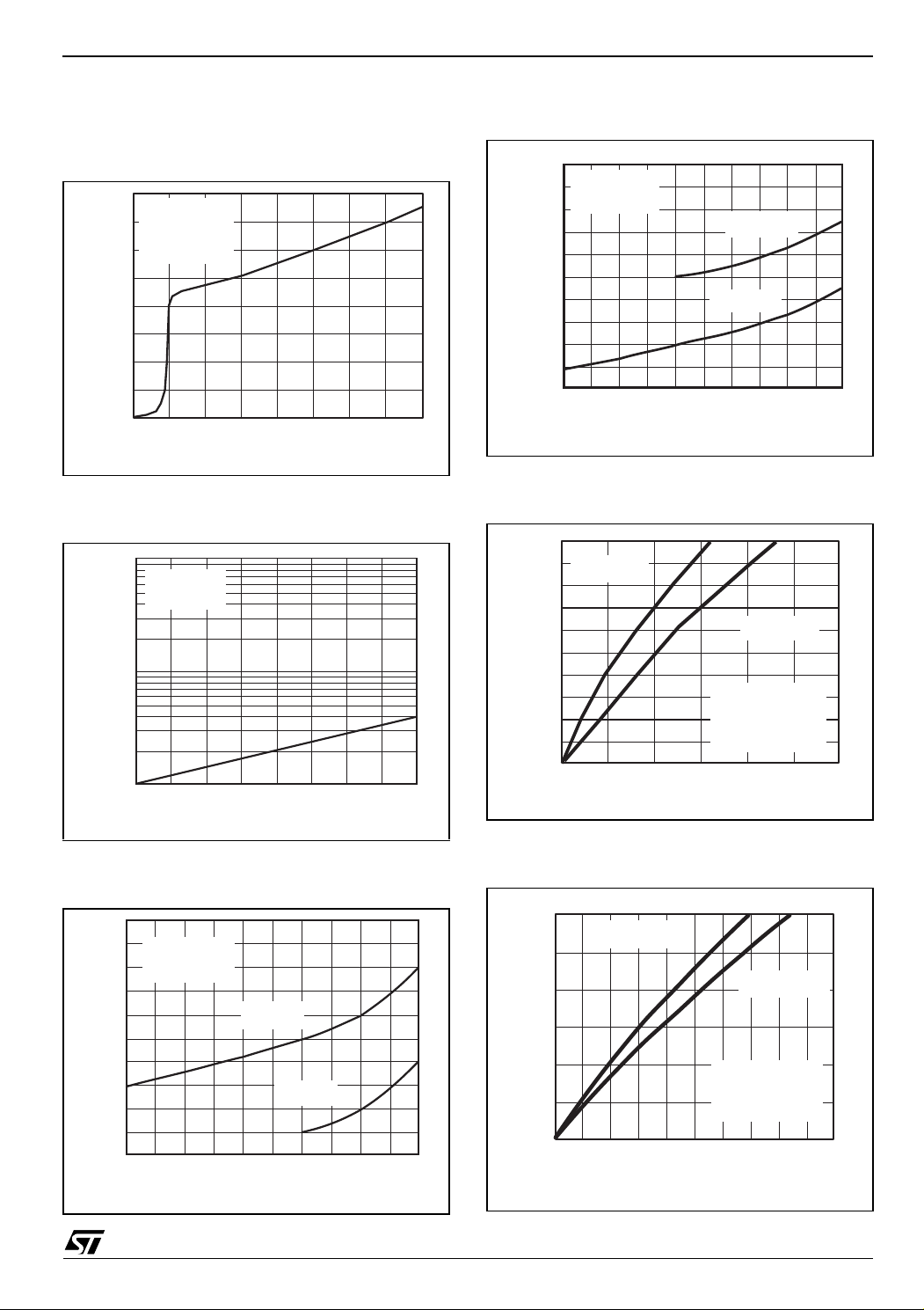
Figure 7. Supply current versus supply
voltage
20
)
A
µ
15
CC
T=25C
amb
A=1
V
V=V /2
OCC
°
10
5
SUPPLY CURRENT, I (
0
48121
SUPPLY VOLTAGE, V (V)
CC
Figure 8. Input bias current versus free air
temperature
100
V = 10V
CC
V = 5V
IB
i
Figure 10. High level output voltage versus
high level output current
20
T = 25 C
V = 100mV
16
H
O
12
8
4
OUTPUT VOLTAGE, V (V)
0
-50 -40 -30 -20 -10 0
°
amb
id
V = 10V
CC
OUTPUT CURRENT, I (mA)
V = 16V
CC
OH
Figure 11. Low level output voltage versus low
level output current
1.0
V
=3V
OL
0.8
0.6
CC
V=5V
CC
10
INPUT BIAS CURRENT, I (pA)
1
25 50 75 100 125
TEMPERATURE, T ( °C)
amb
Figure 9. High level output voltage versus
high level output current
5
T = 25 C
amb
4
V = 100mV
OH
id
3
2
1
OUTPUT VOLTAGE, V (V)
0
-10 -8 -6 -4 -2 0
°
V = 5V
CC
V=3V
CC
OUTPUT CURRENT, I (mA)
OH
0.4
T=25°C
0.2
amb
V = 0.5V
ic
V = -100mV
id
OUTPUT VOLTAGE, V (V)
0123
OUTPUT CURRENT, I (mA)
OL
Figure 12. Low level output voltage versus low
level output current
3
(V)
OL
2
1
OUTPUT VOLTAGE, V
0 4 8121620
V=10V
CC
V=16V
CC
T = 25°C
amb
V=0.5V
i
V = -100mV
id
OUTPUT CURRENT, I (mA)
OL
7/17
Page 8
TS271 Electrical Characteristics
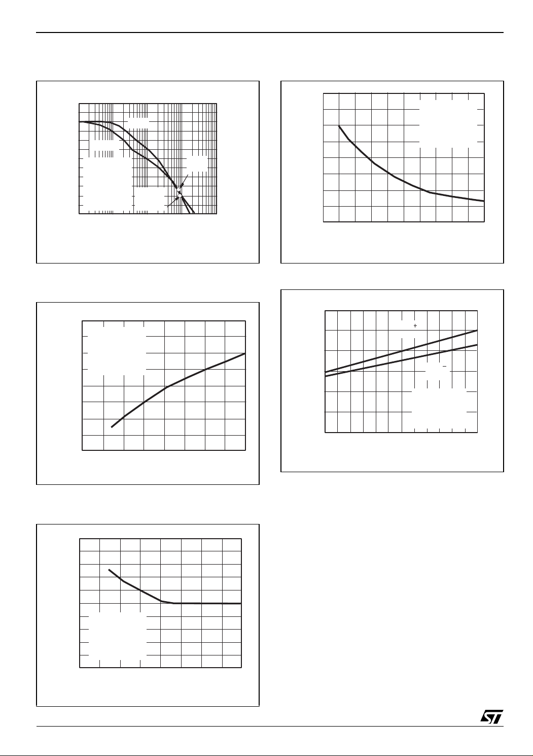
Figure 13. Open loop frequency response and
phase shift
50
40
30
20
10
GAIN (dB)
0
-10
10
PHASE
T = 25°C
amb
V=10V
CC
R=
L
C = 100pF
L
A=100
VCL
23
GAIN
+
1M
Ω
Gai n
Bandwidth
Product
10
4
10
FREQUENCY, f (Hz)
10
0
45
Phase
Mar gin
5
10
90
135
PHASE (Degrees)
180
6
Figure 14. Gain bandwidth product versus
supply voltage
120
T
= 25°C
amb
Ω
R=1M
100
80
60
40
GAIN BANDW. PROD., GBP (MHz)
L
C = 100pF
L
A
=1
V
0
4 8 12 16
SUPPLY VOLTAGE, V
CC
(V)
Figure 16. Phase margin versus capacitive
load
40
T
= 25°C
amb
L
V
CC
Ω
=1
30
(Degrees)
m
φ
R=1M
A
V=10V
20
10
PHASE MARGIN,
0
20
6040
CAPACITANCE, C
L
80
(pF)
100
Figure 17. Slew rate versus supply voltage
0.07
s)
0.06
µ
,
0.05
SR (V/
0.04
0.03
0.02
SLEW RATES
0.01
4 6 8 10 12 14 16
SUPPLY VOLTAGE, V (V)
SR
T
R=
C = 100pF
amb
L
L
SR
= 25°C
1M
CC
Ω
Figure 15. Phase margin versus supply
voltage
10
8
6
φ
4
T
= 25°C
amb
R=1M
Ω
L
C = 100pF
L
A
=1
V
48
SUPPLY VOLTAGE, V (V)
12
CC
8/17
2
PHASE MARGIN, m (Degrees)
0
16
Page 9

Electrical Characteristics TS271
4 Electrical Characteristics
Table 4. for I
= 25µA - V
SET
+
= +10V, V
CC
Symbol Parameter
Input Offset Voltage
V
= 1.4V, Vic = 0V TS271C/I/M
O
V
DV
io
Input Offset Voltage Drift
io
Input Offset Current note
I
io
≤ T
T
min
amb
≤ T
Vic = 5V, VO = 5V
≤ T
T
min
amb
≤ T
max
1
max
Input Bias Current - see note 1
I
ib
Vic = 5V, VO = 5V
≤ T
T
min
amb
≤ T
max
High Level Output Voltage
= 100mV, RL = 100kΩ
V
OH
V
OL
V
id
T
≤ T
amb
≤ T
max
min
Low Level Output Voltage
= -100mV
V
id
Large Signal Voltage Gain
V
A
vd
GBP
CMR
SVR
Gain Bandwidth Product
Common Mode Rejection Ratio
Supply Voltage Rejection Ratio
= 5V, RL = 100kΩ, Vo = 1V to 6V
iC
= 40dB, RL = 100kΩ, CL = 100pF, fin = 100kHz
A
v
V
= 1V to 7.4V, Vo = 1.4V
iC
+
V
= 5V to 10V, Vo = 1.4V
CC
Supply Current (per amplifier)
A
I
I
sink
SR
CC
I
o
= 1, no load, Vo = 5V
v
≤ T
T
min
amb
≤ T
max
Output Short Circuit Current
V
= 0V, Vid = 100mV
o
Output Sink Current
V
= VCC, Vid = -100mV
o
Slew Rate at Unity Gain
R
= 100kΩ, CL = 100pF, Vi = 3 to 7V
L
Phase Margin at Unity Gain
A
φm
= 40dB, RL = 100kΩ CL = 10pF
v
Overshoot Factor
A
K
OV
e
n
= 40dB, RL = 100kΩ CL = 10pF
v
Equivalent Input Noise Voltage
f = 1kHz, R
= 100Ω
s
-
= 0V, T
CC
TS271AC/AI/AM
TS271BC/BI/BM
TS271B/C/I/M
TS271AC/AI/AM
TS271BC/BI/BM
≤ T
T
min
= 100pF
C
L
= 100pF
C
L
amb
≤ T
= +25°C (unless otherwise specified)
amb
TS271C/AC/BC
TS271I/AI/BI
TS271M/AM/BM
Min. Typ. Max. Min. Typ. Max.
1.1
0.9
0.25
10
5
2
12
1.1
0.9
0.25
6.5
3
22µV/°C
1
1
100
1
1
150
8.7
8.9 8.7
8.6
8.9 V
8.5
50 50
302050 301050 V/mV
max
0.7 0.7
60 80 60 80
60 80 60 80
150 200
150 200
250
60 60
45 45
0.6 0.6
50
30
30
50
50
30
30
50
38 38
10
5
2
12
6.5
3.5
200
300
300
Unit
mV
pA
pA
mV
MHz
dB
dB
µA
mA
mA
V/
µs
Degrees
%
nV
-----------Hz
1) Maximum values including unavoidable inaccuracies of the industrial test.
9/17
Page 10
TS271 Electrical Characteristics
Typical characteristics for I
= 25 µA
SET
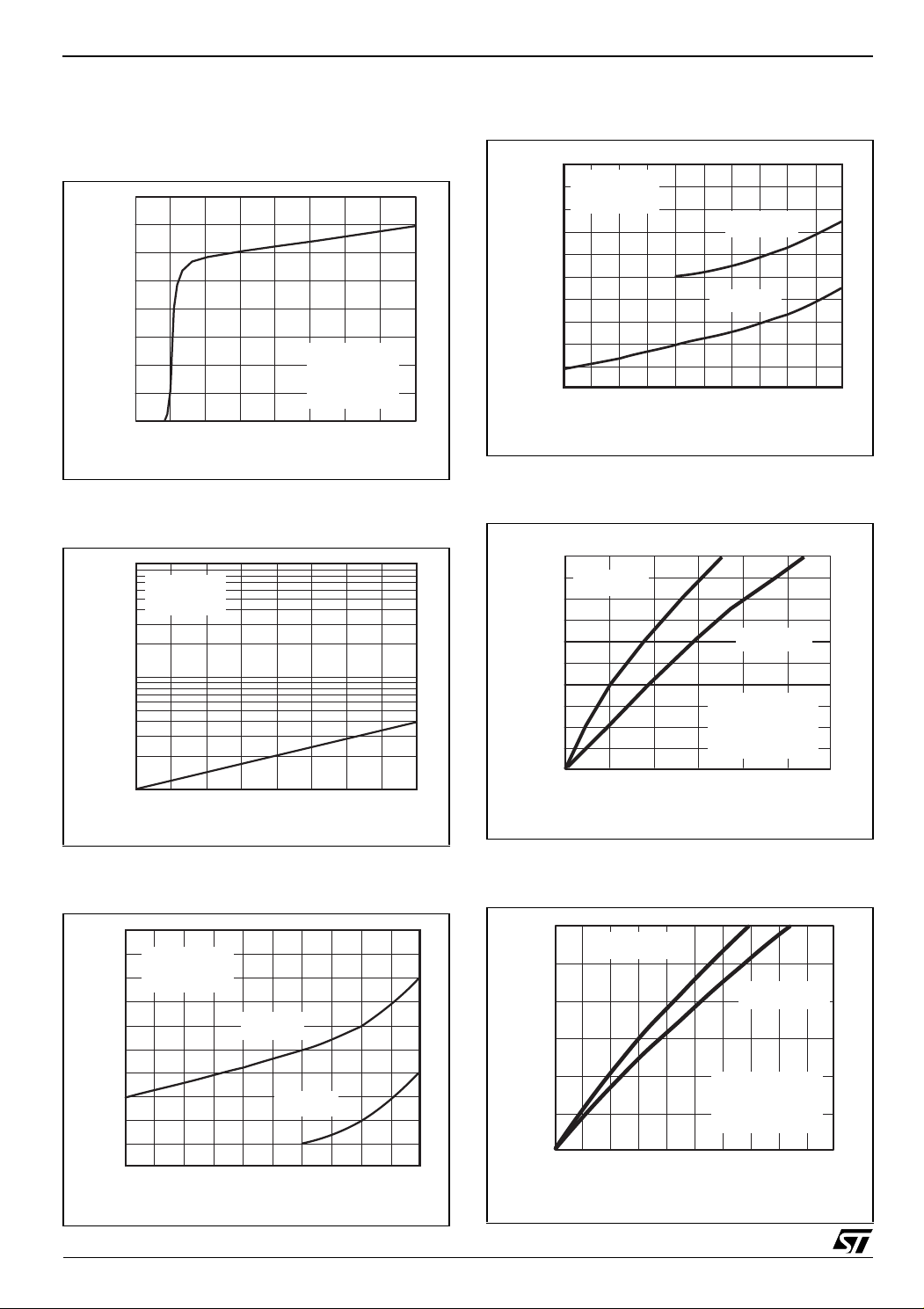
Figure 18. Supply current versus supply
voltage
200
)
A
µ
150
CC
100
T=25C
50
SUPPLY CURRENT, I (
0
4 8 12 16
amb
A=1
V
V=V /2
OCC
SUPPLY VOLTAGE, V (V)
°
CC
Figure 19. Input bias current versus free air
temperature
100
V = 10V
CC
V = 5V
IB
i
Figure 21. High level output voltage versus
high level output current
20
T = 25 C
V = 100mV
16
H
O
12
8
4
OUTPUT VOLTAGE, V (V)
0
-50 -40 -30 -20 -10 0
°
amb
id
V = 10V
CC
OUTPUT CURRENT, I (mA)
V = 16V
CC
OH
Figure 22. Low level output voltage versus low
level output current
1.0
V
=3V
OL
0.8
0.6
CC
V=5V
CC
10
INPUT BIAS CURRENT, I (pA)
1
25 50 75 100 125
TEMPERATURE, T ( °C)
amb
Figure 20. High level output voltage versus
high level output current
5
T = 25 C
amb
4
V = 100mV
OH
id
3
2
1
OUTPUT VOLTAGE, V (V)
0
-10 -8 -6 -4 -2 0
°
V = 5V
CC
V=3V
CC
OUTPUT CURRENT, I (mA)
OH
0.4
T=25°C
0.2
OUTPUT VOLTAGE, V (V)
0123
OUTPUT CURRENT, I (mA)
amb
V = 0.5V
ic
V = -100mV
id
OL
Figure 23. Low level output voltage versus low
level output current
3
(V)
OL
2
1
OUTPUT VOLTAGE, V
0 4 8121620
V=10V
CC
V=16V
CC
T = 25°C
amb
V=0.5V
i
V = -100mV
id
OUTPUT CURRENT, I (mA)
OL
10/17
Page 11
Electrical Characteristics TS271
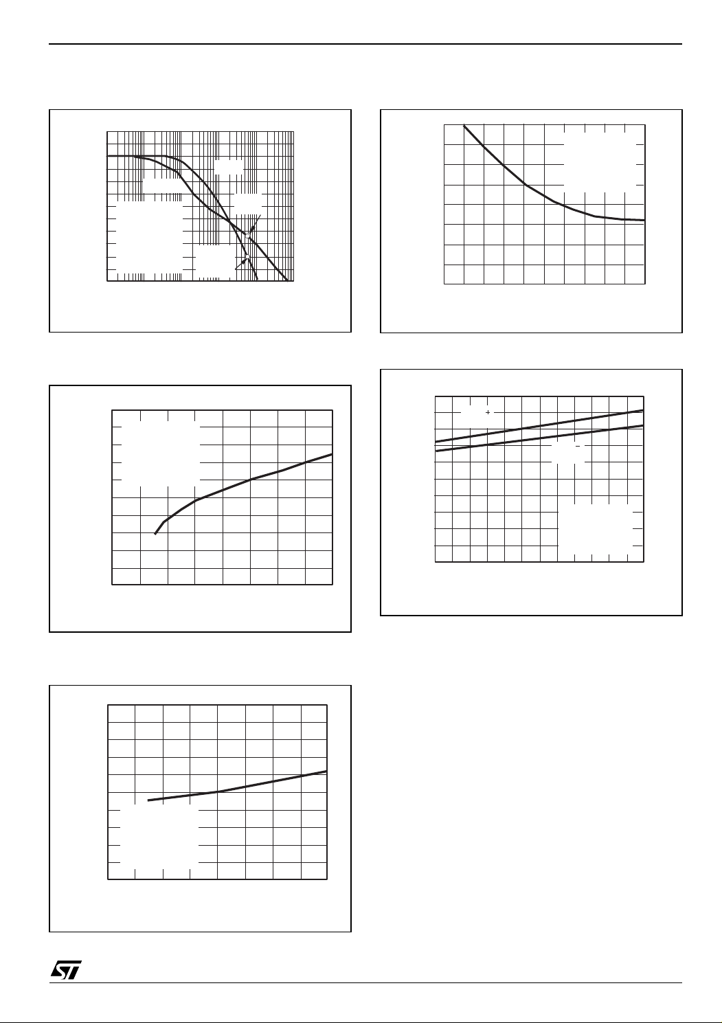
Figure 24. Open loop frequency response and
phase shift
50
40
30
20
10
GAIN (dB)
0
-10
10
PHASE
T = 25°C
amb
+
V=10V
CC
R=
100k
Ω
L
C = 100pF
L
A=100
VCL
23
10
10
FREQUENCY, f (Hz)
Gai n
Bandwidth
Product
4
GAIN
5
10
Phase
Mar gin
10
0
45
90
135
PHASE (Degrees)
180
7
6
10
Figure 25. Gain bandwidth product versus
supply voltage
0.9
T
= 25°C
0.8
0.7
0.6
0.5
0.4
GAIN BANDW. PROD., GBP (MHz)
amb
R = 100k
L
C = 100pF
L
A
V
0
Ω
=1
4 8 12 16
SUPPLY VOLTAGE, V
CC
(V)
Figure 27. Phase margin versus capacitive
load
50
T
= 25°C
amb
L
V
CC
Ω
=1
40
(Degrees)
m
φ
R = 100k
A
V=10V
30
20
PHASE MARGIN,
0
20
6040
CAPACITANCE, C
L
80
(pF)
100
Figure 28. Slew rate versus supply voltage
1.0
s)
µ
0.8
0.6
0.4
0.2
SLEW RATES, SR (V/
0
SR
SR
T
= 25°C
amb
R = 100k
C = 100pF
Ω
L
L
4 6 8 10 12 14 16
SUPPLY VOLTAGE, V (V)
CC
Figure 26. Phase margin versus supply
voltage
50
40
30
φ
20
T
= 25°C
amb
R = 100k
10
C = 100pF
A
PHASE MARGIN, m (Degrees)
0
Ω
L
L
=1
V
48
SUPPLY VOLTAGE, V (V)
12
CC
16
11/17
Page 12

TS271 Electrical Characteristics
5 Electrical Characteristics
Table 5 . for I
= 130µA - V
SET
CC
+
Symbol Parameter
Input Offset Voltage
V
= 1.4V, Vic = 0V TS271C/I/M
O
V
DV
io
Input Offset Voltage Drift
io
Input Offset Current note
I
io
≤ T
T
min
amb
≤ T
Vic = 5V, VO = 5V
≤ T
T
min
amb
≤ T
max
1
max
Input Bias Current - see note 1
I
ib
Vic = 5V, VO = 5V
≤ T
T
min
amb
≤ T
max
High Level Output Voltage
= 100mV, RL = 10kΩ
V
OH
V
OL
V
id
T
≤ T
amb
≤ T
max
min
Low Level Output Voltage
= -100mV
V
id
Large Signal Voltage Gain
V
A
vd
GBP
CMR
SVR
Gain Bandwidth Product
Common Mode Rejection Ratio
Supply Voltage Rejection Ratio
= 5V, RL = 10kΩ, Vo = 1V to 6V
iC
= 40dB, RL = 10kΩ, CL = 100pF, fin = 100kHz
A
v
V
= 1V to 7.4V, Vo = 1.4V
iC
+
V
= 5V to 10V, Vo = 1.4V
CC
Supply Current (per amplifier)
A
I
I
sink
SR
CC
I
o
= 1, no load, Vo = 5V
v
≤ T
T
min
amb
≤ T
max
Output Short Circuit Current
V
= 0V, Vid = 100mV
o
Output Sink Current
V
= VCC, Vid = -100mV
o
Slew Rate at Unity Gain
R
= 10kΩ, CL = 100pF, Vi = 3 to 7V
L
Phase Margin at Unity Gain
A
φm
= 40dB, RL = 10kΩ CL = 10pF
v
Overshoot Factor
A
K
OV
e
n
= 40dB, RL = 10kΩ CL = 10pF
v
Equivalent Input Noise Voltage
f = 1kHz, R
= 100Ω
s
= +10V, V
TS271AC/AI/AM
TS271BC/BI/BM
TS271B/C/I/M
TS271AC/AI/AM
TS271BC/BI/BM
≤ T
T
min
= 100pF
C
L
= 100pF
C
L
-
= 0V, T
CC
amb
≤ T
= +25°C (unless otherwise specified)
amb
TS271C/AC/BC
TS271I/AI/BI
TS271M/AM/BM
Min. Typ. Max. Min. Typ. Max.
1.1
0.9
0.25
10
5
2
12
1.1
0.9
0.25
6.5
3
22µV/°C
1
100
1
150
8.2
8.4 8.288.4 V
8.1
50 50
10715 10615 V/mV
max
2.3 2.3
60 80 60 80
60 70 60 70
800 1300
800 1300
1400
60 60
45 45
4.5 4.5
65
30
30
50
65
30
30
50
30 30
Unit
10
5
2
mV
12
6.5
3.5
1
pA
200
1
pA
300
mV
MHz
dB
dB
µA
1500
mA
mA
V/
µs
Degrees
%
nV
-----------Hz
1) Maximum values including unavoidable inaccuracies of the industrial test.
12/17
Page 13

Electrical Characteristics TS271
Typical characteristics for I
= 130µA
SET
Figure 29. Supply current (each amplifier)
versus supply voltage
1.0
)
A
m
0.8
CC
0.6
0.4
T=25C
0.2
SUPPLY CURRENT, I (
0
4
8
SUPPLY VOLTAGE, V (V)
amb
A=1
V=V /2
OCC
CC
°
V
12 1
Figure 30. Input bias current versus free air
temperature
100
V = 10V
CC
V = 5V
IB
i
Figure 32. High level output voltage versus
high level output current
20
T = 25 C
V = 100mV
16
H
O
12
8
4
OUTPUT VOLTAGE, V (V)
0
-50 -40 -30 -20 -10 0
6
°
amb
id
V = 10V
CC
OUTPUT CURRENT, I (mA)
V = 16V
CC
OH
Figure 33. Low level output voltage versus low
level output current
1.0
V
=3V
OL
0.8
0.6
CC
V=5V
CC
10
INPUT BIAS CURRENT, I (pA)
1
25 50 75 100 125
TEMPERATURE, T ( °C)
amb
Figure 31. High level output voltage versus
high level output current
5
T = 25 C
amb
4
V = 100mV
OH
3
2
1
OUTPUT VOLTAGE, V (V)
0
-10 -8 -6 -4 -2 0
°
id
V = 5V
CC
V=3V
CC
OUTPUT CURRENT, I (mA)
OH
0.4
T=25°C
0.2
OUTPUT VOLTAGE, V (V)
0123
OUTPUT CURRENT, I (mA)
amb
V = 0.5V
ic
V = -100mV
id
OL
Figure 34. Low level output voltage versus low
level output current
3
(V)
OL
2
1
OUTPUT VOLTAGE, V
0 4 8121620
V=10V
CC
V=16V
CC
T = 25°C
amb
V=0.5V
i
V = -100mV
id
OUTPUT CURRENT, I (mA)
OL
13/17
Page 14

TS271 Electrical Characteristics
Figure 35. Open loop frequency response and
phase shift
50
40
30
20
10
GAIN (dB)
0
-10
10
PHASE
T = 25°C
amb
+
V=10V
CC
R = 10k
C = 100pF
A=100
23
Ω
L
L
VCL
10
10
FREQUENCY, f (Hz)
GAIN
Phase
Mar gin
Gai n
Bandwidth
Product
4
5
10
10
0
45
90
135
PHASE (Degrees)
180
7
6
10
Figure 36. Gain bandwidth product versus
supply voltage
5
T
= 25°C
amb
4
R = 10k
C = 100pF
3
A
2
1
0
GAIN BANDW. PROD., GBP (MHz)
Ω
L
L
=1
V
4 8 12 16
SUPPLY VOLTAGE, V
CC
(V)
Figure 38. Phase margin versus capacitive
load
70
T
= 25°C
amb
L
V
CC
Ω
=1
(Degrees)
m
φ
A
V=10V
60
R = 10k
50
40
30
PHASE MARGIN,
200
6040
CAPACITANCE, C
L
(pF)
80
100
Figure 39. Slew rate versus supply voltage
5
s)
µ
SLEW RATES, SR (V/
SR
4
3
SR
2
T
= 25°C
amb
1
R = 10k
C = 100pF
0
4 6 8 10 12 14 16
SUPPLY VOLTAGE, V (V)
Ω
L
L
CC
Figure 37. Phase margin versus supply
voltage
50
40
30
φ
20
T
= 25°C
amb
Ω
L
L
=1
V
48
SUPPLY VOLTAGE, V (V)
12
CC
14/17
R = 10k
10
C = 100pF
A
PHASE MARGIN, m (Degrees)
0
16
Page 15
Package Mechanical Data TS271
6 Package Mechanical Data
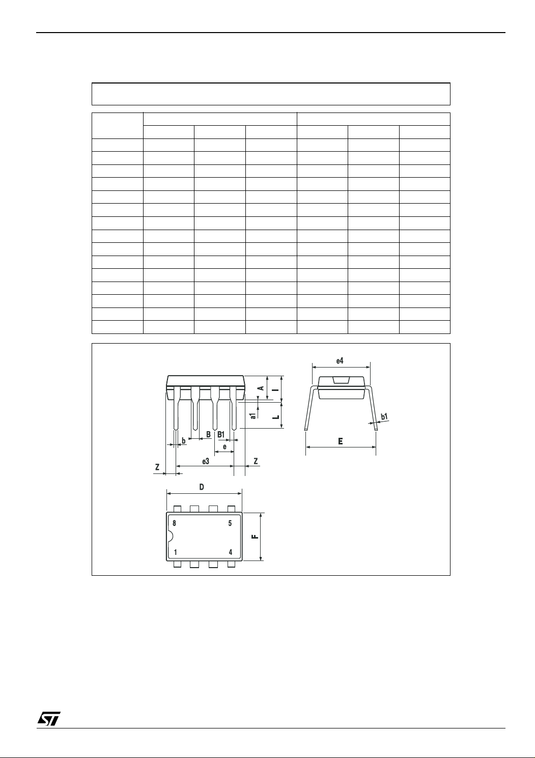
Plastic DIP-8 MECHANICAL DATA
DIM.
A 3.3 0.130
a1 0.7 0.028
B 1.39 1.65 0.055 0.065
B1 0.91 1.04 0.036 0.041
b 0.5 0.020
b1 0.38 0.5 0.015 0.020
D 9.8 0.386
E 8.8 0.346
e 2.54 0.100
e3 7.62 0.300
e4 7.62 0.300
F 7.1 0.280
I 4.8 0.189
L 3.3 0.130
Z 0.44 1.6 0.017 0.063
MIN. TYP MAX. MIN. TYP. MAX.
mm. inch
P001F
15/17
Page 16

TS271 Package Mechanical Data
Package Mechanical Data
SO-8 MECHANICAL DATA
DIM.
A 1.35 1.75 0.053 0.069
A1 0.10 0.25 0.04 0.010
A2 1.10 1.65 0.043 0.065
B 0.33 0.51 0.013 0.020
C 0.19 0.25 0.007 0.010
D 4.80 5.00 0.189 0.197
E 3.80 4.00 0.150 0.157
e 1.27 0.050
H 5.80 6.20 0.228 0.244
h 0.25 0.50 0.010 0.020
L 0.40 1.27 0.016 0.050
k ˚ (max.)
ddd 0.1 0.04
MIN. TYP MAX. MIN. TYP. MAX.
mm. inch
8
16/17
0016023/C
Page 17

Revision History TS271
7 Revision History
Date Revision Description of Changes
01 Nov. 2001 1 First Release
01 March 2005 2
• Application block diagram updated on Figure 2 on page 4
• Schematic Diagram updated on Figure 4 on page 5
Information furnished is believed to be accurate and reliable. However, STMicroelectronics assumes no responsibility for the consequences
of use of such information nor for any infringement of patents or other rights of third parties which may result from its use. No license is granted
by implication or otherwise under any patent or patent rights of STMicroelectronics. Specifications mentioned in this publication are subject
to change without notice. This publication supersedes and replaces all information previously supplied. STMicroelectronics products are not
authorized for use as critical components in life support devices or systems without express written approval of STMicroelectronics.
The ST logo is a registered trademark of STMicroelectronics
All other names are the property of their respective owners
© 2005 STMicroelectronics - All rights reserved
Australia - Belgium - Brazil - Canada - China - Czech Republic - Finland - France - Germany - Hong Kong - India - Israel - Italy - Japan -
Malaysia - Malta - Morocco - Singapore - Spain - Sweden - Switzerland - United Kingdom - United States of America
STMicroelectronics group of companies
www.st.com
17/17
 Loading...