

Page 1
■ Adjustable output voltage: 2.5 to 36V
■ Sink current capability: 1 to 100mA
■ Typical output impedance: 0.22Ω
■ 1% and 2% voltage precision
Description
The TL431 is a programmable shunt voltage
reference with guaranteed temperature stability
over the entire temperature range of operation.
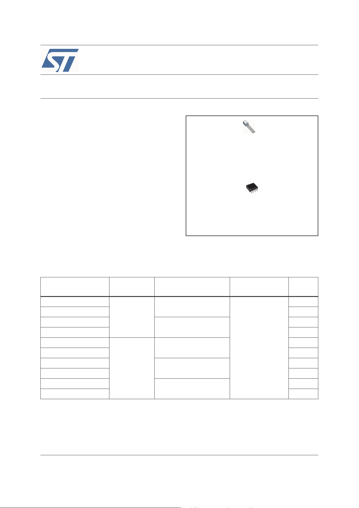
TL431
Programmable Voltage Reference
Z
TO92
(Plastic Package)
The output voltage may be set to any value
between 2.5V and 36V with two external resistors.
The TL431 operates with a wide current range
(Plastic Micropackage)
D
SO-8
from 1 to 100mA with a typical dynamic
impedance of 0.22Ω.
Order Codes
Part Number
TL431CD/CDT
TL431ACD/ACDT 431AC
TL431CZ/CZT/CZ-AP
TL431ACZ/ACZT/ACZ-AP TL431AC
TL431ID/IDT
TL431AID/AIDT 431AI
TL431IZ/IZT/IZ-AP
TL431AIZ/AIZT/AIZ-AP TL431AI
Temperature
Range
0, +70°C
-40, + 105°C
Package Packing Marking
SO-8
TO92
SO-8
TO92
Tube or Tape & Reel
431C
TL431C
431I
TL431I
TL431IYD/IYDT
SO-8 (automotive grade level)
TL431AIYD/AIYDT 431AIY
November 2005 1/13
431IY
Rev 2
www.st.com
13
Page 2
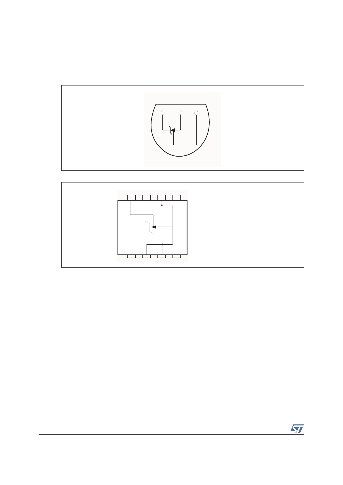
Pin Diagrams TL431
1 Pin Diagrams
Figure 1. TO92 pin connections (top view)
Cathode
Anode
123
Figure 2. SO-8 pin connections (top view)
8765
1234
Reference
1 - Cathode
2 - Anode
3 - Anode
4 - N.C.
5 - N.C.
6 - Anode
7 - Anode
8 - Reference
2/13
Page 3
TL431 Absolute Maximum Ratings
2 Absolute Maximum Ratings
Table 1. Key parameters and their absolute maximum ratings
Symbol Parameter Value Unit
V
T
1. Pd is calculated with T
Cathode to Anode Voltage 37 V
KA
I
Continuous Cathode Current Range -100 to +150 mA
k
I
Reference Input Current Range -0.05 to +10 mA
ref
Power Dissipation
P
d
TO92
SO-8 batwing
Storage Temperature Range -65 to +150 °C
stg
R
= 200°C/W for TO92 package
thja
R
= 130°C/W for SO-8 batwing package
thja
(1)
= +25°C, Tj = +150°C and
amb
625
960
mW
Table 2. Operating conditions
Symbol Parameter Value Unit
V
T
Cathode to Anode Voltage
KA
I
Cathode Current 1 to 100 mA
k
Operating Free-air Temperature Range
oper
TL431C/AC
TL431I/AI
to 36
V
ref
0 to +70
-40 to +105
V
°C
3/13
Page 4
Electrical Characteristics TL431
3 Electrical Characteristics
Tabl e 3 . T
= 25°C (unless otherwise specified)
amb
Symbol Parameter
Reference Input Voltage
V
ref
= V
V
KA
T
min
, Ik = 10 mA, T
ref
≤T
amb
≤ T
amb
max
Reference Input Voltage Deviation Over Temperature
ref
Range
VKA = Vref, Ik = 10 mA, T
min
∆V
(1)
Ratio of Change in Reference Input Voltage to Change
∆Vref
------------
∆Vka
in Cathode to Anode Voltage
Ik = 10mA - ∆V
∆V
= 36V to 10V
KA
= 10V to Vref
KA
Reference Input Current
Ik = 10mA, R1 = 10kΩ, R2 = ∞
I
ref
T
T
amb
min
= 25°C
≤T
amb
≤T
max
Reference Input Current Deviation Over Temperature
∆I
⏐ZKA⏐
1.∆V
Range
I
min
I
∆
ref
off
V
Ik = 10mA, R1 = 10kΩ, R2 =∞
T
≤T
amb
≤ T
max
min
Minimum Cathode Current for Regulation
= V
V
KA
ref
Off-State Cathode Current 2.6 1000 2.6 1000 nA
Dynamic Impedance
VKA = V
is defined as the difference between the maximum and minimum values obtained over the full temperature range.
ref
= V
ref
ref max.
, ∆ Ik = 1 to100mA, f ≤1kHZ
ref
- V
ref min.
(2)
= 25°C
≤T
amb
≤ T
max
TL431C TL431AC
Min. Typ. Max. Min. Typ. Max.
2.44
2.423
2.495 2.55
2.567
2.47
2.453
2.495 2.52
2.537
317 315
-1.4-1-2.7
-2
1.8 4
5.2
-1.4-1-2.7
-2
1.8 4
5.2
0.4 1.2 0.4 1.2
0.5 1 0.5 0.6
0.22 0.5 0.22 0.5
Unit
V
mV
mV/V
µA
µA
mA
Ω
V
ref max.
V
ref min.
T1
2. The dynamic Impedance is definied as |ZKA|
∆VKA
=
------ ---------- -
∆IK
4/13
T2
Temperature
Page 5

TL431 Electrical Characteristics
Table 4. T
= 25°C (unless otherwise specified)
amb
TL431I TL431AI
Symbol Parameter
Min. Typ. Max. Min. Typ. Max.
V
∆V
Reference Input Voltage
ref
ref
= V
V
KA
T
min
Reference Input Voltage Deviation Over Temperature
Range
VKA = V
, Ik = 10 mA, T
ref
≤T
≤ T
amb
(1)
, Ik =10 mA, T
ref
max
= 25°C
amb
min≤Tamb
≤ T
max
2.44
2.41
2.49
2.55
5
2.58
730 730
2.47
2.44
2.49
5
2.52
2.55
Ratio of Change in Reference Input Voltage to Change
∆Vref
------------
∆Vka
in Cathode to Anode Voltage
Ik = 10mA, ∆V
∆V
= 36V to 10V
KA
= 10V to V
KA
ref
-1.4-1-2.7
-2
-1.4-1-2.7
-2
Reference Input Current
Ik = 10mA, R1 = 10kΩ, R2 = ∞
Iref
T
T
amb
min
= 25°C
≤T
amb
≤T
max
1.8 4
6.5
1.8 4
6.5
Reference Input Current Deviation Over Temperature
∆Iref
Imin
Range
Ik = 10mA, R1 = 10kΩ, R2 =∞
T
≤T
amb
≤ T
max
min
Minimum Cathode Current for Regulation
V
= V
KA
ref
0.82.5 0.81.2
0.5 1 0.5 0.7
Ioff Off-State Cathode Current 2.6 1000 2.6 1000 nA
(2)
⏐ZKA⏐
1.∆V
∆
Dynamic Impedance
= V
V
KA
is defined as the difference between the maximum and minimum values obtained over the full temperature range.
ref
V
= V
ref
ref max.
, ∆ Ik = 1 to100mA, f ≤1kHZ
ref
- V
ref min.
0.22 0.5 0.22 0.5
Unit
V
mV
mV/V
µA
µA
mA
Ω
V
ref max.
V
ref min.
2. The dynamic Impedance is definied as |ZKA|
T1
∆VKA
=
------ ---------- -
T2
∆IK
Temperature
5/13
Page 6

Electrical Characteristics TL431
Figure 3. Test circuit for VKA = V
Input
V
Figure 5. Test circuit for I
R
IK=10mA
REF
OFF
VKA=36V
I
OFF
REF
V
KA
Output
Figure 4. Test circuit for VKA = V
Input
V
R1
R2
= V
KA
REF
R
I
REF
V
REF
R1
+ R1 x I
--------+()
R2
REF
1
REF
Output
I
K
V
KA
Figure 6. Test circuit for phase margin and
voltage gain
10µF
15kΩ 8.25kΩ
IK=10mA
10µF
Input
V
REF
Figure 7. Block diagram of TL1431 Figure 8. Test circuit for response time
Cathode
Cathode
IK=1mA
Vref
Vref
Vref
Vref
+
+
1 mA
-
-
0 mA
Output
Output
Anode
Anode
6/13
Page 7

TL431 Electrical Characteristics
−40 −20 0 20 40 60 80 100
0.0
0.5
1.0
1.5
2.0
IK=10 mA
R
1
=10k
Ω
R2= +
∝
Reference current I
REF
(
µ
A)
Temperature °C
Figure 9. Reference voltage vs. temp. Figure 10. Reference voltage vs. cathode current
2.54
(V)
KA
2.52
2.50
2.48
Cathode voltage V
2.46
2.44
-40 -20 0 20 40 60 80 100
Temperature (°C)
VKA = V
REF
IK = 10 mA
100
75
(mA)
KA
50
25
0
Cathode current I
-25
-50
T
=+25°C
AMB
-10123
Cathode voltage VKA (V)
Figure 11. Reference voltage vs. cathode current Figure 12. Reference current vs. temp.
2
T
1
(mA)
KA
0
Cathode current I
-1
= +25°C
AMB
-2
-10123
Cathode voltage VKA (V)
Figure 13. Off-state cathode current vs. temp. Figure 14. Ratio of change in V
V
vs. temp.
KA
2.0
0.0
to change in
REF
VKA = 36 V
V
A)
µ
(
1.5
OFF
1.0
Off-state current I
0.5
0.0
-40 -20 0 20 40 60 80 100
Temperature (°C)
REF
= 0 V
-0.5
(mV / V)
KA
-1.0
/ ∆V
REF
∆V
IK = 10 mA
-1.5
-2.0
-40 -20 0 20 40 60 80 100
Temperature (°C)
7/13
Page 8

Electrical Characteristics TL431
1E-10 1E-9 1E-8 1E-7 1E-6 1E-5
0
20
40
60
80
100
Instable
Area
VKA=24 V
VKA=12 V
VKA=5 V
VKA=V
REF
Cathode current (mA)
Capacitive load (Farad)
0246810
0
2
4
6
VKA=V
REF
T
AMB
=+25°C
Output
Input
Input and Output voltage (V)
Time (µs)
Figure 15. Static impedance RKA vs. temp. Figure 16. Maximum operating current vs. temp.
0.30
)
Ω
0.28
(
KA
0.26
0.24
Static impedance R
VKA=V
T
AMB
REF
=+25°C
0.6
(mA)
MIN
0.4
0.2
VKA = V
REF
0.22
Minimum cathode current I
0.20
-40 -20 0 20 40 60 80 100
Temperature (°C)
0.0
-40 -20 0 20 40 60 80 100
Temperature (°C)
Figure 17. Gain & phase vs. frequency Figure 18. Stability behaviour with capacitive
loads
60
Gain
40
Phase
20
Gain (dB)
0
-20
-40
1 10 100 1000 10000
Frequency (kHz)
IK=10 mA
See figure 4
200
150
100
50
0
-50
-100
-150
-200
Phase (°)
Figure 19. Maximum power dissipation Figure 20. Pulse response for IK = 1mA
100
80
SO8
Batwing
60
40
Cathode current (mA)
Safe
Area
20
0
10 20 30
Cathode voltage (V)
8/13
TO92
T
AMB
= +25°C
Page 9

TL431 Package Mechanical Data
4 Package Mechanical Data
In order to meet environmental requirements, ST offers these devices in ECOPACK® packages.
These packages have a Lead-free second level interconnect. The category of second level
interconnect is marked on the package and on the inner box label, in compliance with JEDEC
Standard JESD97. The maximum ratings related to soldering conditions are also marked on
the inner box label. ECOPACK is an ST trademark. ECOPACK specifications are available at:
www.st.com
4.1 SO-8 Package
.
SO-8 MECHANICAL DATA
DIM.
A 1.35 1.75 0.053 0.069
A1 0.10 0.25 0.04 0.010
A2 1.10 1.65 0.043 0.065
B 0.33 0.51 0.013 0.020
C 0.19 0.25 0.007 0.010
D 4.80 5.00 0.189 0.197
E 3.80 4.00 0.150 0.157
e 1.27 0.050
H 5.80 6.20 0.228 0.244
h 0.25 0.50 0.010 0.020
L 0.40 1.27 0.016 0.050
k ˚ (max.)
ddd 0.1 0.04
MIN. TYP MAX. MIN. TYP. MAX.
mm. inch
8
0016023/C
9/13
Page 10

Package Mechanical Data TL431
4.2 TO92 (Tape & Reel) Package
TO-92 MECHANICA DATA
DIM.
MIN. TYP MAX. MIN. TYP. MAX.
A 4.32 4.95 170.1 194.9
b 0.36 0.51 14.2 20.1
D 4.45 4.95 175.2 194.9
E 3.30 3.94 129.9 155.1
e 2.41 2.67 94.9 105.1
e1 1.14 1.40 44.9 55.1
L 12.7 15.49 500.0 609.8
R 2.16 2.41 85.0 94.9
S1 0.92 1.52 36.2 59.8
W 0.41 0.56 16.1 22.0
mm. mils
10/13
0102782/C
Page 11

TL431 Package Mechanical Data
4.3 TO92 (Tape Ammo Pack) Package
A1
Dim.
P
P
A
d
H
H1
L1
D0
P2
I1
F1
F2
P0
W2
H0
W0
Millimeters Inches
Min Typ. Max. Min. Typ. Max.
T
H
W1
W
AL 5.0 0.197
A5.00.197
T4.00.157
d0.45 0.018
I1 2.5 0.098
P 11.7 12.7 13.7 0.461 0.500 0.539
PO 12.4 12.7 13 0.488 0.500 0.512
P2 5.95 6.35 6.75 0.234 0.250 0.266
F1/F2 2.4 2.5 2.8 0.094 0.098 0.110
∆h -1 0 1 -0.039 0 0.039
∆P -1 0 1 -0.039 0 0.039
W 17.5 18.0 19.0 0.689 0.709 0.748
W0 5.7 6 6.3 0.224 0.236 0.248
W1 8.5 9 9.75 0.335 0.354 0.384
W2 0.5 0.020
H200.787
H0 15.5 16 16.5 0.610 0.630 0.650
H1 25 0.984
DO 3.8 4.0 4.2 0.150 0.157 0.165
L1 11 0.433
11/13
Page 12

Package Mechanical Data TL431
4.4 TO92 (Bulk) Package
Millimeters Inches
Dim.
Min Typ. Max. Min. Typ. Max.
L 1.27 0.05
B 3.2 3.7 4.2 0.126 0.1457 0.1654
O1 4.45 5.00 5.2 0.1752 0.1969 0.2047
C 4.58 5.03 5.33 0.1803 0.198 0.2098
K 12.7 0.5
O2 0.407 0.5 0.508 0.016 0.0197 0.02
a 0.35 0.0138
12/13
Page 13

TL431 Revision History
5 Revision History
Date Revision Changes
March 2002 1 Initial release.
Nov. 2005 2
PPAP references inserted in the datasheet see
page 1
.
Table : Order Codes on
Information furnished is believed to be accurate and reliable. However, STMicroelectronics assumes no responsibility for the consequences
of use of such information nor for any infringement of patents or other rights of third parties which may result from its use. No license is
granted by implication or otherwise under any patent or patent rights of STMicroelectronics. Specifications mentioned in this publication are
subject to change without notice. This publication supersedes and replaces all information previously supplied. STMicroelectronics products
are not authorized for use as critical components in life support devices or systems without express written approval of STMicroelectronics.
The ST logo is a registered trademark of STMicroelectronics.
All other names are the property of their respective owners
© 2005 STMicroelectronics - All rights reserved
STMicroelectronics group of companies
Australia - Belgium - Brazil - Canada - China - Czech Republic - Finland - France - Germany - Hong Kong - India - Israel - Italy - Japan -
Malaysia - Malta - Morocco - Singapore - Spain - Sweden - Switzerland - United Kingdom - United States of America
www.st.com
13/13
 Loading...