

Page 1
TDA7419
Fi
3 BAND CAR AUDIO PROCESSOR
1 FEATURES
■ 4 STEREO INPUTS
■ SOFT STEP VOLUME
■ BASS, MIDDLE, TREBLE AND LOUDNESS
■ DIRECT MUTE AND SOFTMUTE
■ FOUR INDEPENDENT SPEAKER OUTPUTS
■ SUB WOOFER OUTPUT
■ SOFT STEP SPEAKER/SUBWOOFER
CONTROL
■ 7 BANDS SPECTRUM ANALYZER
■ DIGITAL CONTROL:
2
–I
C-BUS INTERFACE
2 DESCRIPTION
The TDA7419 is a high performance signal processor specifically designed for car radio applications.
The device includes a high performance audiopro-
Figure 2. Block Diagram
MUTE
SAOUT SACLK
SAOUT SACLK
Spectrum
Spectrum
Analyzer
Analyzer
MUTE
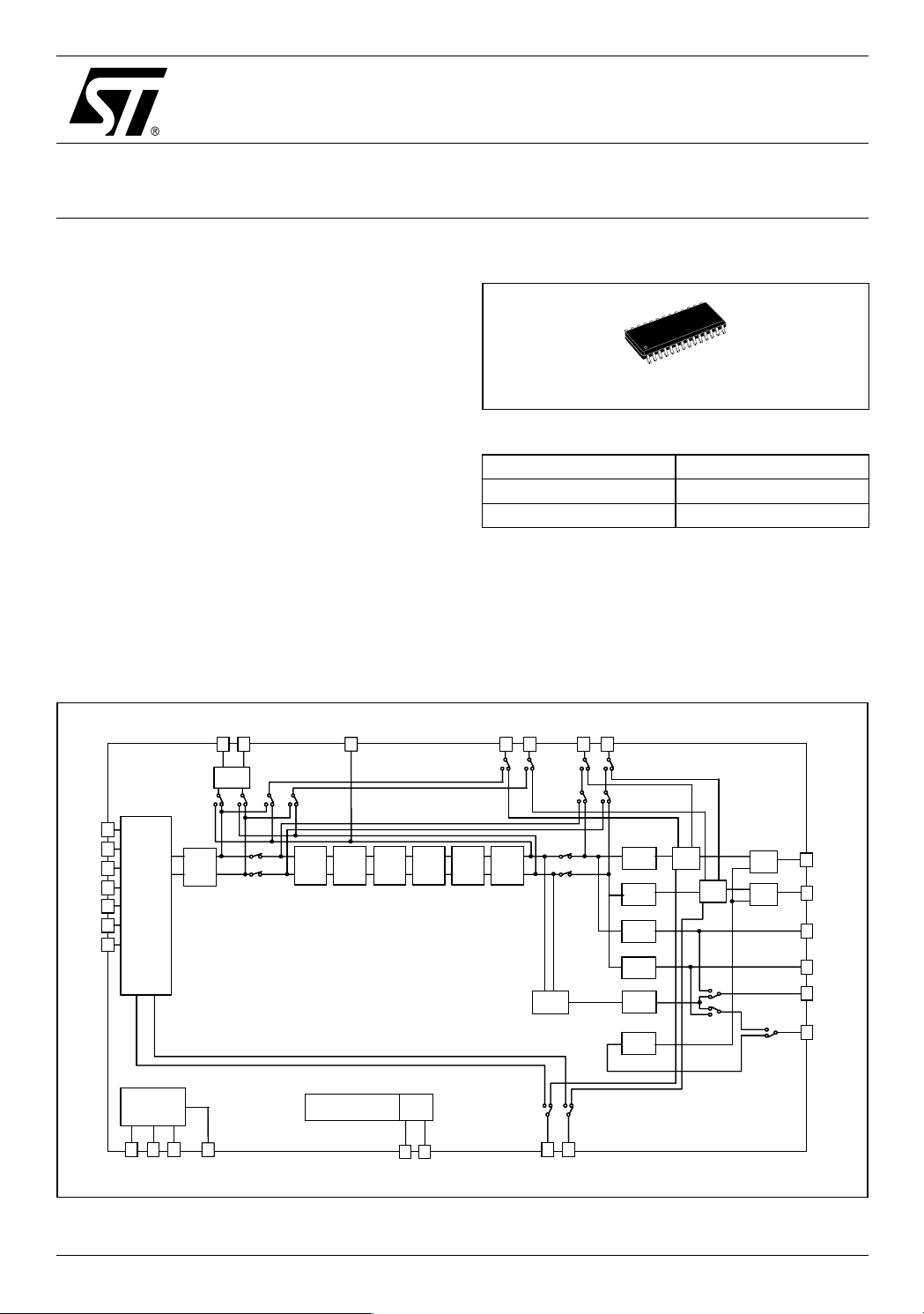
gure 1. Package
SO-28
Table 1. Order Codes
Part Number Package
TDA7419 SO-28
TDA7419TR SO-28 in Tape & Reel
cessor with fully integrated audio filters. The digital
control allows programming in a wide range of filter
characteristics. By the use of BICMOS-process and
linear signal processing low distortion and low noise
are obtained.
ACOUTL/
ACOUTR/
ACINL/
ACOUTL/
AC2OUTL
AC2OUTL
ACOUTR/
AC2OUTR
AC2OUTR
ACINL/
FILOL
FILOL
ACINR/
ACINR/
FILOR
FILOR
DIFFL
DIFFL
DIFFG
DIFFG
DIFFR
DIFFR
SE1L
SE1L
SE1R
SE1R
MULTIPLEXER
MULTIPLEXER
SE2L
SE2L
SE2R
SE2R
VDD CREFGND
VDD CREFGND
March 2005
INPUT
INPUT
SUPPLY
SUPPLY
InGain
InGain
AutoZero
AutoZero
VREFOUTF
VREFOUTF
Loudness MiddleTreble BassSoftMute
Loudness MiddleTreble BassSoftMute
DIGITAL CONTROL
DIGITAL CONTROL
DIGITAL CONTROL
Softstep
Softstep
Volume
Volume
I2C BUS
I2C BUS
I2C BUS
Softstep
Softstep
HPF
Softstep
Softstep
Softstep
Softstep
Softstep
Softstep
Softstep
Softstep
Softstep
Softstep
HPF
MonoFader
MonoFader
MonoFader
MonoFader
MonoFader
MonoFader
MonoFader
MonoFader
Subwoofer
Subwoofer
LPF
LPF
AC2INL/
SDASCL
SDASCL
AC2INL/
SE3L
SE3L
AC2INR/
AC2INR/
SE3R
SE3R
MonoFader
MonoFader
MonoFader
MonoFader
HPF
HPF
Mix
Mix
Mix
Mix
OUTLF
OUTLF
OUTRF
OUTRF
OUTLR
OUTLR
OUTRR
OUTRR
OUTSW/
OUTSW/
OUTLR2
OUTLR2
MIX/
MIX/
OUTSW/
OUTSW/
OUTRR2
OUTRR2
Rev. 2
1/30
Page 2
TDA7419
Table 2. Supply
Symbol Parameter Test Condition Min. Typ. Max. Unit
V
Supply Voltage 7.5 8.5 10.5 V
s
Supply Current Vs = 8.5V 30 35 40 mA
I
s
SVRR Ripple Rejection @ 1KHz Audioprocessor(all Filters flat) 60 dB
Table 3. Thermal Data
Symbol Parameter Value Unit
R
Th j-pins
Thermal Resistance Junction-pins max 85 °C/W
Table 4. Absolute Maximum Ratings
Symbol Parameter Value Unit
V
Operating Supply Voltage 10.5 V
s
T
T
Operating Temperature Range -40 to 85 °C
amb
Storage Temperature Range -55 to +150 °C
stg
ESD
All pins are protected against ESD according to the MIL883 standard.
Figure 3. Pin connection (Top view)
ACOUTR/AC2OUTR
ACINR/FILOR
ACINL/FILOL
ACOUTL/AC2OUTL
SE3L/ACINL
SE3R/ACINR
SE2L
SE2R
SE1L OUTLF
SE1R OUTLR
DIFFL
DIFFG
DIFFR OUTSW/OUTLR2
2
3
4
5
6
7
8
9
10
12
13
28
27
26
25
24
23
22
21
20
19
18
17
16
1514CREF GND
D04AU1569
MIX/OUTSW/OUTRR21
VREF
SAOUT
SAIN
VDD
SDA
SCL
MUTE
OUTRR11
OUTRF
2/30
Page 3
Table 5. Pin Description
TDA7419
Pin
N#
1 ACOUTR / AC2OUTR AC coupling right output / DSO filter AC2OUT right channel O
2 ACINR / FILOR AC coupling right input / DSO filter FILO right channel I/O
3 ACINL / FILOL AC coupling left input / DSO filter FILO left channel I/O
4 ACOUTL / AC2OUTL AC coupling left output / DSO filter AC2OUT left channel O
5 SE3L / ACINL Single-ended input 3 left channel / AC coupling left input I
6 SE3R / ACINR Single-ended input 3 right channel / AC coupling right input I
7 SE2L Single-ended input 2 left channel I
8 SE2R Single-ended input 2 right channel I
9 SE1L Single-ended input 1 left channel I
10 SE1R Single-ended input 1 Right channel I
11 DIFFL Pseudo differential stereo input left I
12 DIFFG Pseudo differential stereo input common I
13 DIFFR Pseudo differential stereo input right I
14 CREF Reference capacitor O
15 GND Ground S
16 OUTSW / OUTLR2
17 OUTRF Front right output O
18 OUTRR Rear right output O
19 OUTLR Rear left output O
20 OUTLF Front left output O
21 MUTE External mute pin I
22 SCL I2C bus clock I
23 SDA I2C bus data I/O
24 VDD Supply S
25 SAIN Spectrum analyzer clock input I
26 SAOUT Spectrum analyzer output O
27 VREF Vref output O
28 MIX / OUTSW / OUTRR2
Pin Name Function I/O
Subwoofer output / 2
Mix input / Additional subwoofer output / 2
nd
rear left output
nd
rear right output
O
I/O
3/30
Page 4

TDA7419
3 Audio Processor Features:
Input Multiplexer QD / SE: quasi-differential stereo inputs, with selectable single-ended mode
SE1: stereo single-ended input
SE2: stereo single-ended input
SE3 / AC2IN: stereo single-ended input / DSO filter input
In-Gain 0 to 15dB, 1dB steps
internal offset-cancellation (AutoZero)
separate second source-selector
Mixing stage mixable to front speaker-outputs
Loudness 2nd order frequency response
programmable center frequency (400Hz/800Hz/2400Hz)
15dB with 1dB steps
selectable low & high frequency boost
selectable flat-mode (constant attenuation)
Volume +15dB to -79dB with 1dB step resolution
soft-step control with programmable blend times
Bass 2nd order frequency response
center frequency programmable in 4 steps (60Hz/80Hz/100Hz/200Hz)
Q programmable 1.0/1.25/1.5/2.0
DC gain programmable
-15 to 15dB range with 1dB resolution
Middle 2nd order frequency response
center frequency programmable in 4 steps (500Hz/1KHz/1.5KHz/2.5KHz)
Q programmable 0.5/0.75/1.0/1.25
DC gain programmable
-15 to 15dB range with 1dB resolution
Treble 2nd order frequency response
center frequency programmable in 4 steps (10KHz/12.5KHz/15KHz/17.5KHz)
-15 to 15dB range with 1dB resolution
Spectrum analyzer seven bandpass filters
2nd order frequency response
programmable Q factor for different visual appearance
analog output
controlled by external serial clock
Speaker 4 independent soft step speaker controls, +15dB to -79dB with 1dB steps
Independent programmable mix input with 50% mixing ratio for front speakers
direct mute
Subwoofer 2nd order low pass filter with programmable cut off frequency
single-ended mono output
independent soft step level control, +15dB to -79dB with 1dB steps
Mute Functions direct mute
digitally controlled SoftMute with 3 programmable mute-times(0.48ms/0.96ms/
123ms)
Effect gain effect, or high pass effect with fixed external components
4/30
Page 5
TDA7419
4 ELECTRICAL CHARACTERISTICS
Table 6. Electrical Characteristcs
V
= 8.5V; T
S
Symbol Parameter Test Condition Min. Typ. Max. Unit
SUPPLY
Vs Supply Voltage 8 8.5 10 V
I
S
INPUT SELECTOR
R
in
V
CL
S
IN
G
IN MIN
G
IN MAX
G
STEP
V
DC
V
offset
DIFFERENTIAL STEREO INPUTS
R
in
CMRR Common Mode Rejection Ratio V
e
No
MIXING CONTROL
M
LEVEL
G
MAX
A
MAX
A
STEP
LOUDNESS CONTROL
A
MAX
A
STEP
f
Peak
VOLUME CONTROL
G
MAX
A
MAX
A
STEP
E
A
E
T
V
DC
= 25°C; RL= 10kΩ ; all gains = 0dB; f = 1kHz; unless otherwise specified
amb
Supply Current 27 37 47 mA
Input Resistance All single ended inputs 70 100 130 kΩ
Clipping level All Input 1.8 2 V
QD input 1.7 2 V
Input Separation 80 100 dB
Min. Input Gain -1 0 1 dB
Max. Input Gain 13 15 17 dB
Step Resolution 0.5 1 1.5 dB
DC Steps Adjacent Gain Steps -5 1 5 mV
G
MIN
to G
MAX
-20 4 20 mV
Remaining offset with AutoZero 0.5 mV
Input Resistance Differential 70 100 130 KΩ
=1 VRMS@ 1kHz 46 70 dB
CM
=1 VRMS@ 10kHz 46 60 dB
V
CM
Output Noise @ Speaker Outputs 20Hz-20kHz,flat;all stages 0dB 12 µV
Mixing Ratio Main / Mix Source -6/-6 dB
Max Gain 13 15 17 dB
Max Attenuation -83 -79 -75 dB
Step Resolution 0.5 1 1.5 dB
Max Attenuation -17 -15 -13 dB
Step Resolution 0.5 1 1.5 dB
Peak Frequency
f
P1
f
P2
f
P3
360 400 440 Hz
720 800 880 Hz
2200 2400 2600 Hz
Max Gain 13 15 17 dB
Max Attenuation -83 -79 -75 dB
Step Resolution 0.5 1 1.5 dB
Attenuation Set Error G = -20 to +20dB -0.75 0 +0.75 dB
G = -79 to -20dB -4 0 3 dB
Tracking Error 2dB
DC Steps Adjacent Attenuation Steps -3 0.1 3 mV
From 0dB to G
MIN
-5 0.5 5 mV
RMS
RMS
5/30
Page 6
TDA7419
Table 6. Electrical Characteristcs (continued)
V
= 8.5V; T
S
Symbol Parameter Test Condition Min. Typ. Max. Unit
SOFT MUTE
A
MUTE
T
D
V
TH Low
V
TH High
R
PU
V
PU
BASS CONTROL
Fc Center Frequency f
Q
BASS
C
RANGE
A
STEP
DC
GAIN
MIDDLE CONTROL
C
RANGE
A
STEP
f
c
Q
BASS
TREBLE CONTROL
C
RANGE
A
STEP
fc Center Frequency f
= 25°C; RL= 10kΩ ; all gains = 0dB; f = 1kHz; unless otherwise specified
amb
Mute Attenuation 80 100 dB
Delay Time T1 0.48 1 ms
T2 0.96 2 ms
T3 70 123 170 ms
Low Threshold for SM Pin 1 V
High Threshold for SM Pin 2.5 V
Internal pull-up resistor 32 45 58
Internal pull-up Voltage 3.3 V
54 60 66 Hz
72 80 88 Hz
90 100 110 Hz
180 200 220 Hz
0.911.1
1.11.251.4
1.3 1.5 1.7
1.822.2
Quality Factor Q
C1
f
C2
f
C3
f
C4
1
Q
2
Q
3
Q
4
Control Range ±14 ±15 ±16 dB
Step Resolution 0.5 1 1.5 dB
Bass-DC-Gain DC = off -1 0 +1 dB
DC = on (shelving filter, use for
-4.4 dB
cut only)
Control Range ±14 ±15 ±16 dB
Step Resolution 0.5 1 1.5 dB
Center Frequency f
Quality Factor Q
C1
f
C2
f
C3
f
C4
1
Q
2
Q
3
Q
4
400 500 600 Hz
0.811.2kHz
1.2 1.5 1.8 kHz
22.53kHz
0.45 0.5 0.55
0.65 0.75 0.85
0.911.1
1.11.251.4
Clipping Level ±14 ±15 ±16 dB
Step Resolution 0.5 1 1.5 dB
C1
f
C2
f
C3
f
C4
81012kHz
10 12.5 15 kHz
12 15 18 kHz
14 17.5 21 kHz
kΩ
6/30
Page 7
TDA7419
Table 6. Electrical Characteristcs (continued)
V
= 8.5V; T
S
Symbol Parameter Test Condition Min. Typ. Max. Unit
SPEAKER ATTENUATORS
G
MAX
A
MAX
A
STEP
A
MUTE
E
E
V
DC
AUDIO OUTPUTS
V
CL
R
OUT
R
L
C
L
V
DC
SUBWOOFER ATTENUATOR
G
MAX
A
MAX
A
STEP
A
MUTE
E
E
V
DC
SUBWOOFER LOWPASS
f
LP
HPF EFFECT
G
MAX
G
MIN
A
STEP
SPECTRUM ANALYZER CONTROL
V
SAOut
f
C1
f
C2
f
C3
f
C4
f
C5
f
C6
f
C7
Q Quality Factor Q1 1.62 1.8 1.98
f
SAClk
t
Sadel
= 25°C; RL= 10kΩ ; all gains = 0dB; f = 1kHz; unless otherwise specified
amb
Max Gain 14 15 16 dB
Max Attenuation -83 -79 -75 dB
Step Resolution 0.5 1 1.5 dB
Mute Attenuation 80 90 dB
Attenuation Set Error 2 dB
DC Steps Adjacent Attenuation Steps -5 0.1 5 mV
Clipping level d = 0.3% 1.8 2 V
Output impedance 30 100 Ω
Output Load Resistance 2 kΩ
Output Load Capacitor 10 nF
DC Voltage Level 3.8 4.0 4.2 V
Max Gain 14 15 16 dB
Max Attenuation -83 -79 -75 dB
Step Resolution 0.5 1 1.5 dB
Mute Attenuation 80 90 dB
Attenuation Set Error 2 dB
DC Steps Adjacent Attenuation Steps -5 1 5 mV
Lowpass Corner Frequency f
f
f
LP1
LP2
LP3
72 80 88 Hz
108 120 132 Hz
144 160 176 Hz
Max Gain 21 22 23 dB
Min Gain 3 4 5 dB
Step Resolution 1.5 2 2.5 dB
Output Voltage Range 0 3.3 V
Center Frequency Band 1 5.5 62 69 Hz
Center Frequency Band 2 141 157 173 Hz
Center Frequency Band 3 356 392 436 Hz
Center Frequency Band 4 0.9 1 1.1 kHz
Center Frequency Band 5 2.26 2.51 2.76 kHz
Center Frequency Band 6 5.70 6.34 6.98 kHz
Center Frequency Band 7 14.4 16 17.6 kHz
Q2 3.15 3.5 3.85
Clock Frequency 3 100 kHz
Analog Output Delay Time 2 µs
RMS
7/30
Page 8
TDA7419
Table 6. Electrical Characteristcs (continued)
V
= 8.5V; T
S
Symbol Parameter Test Condition Min. Typ. Max. Unit
t
repeat
t
intres
GENERAL
e
NO
S/N Signal to Noise Ratio all gain = 0dB flat; V
DDistortion V
S
C
= 25°C; RL= 10kΩ ; all gains = 0dB; f = 1kHz; unless otherwise specified
amb
Spectrum Analyzer Repeat Time 50 ms
Internal Reset Time 4.5 ms
Output Noise BW=20Hz to 20 kHz all gain =
12 20 µV
0dB
BW=20Hz to 20 kHz Output
615µV
muted
= 1V
IN
=2V
o
RMS
; all stages 0dB 0.01 0.1 %
RMS
100 dB
Channel Separation left/right 80 90 dB
5 DESCRIPTION OF THE AUDIOPROCESSOR
5.1 Input stages
In the basic configuration, one stereo quasi-differential and three (two in case of DSO applications) single
ended stereo inputs are available.
5.1.1 Quasi-differential stereo Input (QD)
The QD input is implemented as a buffered quasi-differential stereo stage with 100k input-impedance at
each input. The attenuation is fixed to -3dB in order to adapt the incoming signal level.
5.1.2 Single-ended stereo input (SE1, SE2, SE3/AC2IN)
The input-impedance at each input is 100k and the attenuation is fixed to -3dB for incoming signals. The
input for SE3 is also configurable as part of the interface for external filters in DSO applications (AC2IN)
Figure 4. Input Stage
QD_L
QD_G
QD_R
SE1_L
SE1_R
SE2_L
SE2_R
AC2IN_L/SE3L
AC2IN_R/SE3R
QD
SE1
SE2
SE3
QD
SE4
SE1
SE2
SE3
Main
Source
In Gain
8/30
Second
Source
Output Stage
Page 9
TDA7419
5.2 AutoZero
The AutoZero allows a reduction of the number of pins as well as external components by canceling any
offset generated by or before the In-Gain-stage (Please notice that externally generated offsets, e.g. generated through the leakage current of the coupling capacitors, are not canceled).
The auto-zeroing is started every time the input source is changed and needs max. 0.3ms for the alignment. To avoid audible clicks the Audio processor is muted before the loudness stage during this time.
The AutoZero feature is only present in the main signal-path.
5.2.1 AutoZero-Remain
In some cases, for example if the P is executing a refresh cycle of the IIC-Bus-programming, it is not useful to start a new AutoZero-action because no new source is selected and an undesired mute would appear at the outputs. For such applications, it can be switched in the AutoZero-Remain-Mode (Bit 6 of the
subaddress-byte). If this bit is set to high, the AutoZero will not be invoked and the old adjustment-value
remains.
5.3 Loudness
There are four parameters programmable in the loudness stage:
5.3.1 Attenuation
Figure 5 shows the attenuation as a function of frequency at f
= 400Hz
P
Figure 5. Loudness Attenuation @ f
5
0
-5
-10
-15
-20
10
= 400Hz.
P
100
1K
10K
9/30
Page 10
TDA7419
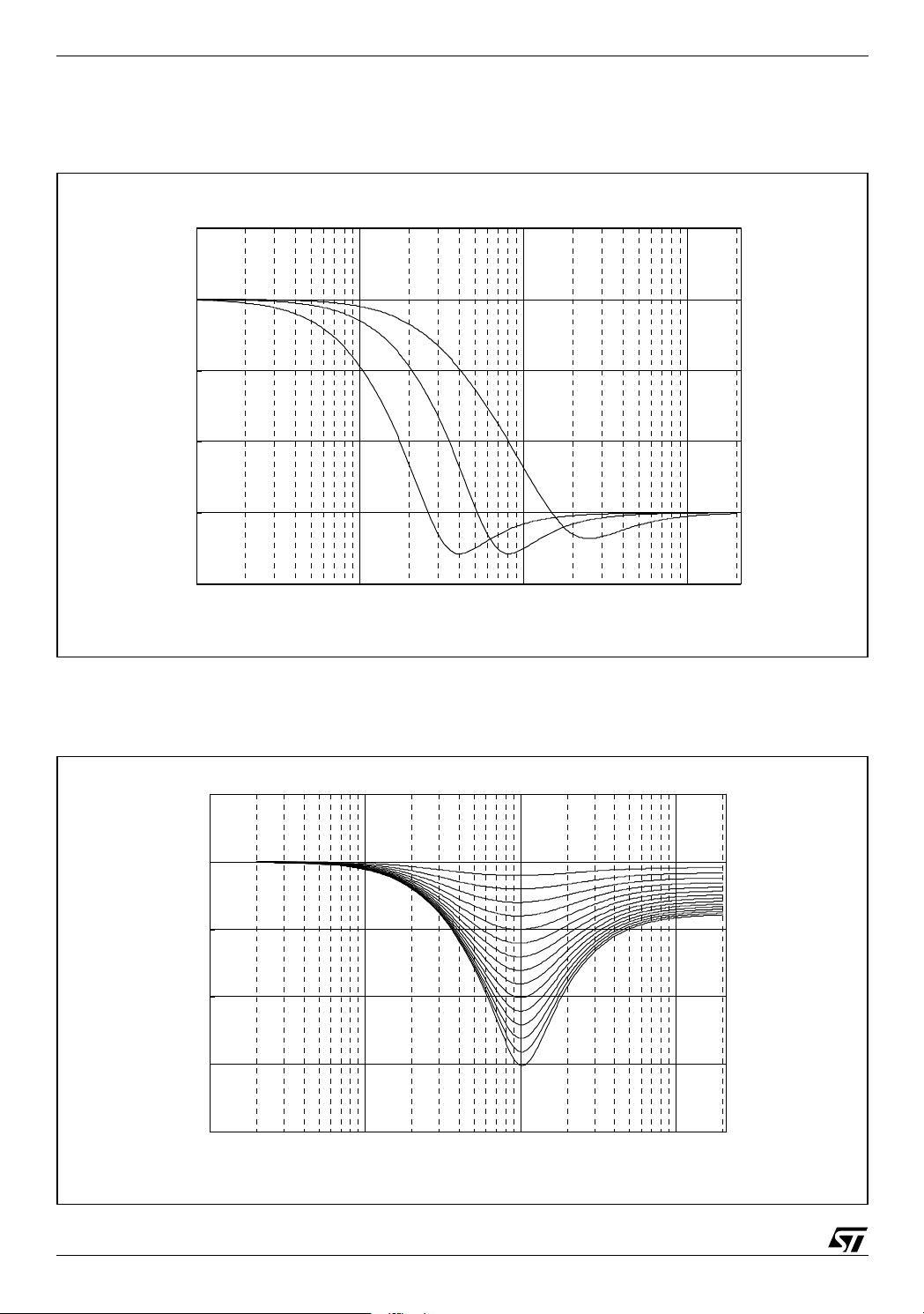
5.3.2 Peakr Frequency
Figure 6 shows the three possible peak-frequencies 400Hz , 800Hz and 2.4kHz.
Figure 6. Loudness Center frequencies @ Attn. = 15dB
5
0
-5
-10
-15
-20
10
100
1K
5.3.3 Low & High Frequency Boost
Figure 7 shows the different Loudness-shapes in low & high frequency boost.
Figure 7. Loudness Attenuation , fC = 2.4KHz
5
0
-5
-10
-15
10K
10/30
-20
10
100
1K
10K
Page 11

5.3.4 Flat Mode
In flat mode the loudness stage works as a 0dB to -15dB attenuator.
TDA7419
5.4 SoftMute
2
The digitally controlled SoftMute stage allows muting/demuting the signal with a I
slope. The mute process can either be activated by the SoftMute pin or by the I
C-bus programmable
2
C-bus. This slope is real-
ized in a special S-shaped curve to mute slow in the critical regions (see Figure 8).
For timing purposes the Bit0 of the I2C-bus output register is set to 1 from the start of muting until the end
of demuting.
Figure 8. Sofmute Timing
1
EXT.
MUTE
+SIGNAL
REF
-SIGNAL
1
2
I
C BUS
OUT
D97AU634
Time
Note: Please notice that a started Mute-action is always terminated and could not be interrupted by a change of the mute -signal
5.5 SoftStep-Volume
When the volume-level is changed audible clicks could appear at the output. The root cause of those clicks
could either be a DC-Offset before the volume-stage or the sudden change of the envelope of the audiosignal. With the SoftStep feature both kinds of clicks could be reduced to a minimum and are no more
audible. The blend-time from one step to the next is programmable in four steps.
Figure 9. SoftStep Timing
V
OUT
1dB
0.5dB
SS Time
-0.5dB
-1dB
Note: For steps more than 0.5dB the SoftStep mode should be deactivated because it could generate a hard 1dB step during the blend-time.
D00AU1170
Time
11/30
Page 12

TDA7419
5.6 Bass
There are four parameters programmable in the bass stage:
5.6.1 Attenuation
Figure 9 shows the attenuation as a function of frequency at a center frequency of 80Hz.
Figure 10. Bass Control @ f
15.0
10.0
5.0
= 80Hz, Q = 1
C
dB
0.0
-5.0
-10.0
-15.0
10.0 100.0 1.0K 10.0K
Hz
5.6.2 Center Frequency
Figure 11 shows the four possible center frequencies 60, 80, 100 and 200Hz.
Figure 11. Bass center Frequencies @ Gain = 15dB, Q = 1
16
12
8
4
0
-4
10
12/30
100
1K
10K
Page 13

5.6.3 Quality Factors
Figure 12 shows the four possible quality factors 1, 1.25, 1.5 and 2.
Figure 12. Bass Quality factors @ Gain = 14dB, fC = 80Hz
15.0
12.5
10.0
7.5
5.0
2.5
TDA7419
0.0
10.0 100.0 1.0K 10.0K
5.6.4 DC Mode
It is used for cut only for shelving filter. In this mode the DC-gain is increased by 4.4dB. Inaddition the programmed center frequency and quality factor is decreased by 25% which can be used to reach alternative center frequencies or quality factors.
Figure 13. Bass normal and DC Mode @ Gain = 14dB, fC = 80Hz
15.0
12.5
10.0
7.5
5.0
2.5
0.0
10.0 100.0 1.0K 10.0K
Note: The center frequency, Q and DC-mode can be set fully independently.
13/30
Page 14

TDA7419
5.7 Middle
There are three parameters programmable in the middle stage:
5.7.1 Attenuation
Figure 14 shows the attenuation as a function of frequency at a center frequency of 1kHz.
Figure 14. Middle Control @ f
= 1 kHz, Q = 1
C
5.7.2 Center Frequency
Figure 14 shows the four possible center frequencies 500Hz, 1kHz, 1.5kHz and 2.5kHz.
Figure 15. Middle center Frequencies @ Gain = 14dB, Q = 1
14/30
Page 15

5.7.3 Quality Factors
Figure 16 shows the four possible quality factors 0.5, 0.75, 1 and 1.25.
Figure 16. Middle Quality factors @ Gain = 14dB, fc = 1kHz
TDA7419
5.8 Treble
There are two parameters programmable in the treble stage:
5.8.1 Attenuation
Figure 16 shows the attenuation as a function of frequency at a center frequency of 17.5kHz.
Figure 17. Treble Control @ f
20
15
10
5
0
-5
-10
-15
= 17.5kHz
C
-20
10
100
1K
10K
15/30
Page 16

TDA7419
5.8.2 Center Frequency
Figure 18 shows the four possible center frequencies 10k, 12.5k, 15k and 17.5kHz.
Figure 18. Treble Center Frequencies @ Gain = 15dB
20
15
10
5
0
-5
10
100
1K
10K
5.9 Subwoofer Filter
The subwoofer lowpass filter has butterworth characteristics with programmable cut-off frequency (80/
120/160Hz)
Figure 19. Subwoofer Control
16/30
Page 17

TDA7419
5.10 Spectrum Analyzer
A fully integrated seven-band spectrum analyzer with programmable quality factor is present. The spectrum analyzer consists of seven band pass filters with rectifier and sample capacitor that stores the maximum peak signal level since the last read cycle. This peak signal level can be read by a microprocessor
at the SAout-pin. To allow easy interfacing to an analog port of the microprocessor, the output voltage at
this pin is referred to device ground.
The microprocessor starts a read cycle with the negative going clock edge at the SAclk input. On the following positive clock edges, the peak signal level for the band pass filters is subsequently switched to
SAout. Each analog output data is valid after the time t
whenever SAclk remains high for the time t
. Note that a proper reset requires the clock signal SAclk
intres
to be held at high potential. Figure 20 shows the block diagram and figure 21 illustrates the read cycle
timing of the spectrum analyzer.
Figure 20. Spectrum analyzer block diagram
. A reset of the sample capacitors is induced
Sadel
Figure 21. Timing of the spectrum analyzer
17/30
Page 18

TDA7419
5.11 AC-Coupling
In some applications additional signal manipulations are desired, such as additional band equalizations.
For this purpose, an AC-Coupling can be placed before the loudness attenuator or speaker-attenuators,
which can be activated or internally shorted by I
attenuator is available at the AC-Outputs. The input-impedance of this AC-Inputs is 50kΩ.
Figure 22. Diagram of AC coupling
2
C-Bus. In short condition, the input-signal of the speaker-
ACINR
Speakers
To Output
From Input MUX
InGain
ACOUTR ACOUTL
Filters
ACINL
5.12 DSO Applications
For DSO applications, DSO filter is available for additional processing after the speaker control. It is a 2nd
order Butterworth highpass filter with selectable flat mode. Figure 23 shows the diagram of the DSO that
includes an external RC network.
Figure 23. DSO diagram
External RC network
From speaker
18/30
ACOUT
/AC2OUT
SE3IN
/AC2IN
ACIN
/FILO
Gain Control
To
output
Page 19

TDA7419
5.13 Output Selector and Mixing
The output-selector allows the front and rear speakers to connect to different sources. The setup of the
output selector is shown in Figure 24. A Mixing-stage is placed after the front speaker-attenuator and can
be set to mixing-mode. Having a full volume-attenuator for the mix-signal, the stage offers a wide flexibility
to adapt the mixing levels.
Figure 24. Output Selector
Mix_in
Attenuator
Main
Second
BassL+BassR
Attenuator
Attenuator
Subwoofer
filter
Attenuator
Front
Rear
Subwoofer
output
5.14 Audioprocessor Testing
In the test mode, which can be activated by setting bit D7 of the IIC subaddress byte and bit D0 of the
testing audioprocessor byte, several internal signals are available at the SE1R pin. In this mode, the input
resistance of 100kOhm is disconnected from the pin. Internal signals available for testing are listed in the
data-byte specification.
5.15 Test Circuit
Figure 25. Test Circuit
19/30
Page 20

TDA7419
6I2C BUS SPECIFICATION
6.1 Interface Protocol
The interface protocol comprises:
– a start condition (S)
– a chip address byte (the LSB determines read/write transmission)
– a subaddress byte
– a sequence of data (N-bytes + acknowledge)
– a stop condition (P)
– the max. clock speed is 500kbits/s
– 3.3V logic compatible
6.1.1 Receive Mode
S 1 0 0 0 1 0 0 R/W ACK TS AZ AI A4 A3 A2 A1 A0 ACK DATA ACK P
S = Start
R/W = "0" -> Receive Mode (Chip can be programmed by µP)
"1" -> Transmission Mode (Data could be received by µP)
ACK = Acknowledge
P = Stop
TS = Testing mode
AZ = Auto zero remain
AI = Auto increment
6.1.2 Transmission Mode
1 0 0 0 1 0 0 R/W ACK X X X X X X X SM ACK P
S
SM = Soft mute activated for main channel
X = Not Used
The transmitted data is automatic updated after each ACK. Transmission can be repeated without new
chip address.
6.1.3 Reset Condition
A Power-On-Reset is invoked if the Supply-Voltage is below than 3.5V. After that the following data is written automatically into the registers of all subaddresses:
MSB LSB
11111110
20/30
Page 21

6.2 Subaddress (receive mode)
Table 7. Subaddress (receive mode)
MSB LSB FUNCTION
I2 I1 I0 A4 A3 A2 A1 A0
Testing Mode
0
1
0
1
0
1
0 0 0 0 0 Main Source Selector
0 0 0 0 1 Main Loudness
0 0 0 1 0 Soft Mute / Clock Generator
0 0 0 1 1 Volume
001 0 0Treble
0 0 1 0 1 Middle
001 1 0Bass
0 0 1 1 1 Second Source Selector
0 1 0 0 0 Subwoofer / Middle / Bass
0 1 0 0 1 Mixing / Gain Effect
0 1 0 1 0 Speaker Attenuator Left Front
0 1 0 1 1 Speaker Attenuator Right Front
0 1 1 0 0 Speaker Attenuator Left Rear
0 1 1 0 1 Speaker Attenuator Right Rear
0 1 1 1 0 Mixing Level Control
0 1 1 1 1 Subwoofer Attenuator
1 0 0 0 0 Spectrum Analyzer / Clock Source / AC Mode
1 0 0 0 1 Testing Audio Processor
Off
On
Auto Zero Remain
Off
On
Auto Increment Mode
Off
On
TDA7419
21/30
Page 22

TDA7419
6.3 Data Byte Specification
Table 8. Main Selector (0)
MSB LSB FUNCTION
D7 D6 D5 D4 D3 D2 D1 D0
Source Selector
QD/SE: QD
0
0
0
0
1
1
1
0
0
:
1
1
0
1
0
0
:
1
1
0
0
:
1
1
0
1
:
0
1
0
0
1
1
0
0
1
0
1
0
1
0
1
x
SE1
SE2
SE3
QD/SE: SE
mute
mute
Input Gain
0dB
1dB
:
14dB
15dB
Auto Zero
on
off
Table 9. Main Loudness (1)
MSB LSB FUNCTION
D7 D6 D5 D4 D3 D2 D1 D0
Attenuation
0dB
0
0
:
1
1
0
0
1
1
0
1
0
1
0
1
0
1
0
0
:
1
1
0
0
:
1
1
0
-1dB
1
:
:
-14dB
0
-15dB
1
Center Frequency
Flat
400Hz
800Hz
2400Hz
High Boost
on
off
Loudness Soft Step
on
off
22/30
Page 23

Table 10. Soft Mute / Clock Generator (2)
MSB LSB FUNCTION
D7 D6 D5 D4 D3 D2 D1 D0
Soft Mute
0
on
1
off
Pin Influence for Mute
0
1
0
0
1
0
0
0
0
1
1
1
1
0
1
0
0
1
1
0
0
1
1
0
1
0
1
0
1
0
1
0
1
x
Pin and IIC
IIC
Soft Mute Time
0.48ms
0.96ms
123ms
Soft Step Time
0.160ms
0.321ms
0. 642ms
1.28ms
2.56ms
5.12ms
10.24ms
20.48ms
Clock Fast Mode
on
off
TDA7419
Table 11. Volume / Speaker / Mixing / Subwoofer Attenuation (3, 10-15)
MSB LSB FUNCTION
D7 D6 D5 D4 D3 D2 D1 D0
Gain/Attenuation
+0dB
0
0
:
0
0
0
:
1
1
1
0
1
0
0
:
0
0
0
:
0
0
1
0
0
:
0
1
1
:
1
1
x
0
0
:
1
0
0
:
1
1
x
0
0
:
1
0
0
:
1
1
x
0
0
:
1
0
0
:
1
1
x
0
1
:
1
0
1
:
0
1
x
+1dB
:
+15dB
-0dB
-1dB
:
-78dB
-79dB
mute
Soft Step
on
off
23/30
Page 24

TDA7419
Table 12. Treble Filter (4)
MSB LSB FUNCTION
D7 D6 D5 D4 D3 D2 D1 D0
Gain/Attenuation
-15dB
0
0
:
0
0
1
1
:
1
1
0
0
1
1
0
1
0
1
0
1
1
1
:
0
0
0
0
:
1
1
1
1
:
0
0
0
0
:
1
1
1
1
:
0
0
0
0
:
1
1
1
-14dB
0
:
:
-1dB
1
0dB
0
0dB
0
+1dB
1
:
:
+14dB
0
+15dB
1
Treble Center Frequency
10.0kHz
12.5kHz
15.0kHz
17.5kHz
Reference Output Select
External Vref (4V)
Internal Vref (3.3V)
Table 13. Middle Filter (5)
MSB LSB FUNCTION
D7 D6 D5 D4 D3 D2 D1 D0
Gain/Attenuation
-15dB
0
0
:
0
0
1
1
:
1
1
0
0
1
1
0
1
0
1
0
1
1
1
:
0
0
0
0
:
1
1
1
1
:
0
0
0
0
:
1
1
1
1
:
0
0
0
0
:
1
1
1
-14dB
0
:
:
-1dB
1
0dB
0
0dB
0
+1dB
1
:
:
+14dB
0
+15dB
1
Middle Q Factor
0.5
0.75
1
1.25
Middle Soft Step
on
off
24/30
Page 25

Table 14. Bass Filter (6)
MSB LSB FUNCTION
D7 D6 D5 D4 D3 D2 D1 D0
Gain/Attenuation
-15dB
0
0
:
0
0
1
1
:
1
1
0
0
1
1
0
1
0
1
0
1
1
1
:
0
0
0
0
:
1
1
1
1
:
0
0
0
0
:
1
1
1
1
:
0
0
0
0
:
1
1
1
-14dB
0
:
:
-1dB
1
0dB
0
0dB
0
+1dB
1
:
:
+14dB
0
+15dB
1
Bass Q Factor
1.0
1.25
1.5
2.0
Bass Soft Step
on
off
TDA7419
Table 15. Second Source Selector (7)
MSB LSB FUNCTION
D7 D6 D5 D4 D3 D2 D1 D0
Source Selector
QD/SE: QD
0
0
0
0
1
1
1
0
0
:
1
1
0
1
0
0
:
1
1
0
0
:
1
1
0
1
:
0
1
0
0
1
1
0
0
1
0
SE1
1
SE2
0
SE3
1
QD/SE: SE
0
mute
1
mute
x
Input Gain
0dB
1dB
:
14dB
15dB
Rear Speaker Source
main source
second source
25/30
Page 26

TDA7419
Table 16. Subwoofer /Middle / Bass (8)
MSB LSB FUNCTION
D7 D6 D5 D4 D3 D2 D1 D0
Subwoofer Cut-off Frequency
flat
0
0
1
1
0
0
1
1
0
0
1
1
0
1
0
1
0
1
0
1
0
1
0
1
0
80Hz
1
120Hz
0
160Hz
1
Middle Center Frequency
500Hz
1000Hz
1500Hz
2500Hz
Bass Center Frequency
60Hz
80Hz
100Hz
200Hz
Bass DC Mode
on
off
Smoothing Filter
on
off (bypass)
Table 17. Mixing / Gain Effect (9)
MSB LSB FUNCTION
D7 D6 D5 D4 D3 D2 D1 D0
Mixing to Left Front Speaker
0
on
1
off
0
1
0
1
0
1
0
0
:
1
1
1
1
0
0
:
0
0
0
1
0
0
:
0
0
1
x
0
1
:
0
1
x
x
Mixing to Right Front Speaker
on
off
Mixing Enable
on
off
Subwoofer Enable (OUTLR2 & OUTRR2)
on
off
Gain Effect for DSO Filter
4dB
6dB
:
20dB
22dB
0dB
0dB
26/30
Page 27

Table 18. Spectrum Analyzer / Clock Source / AC Mode (16)
MSB LSB FUNCTION
D7 D6 D5 D4 D3 D2 D1 D0
Spectrum Analyzer Filter Q Factor
0
3.5
1
1.75
0
1
0
1
0
1
0
1
0
1
0
0
1
1
0
1
0
1
Reset Mode
IIC
Auto
Spectrum Analyzer Source
Bass
InGain
Spectrum Analyzer Run
on
off
Reset
on
off
Clock Source
internal
external
Coupling Mode
DC Coupling (without DSO)
AC coupling after InGain
DC Coupling (with DSO)
AC coupling after Bass
TDA7419
Table 19. Testing Audio Processor (17)
MSB LSB FUNCTION
D7 D6 D5 D4 D3 D2 D1 D0
Audio Processor Testing Mode
off
0
on
1
Test Multiplexer
0
0
0
0
0
0
0
0
0
0
0
0
0
0
0
0
1
1
1
1
1
1
1
1
xx Not used
0
0
0
0
0
0
0
0
1
1
1
1
1
1
1
1
0
0
0
0
1
1
1
1
0
0
0
0
1
1
1
1
0
0
0
0
1
1
1
1
0
0
1
1
0
0
1
1
0
0
1
1
0
0
1
1
0
0
1
1
0
0
1
1
0
1
0
1
0
1
0
1
0
1
0
1
0
1
0
1
0
1
0
1
0
1
0
1
x
x
x
x
x
x
x
x
Left InGain
Left InGain
Left Loudness
Left Loudness
Left Volume
Left Volume
Left Treble
Left Treble
Left Middle
SMCLK
Left Bass
VrefSCR
VGB1.26
SSCLK
Clock200
Mon
Ref5V5
BPout<1>
BPout<2>
BPout<3>
BPout<4>
BPout<5>
BPout<6>
BPout<7>
27/30
Page 28

TDA7419
Figure 26. SO-28 Mechanical Data & Package Dimensions
DIM.
A 2.65 0.104
a1 0.1 0.3 0.004 0.012
b 0.35 0.49 0.014 0.019
b1 0.23 0.32 0.009 0.013
C 0.5 0.020
c1 45° (typ.)
D 17.7 18.1 0.697 0.713
E 10 10.65 0.394 0.419
e 1.27 0.050
e3 16.51 0.65
F 7.4 7.6 0.291 0.299
L 0.4 1.27 0.016 0.050
S8
mm inch
MIN. TYP. MAX. MIN. TYP. MAX.
(max.)
°
OUTLINE AND
MECHANICAL DATA
SO-28
28/30
Page 29

Table 20. Revision History
Date Revision Description of Changes
November 2004 1 First Issue
March 2005 2 Inserted new values in Electrical Characteristics
TDA7419
29/30
Page 30

TDA7419
Information furnished is believed to be accurate and reliable. However, STMicroelectronics assumes no responsibility for the consequences
of use of such information nor for any infringement of patents or other rights of third parties which may result from its use. No license is granted
by implication or otherwise under any patent or patent rights of STMicroelectronics. Specifications mentioned in this publication are subject
to change without notice. This publication supersedes and replaces all information previously supplied. STMicroelectronics products are not
authorized for use as critical components in life support devices or systems without express written approval of STMicroelectronics.
The ST logo is a registered trademark of STMicroelectronics.
All other names are the property of their respective owners
© 2005 STMicroelectronics - All rights reserved
Australia - Belgium - Brazil - Canada - China - Czech Republic - Finland - France - Germany - Hong Kong - India - Israel - Italy - Japan -
Malaysia - Malta - Morocco - Singapore - Spain - Sweden - Switzerland - United Kingdom - United States of America
STMicroelectronics group of companies
www.st.com
30/30
Page 31

 Loading...