

Page 1
®
TDA7294
100V - 100W DMOS AUDIO AMPLIFIER WITH MUTE/ST-BY
VERY HIG H OPERATI NG VOLTAGE R ANGE
(±40V)
DMOS POWER STAGE
HIGH OUTPUT POWER (UP TO 100W MU-
SIC POWER)
MUTING/STAND- BY FUNC TION S
NO SWITCH ON/OFF NOISE
NO BOUCHEROT CELLS
VERY LOW DISTORTION
VERY LOW NOISE
SHORT CIRCUIT PROTECTION
THERMAL SHUTDOWN
DESCRIPTION
The TDA7294 is a monolithic integrated circuit in
Multiwatt15 package, intended for use as audio
class AB amplifier in Hi-Fi field applications
(Home Stereo, self powered loudspeakers, Topclass TV). Thanks to the wide voltage range and
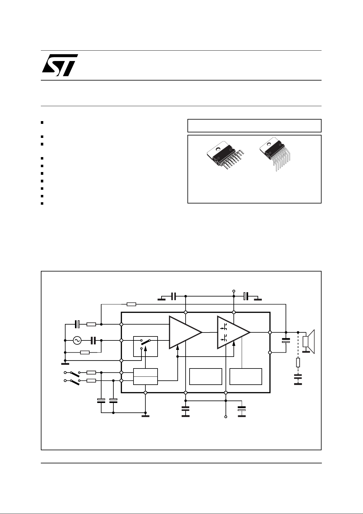
Figure 1: Typical Application and Test Circuit
MULTIPOWER BCD TECHNOLOGY
Multiwatt15V Multiwatt15H
ORDERING NUMBERS:
TDA7294V TDA7294HS
to the high out current c apability it is able to supply the highest power into both 4Ω and 8Ω loads
even in presence of poor supply regulation, with
high Supply Voltage Rejection.
The built in muting function with turn on delay
simplifies the remote operation avoiding switching
on-off noises.
+VsC7 100nF C6 1000µF
VM
VSTBY
April 2003
R3 22K
C2
R2
22µF
680Ω
C1 470nF
R1 22K
R5 10K
R4 22K
C3 10µF C4 10µF
Note: The Boucherot cell R6, C10, normally not necessary for a stable operation it could
be needed in presence of particular load impedances at V
IN- 2
IN+
IN+MUTE
MUTE
STBY
3
4
10
9
MUTE
STBY
1
STBY-GND
713
-
+
THERMAL
SHUTDOWN
-Vs -PWVs
C9 100nF C8 1000µF
<±25V.
S
+PWVs+Vs
PROTECTION
158
-Vs
S/C
14
OUT
C5
22µF
6
BOOTSTRAP
D93AU011
R6
2.7Ω
C10
100nF
1/17
Page 2
TDA7294
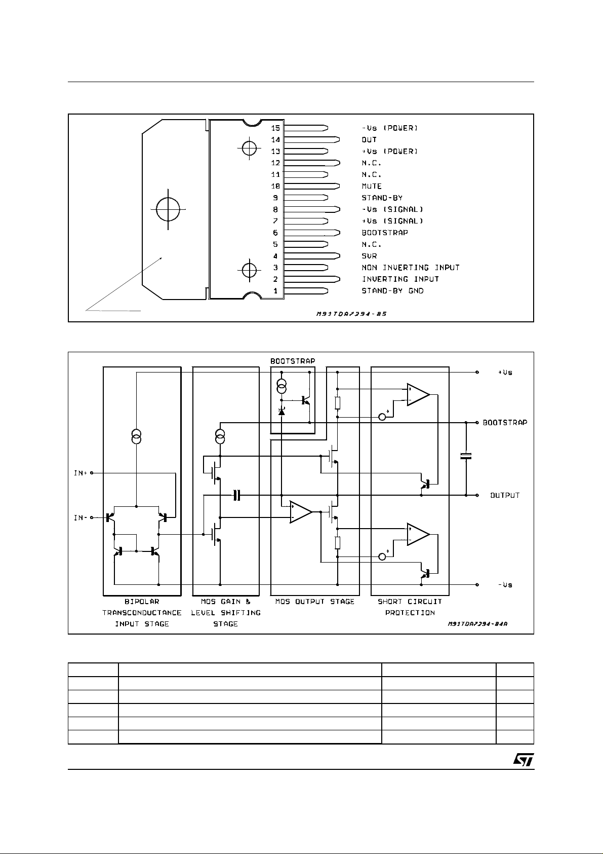
PIN CONNECTION (Top view)
TAB connected to -V
BLOCK DIAGRAM
S
ABSOLUTE MAXIMUM RATINGS
Symbol Parameter Value Unit
V
I
O
P
tot
T
op
T
stg
Supply Voltage (No Signal)
S
Output Peak Current 10 A
Power Dissipation T
= 70°C50W
case
Operating Ambient Temperature Range 0 to 70
, TjStorage and Junction Temperature 150
2/17
50 V
±
C
°
C
°
Page 3
TDA7294
THERMAL DATA
Symbol Description Value Unit
R
th j-case
Thermal Resistance Junction-case Max 1.5
C/W
°
ELECTRICAL CHARACTERISTICS (Refer to the Test Circuit V
= 50 Ω; T
R
g
= 25°C, f = 1 kHz; unless otherwise specified.
amb
= ±35V, RL = 8Ω, GV = 30dB;
S
Symbol Parameter Test Condition Min. Typ. Max. Unit
V
I
I
V
I
OS
P
Supply Range
S
Quiescent Current 20 30 65 mA
q
Input Bias Current 500 nA
b
Input Offset Voltage +10 mV
OS
Input Offset Current +100 nA
RMS Continuous Output Power d = 0.5%:
O
Music Power (RMS)
IEC268.3 RULES - ∆t = 1s (*)
d Total Harmonic Distortion (**) P
V
= ± 35V, RL = 8
S
V
= ± 31V, RL = 6
S
V
= ± 27V, RL = 4
S
Ω
Ω
Ω
d = 10%
R
= 8Ω ; VS = ±38V
L
R
= 6Ω ; VS = ±33V
L
R
= 4Ω ; VS = ±29V (***)
L
= 5W; f = 1kHz
O
P
= 0.1 to 50W; f = 20Hz to 20kHz
O
= ±27V, RL = 4
V
S
P
= 5W; f = 1kHz
O
P
= 0.1 to 50W; f = 20Hz to 20kHz
O
Ω:
10
±
60
60
60
70
70
70
100
100
100
0.005
0.01
40 V
±
0.1
0.1
W
W
W
W
W
W
%
%
%
%
SR Slew Rate 7 10 V/µs
G
G
e
, f
f
L
R
SVR Supply Voltage Rejection f = 100Hz; V
T
STAND-BY FUNCTION (Ref: -V
V
ST on
V
ST off
ATT
I
q st-by
MUTE FUNCTION (Ref: -V
V
Mon
V
Moff
ATT
Note (*):
MUSIC POWER CONCEPT
MUSIC POWER is the maximal power which the amplifier is capable of producing across the rated load resistance (regardless of non linearity)
1 sec after the application of a sinusoidal input signal of frequency 1KHz .
Note (**):
Note (***):
Open Loop Voltage Gain 80 dB
V
Closed Loop Voltage Gain 24 30 40 dB
V
Total Input Noise A = curve
N
f = 20Hz to 20kHz
Frequency Response (-3dB) PO = 1W 20Hz to 20kHz
H
Input Resistance 100 k
i
= 0.5Vrms 60 75 dB
ripple
Thermal Shutdown 145
S
or GND)
S
1
25
Stand-by on Threshold 1.5 V
Stand-by off Threshold 3.5 V
Stand-by Attenuation 70 90 dB
st-by
Quiescent Current @ Stand-by 1 3 mA
or GND)
S
Mute on Threshold 1.5 V
Mute off Threshold 3.5 V
Mute AttenuatIon 60 80 dB
mute
Tested with optimized Application Board (see fig. 2)
Limited by the max. allowable current.
V
µ
V
µ
Ω
C
°
3/17
Page 4
TDA7294
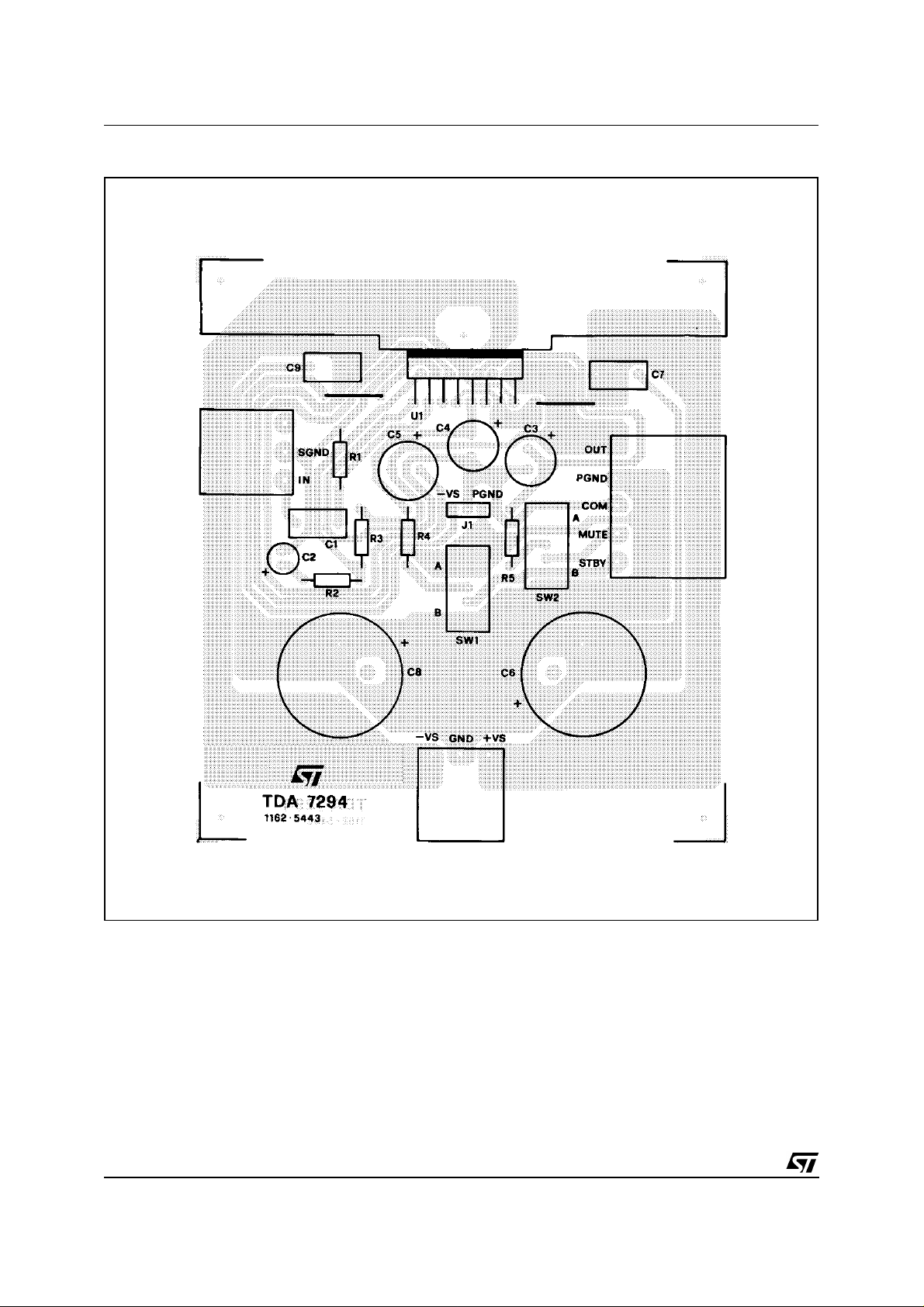
Figure 2: P.C.B. and components layout of the circuit of figure 1. (1:1 scale)
Note:
The Stand-by and Mute functions can be referred either to GND or -VS.
On the P.C.B. is possible to set both the configuration through the jumper J1.
4/17
Page 5

TDA7294
APPLICATION SUGGES TION S (see Test and Application Circuits of the Fig. 1)
The recommended values of t he external components are t hose shown on t he application circuit o f Figure 1. Different values can be used; the following table can help the designer.
COMPONENTS SUGGESTED VALUE PURPOSE
R1 (*) 22k INPUT RESISTANCE INCREASE INPUT
R2 680
R3 (*) 22k INCREASE OF GAIN DECREASE OF GAIN
R4 22k ST-BY TIME
R5 10k MUTE TIME
C1 0.47µF INPUT DC
C2 22µF FEEDBACK DC
C3 10µF MUTE TIME
C4 10µF ST-BY TIME
Ω
CLOSED LOOP GAIN
SET TO 30dB (**)
CONSTANT
CONSTANT
DECOUPLING
DECOUPLING
CONSTANT
CONSTANT
LARGER THAN
SUGGESTED
IMPRDANCE
DECREASE OF GAIN INCREASE OF GAIN
LARGER ST-BY
ON/OFF TIME
LARGER MUTE
ON/OFF TIME
LARGER MUTE
ON/OFF TIME
LARGER ST-BY
ON/OFF TIME
SMALLER THAN
SUGGESTED
DECREASE INPUT
IMPEDANCE
SMALLER ST-BY
ON/OFF TIME;
POP NOISE
SMALLER MUTE
ON/OFF TIME
HIGHER LOW
FREQUENCY
CUTOFF
HIGHER LOW
FREQUENCY
CUTOFF
SMALLER MUTE
ON/OFF TIME
SMALLER ST-BY
ON/OFF TIME;
POP NOISE
C5 22µF BOOTSTRAPPING SIGNAL
C6, C8 1000µF SUPPLY VOLTAGE
C7, C9 0.1µF SUPPLY VOLTAGE
(*) R1 = R3 FOR POP OPTIMIZATION
(**) CLOSED LOOP GAIN HAS TO BE ≥ 24dB
BYPASS
BYPASS
DEGRADATION AT
LOW FREQUENCY
DANGER OF
OSCILLATION
DANGER OF
OSCILLATION
5/17
Page 6
TDA7294
TYPICAL CHARACTERISTICS
(Application Circuit of fig 1 unless otherwise specified)
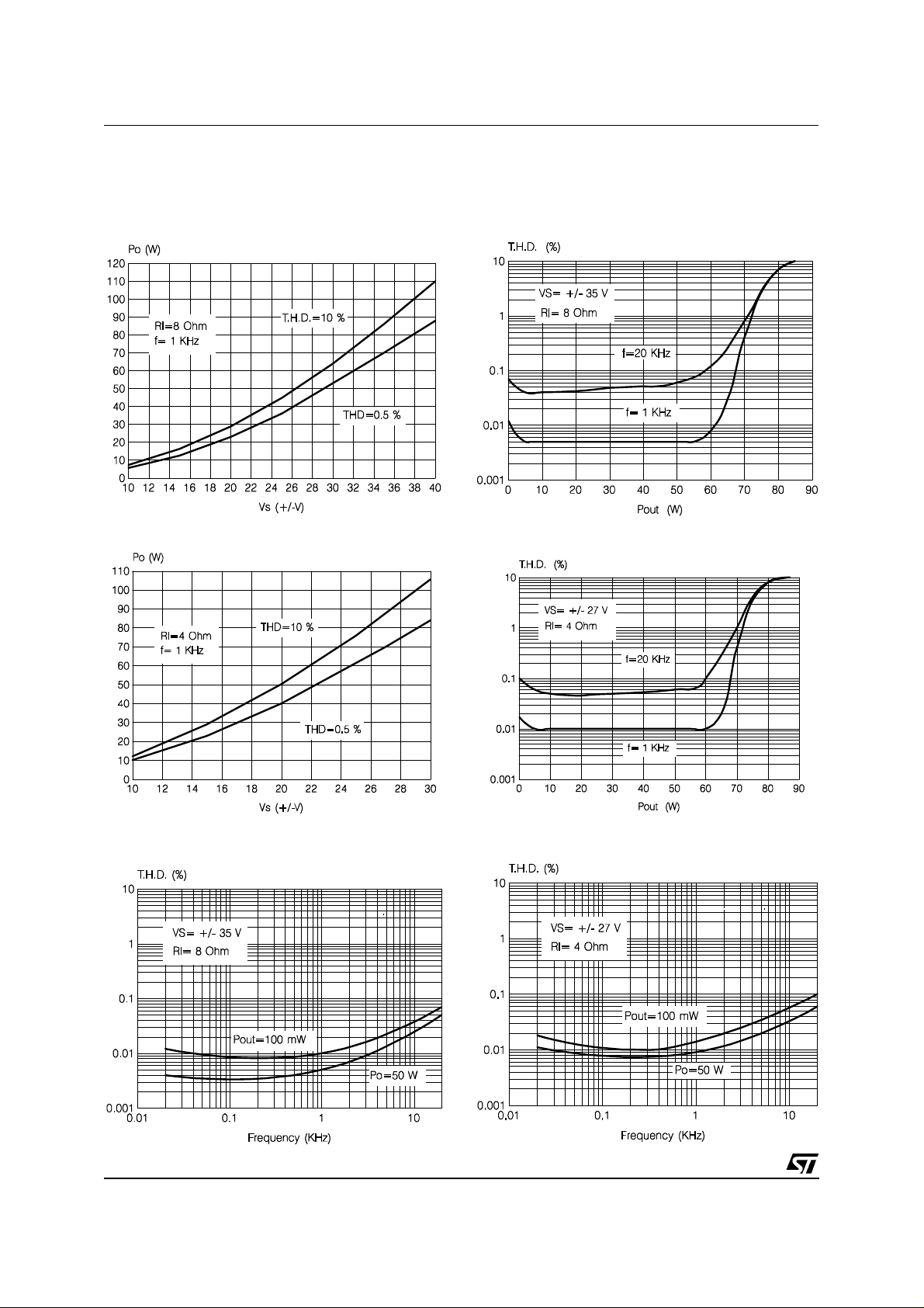
Figure 3: Output Power vs. Supply Voltage.
Figure 5: Output Power vs. Supply Voltage
Figure 4: Distortion vs. Output Power
Figure 6: Distortion vs. Output Power
Figure 7: Distortion vs. Frequency
6/17
Figure 8: Distortion vs. Frequency
Page 7
TYPICAL CHARACTERISTICS (continued)
TDA7294
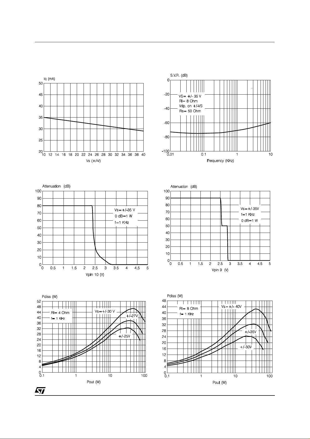
Figure 9: Quiescent Current vs. Supply Voltage
Figure 11: Mute Attenuation vs. V
pin10
Figure 10: Supply Voltage Rejection vs. Frequency
Figure 12: St-by Attenuation vs. V
pin9
Figure 13: Power Dissipation vs. Output Power
Figure 14: Power Dissipation vs. Output Power
7/17
Page 8

TDA7294
INTRODUCTION
In consumer electronics, an increasing demand
has arisen for very high power monolithic audio
amplifiers able to match, with a low cost th e performance obtained from the best discrete designs.
The task of realizing this linear integrated circuit
in conventional bipolar technology is made extremely difficult by the occurence of 2nd breakdown phenomenon. It limits the safe operating
area (SOA) of the power devices, and as a consequence, the maximum attainable output power,
especially in presence of highly reactive loads.
Moreover, full exploitation of the SOA translates
into a substantial increase in circuit and layout
complexity due to the need for sophisticated protection circuits.
To overcome these substantial drawbacks, the
use of power MOS devices, which are immune
monic distortion and good behaviour over frequency response; moreover, an accurate control
of quiescent current is required.
A local linearizing feedback, provided by differential amplifier A, is used to fullfil the above requirements, allowing a simple and effective quiescent
current setting.
Proper biasing of the power output transistors
alone is however not enough to guarantee the absence of crossover distortion.
While a linearization of the DC transfer characteristic of the stage is obtained, the dynamic behaviour of the system must be taken into account.
A significant aid in keeping the distortion contributed by the final stage as low as possible is provided by the compensation scheme, which exploits the direct connection of the Miller capacitor
at the amplifier’s output to introduce a local AC
feedback path enclosing the output stage itself.
from secondary breakdown is highly desirable.
The device described has therefore been devel-
oped in a mixed bipolar-MOS high voltage technology called BCD 100.
2) Protections
In designing a power IC, particular attention must
be reserved to the circuits devoted to protection
of the device from short circuit or overload condi-
1) Output Stage
The main design task one is confronted with while
developing an integrated circuit as a power operational amplifier, independently of the technology used, is that of realizing the output stage.
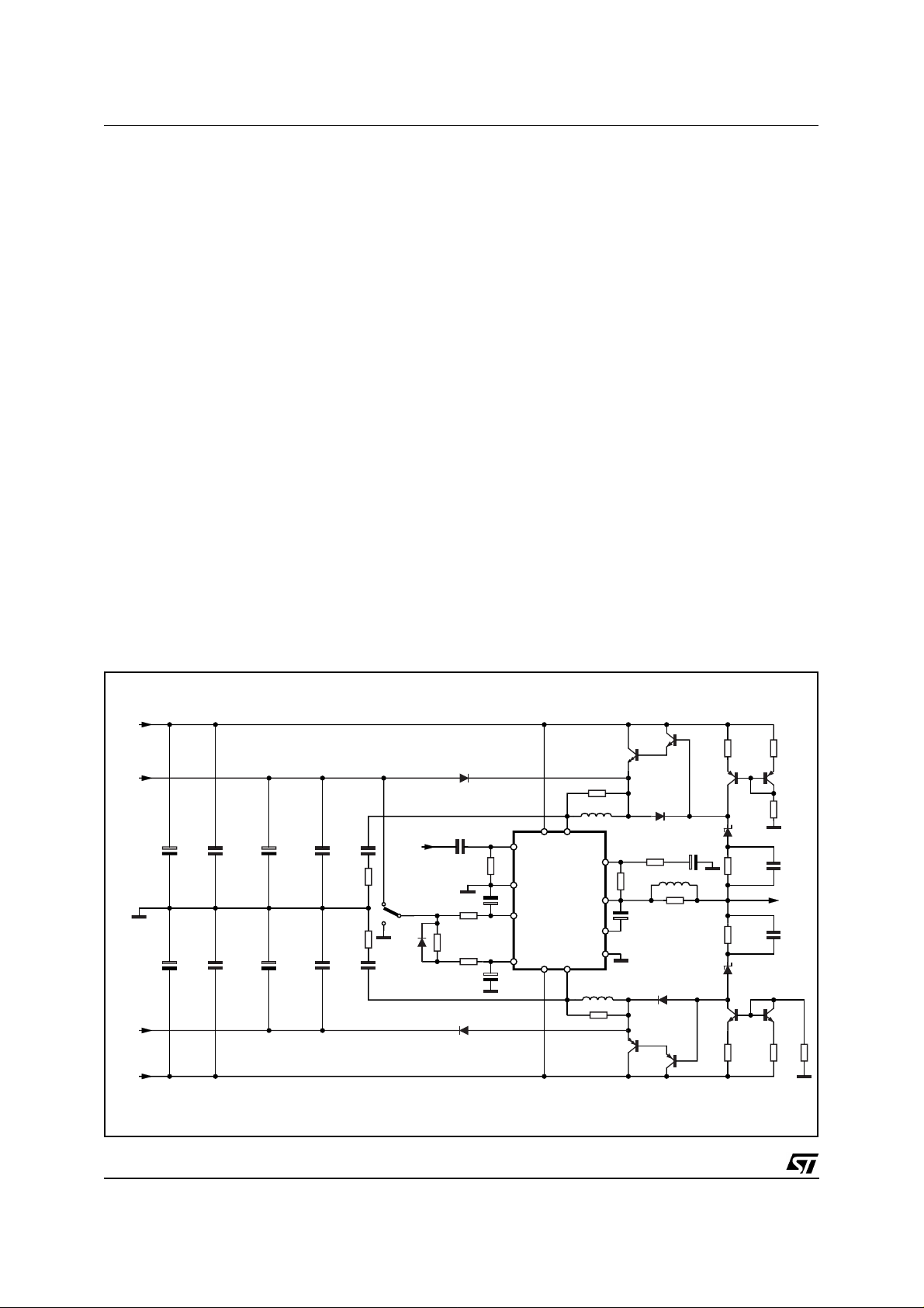
The solution shown as a principle shematic by Fig
15 represents the DMOS unity-gain output buffer
of the TDA7294.
This large-signal, high-power buffer must be capable of handling extremely high current and voltage levels while maintaining acceptably low har-
tions.
Due to the absence of the 2nd breakdown phe-
nomenon, the SOA of the power DMOS tr ansis-
tors is delimited only by a maximum dissipation
curve dependent on the duration of the applied
stimulus.
In order to fully exploit the capabilities of the
power transistors, the protection scheme imple-
mented in this device combines a conventional
SOA protection circuit with a novel local tempera-
ture sensing technique which " dynamically" con-
trols the maximum dissipation.
Figure 15: Principle Schematic of a DMOS unity-gain buffer.
8/17
Page 9

Figure 16: Turn ON/OFF Suggested Sequence
+Vs
(V)
+35
-35
-Vs
V
IN
(mV)
V
ST-BY
PIN #9
(V)
5V
TDA7294
V
MUTE
PIN #10
(V)
I
P
(mA)
V
OUT
(V)
5V
OFF
ST-BY
PLAY
MUTE MUTE
In addition to the overload protection described
above, the device features a thermal shutdown
circuit which initially puts the device into a muting
state (@ Tj = 145
o
C) and then into stand-by (@
Figure 17: Single Signal ST-BY/MUTE Control
Circuit
MUTE STBY
MUTE/
ST-BY
20K
10K 30K
1N4148
10µF10µF
D93AU014
ST-BY OFF
D93AU013
Tj = 150
o
C).
Full protection against electrostatic discharges on
every pin is included.
3) Other Features
The device is provided with both stand-by and
mute functions, independently driven by two
CMOS logic compatible input pins.
The circuits dedicated to the switching on and off
of the amplifier have been carefully optimized to
avoid any kind of uncontrolled audible transient at
the output.
The sequence that we recommend during the
ON/OFF transients is shown by Figure 16.
The application of figure 17 shows the possibility
of using only one command for both st-by and
mute functions. On both the pins, the maximum
applicable range corresponds to the operating
supply voltage.
9/17
Page 10
TDA7294
APPLICATION IN FOR MATION
HIGH-EFFI CI ENC Y
Constraints of implementing high power s olutions
are the power dissipation and the size of the
power supply. These are both due to the low efficiency of conventional AB class amplifier approaches.
Here below (figure 18) is described a circuit proposal for a high efficiency amplifier which can be
adopted for both HI-FI and CAR-RADIO applications.
The TDA7294 is a monolithic MOS power amplifier which can be oper ated at 80V supply voltage
(100V with no signal applied) while delivering output currents up to ±10 A.
This allows the use of this device as a very high
power amplifier (up to 180W as peak power with
T.H.D.=10 % and Rl = 4 Ohm); the only drawback
is the power dissipation, hardly manageable in
the above power range.
Figure 20 shows the power dissipation versus
output power curve for a c lass AB amplifier, compared with a high efficiency one.
In order to dimension the heatsink (and the power
supply), a generally used average output power
value is one tenth of the maximum output power
at T.H.D.=10 %.
From fig. 20, where the maximum power is
around 200 W, we get an average of 20 W, in this
condition, for a class AB amplifier the average
power dissipation is equal to 65 W.
The typical junction-to-case thermal resistance of
the TDA7294 is 1
avoid that, in worst case conditions, the chip tem-
perature exceedes 150
of the heatsink must be 0.038
o
C/W (max= 1.5 oC/W). To
o
C, the thermal resistance
o
C/W (@ max am-
bient temperature of 50 oC).
As the above value is pratically unreachable; a
high efficiency system is needed in those cases
where the continuous RMS output power is higher
than 50-60 W.
The TDA7294 was designed to work also in
higher efficiency way.
For this reason there are four power supply pins:
two intended for the signal part and two for the
power part.
T1 and T2 are two power transistors that only op-
erate when the output power reaches a certain
threshold (e.g. 20 W). If the output power in-
creases, these transistors are switched on during
the portion of the signal where more output volt-
age swing is needed, thus "bootstrapping" the
power supply pins (#13 and #15).
The current generators formed by T4, T7, zener
Figure 18: High Efficiency Application Circuit
+40V
+20V
C9
330nF
R1
2
PLAY
ST-BY
R2
2
C10
C8
330nF
1N4148
GND
-20V
-40V
C1
1000µF
C2
1000µF
C3
100nF
C4
100nF
C5
1000µF
C6
1000µF
100nF
100nF
INC7
D5
D1 BYW98100
C11 330nF
R16
13K
C13 10µF
R13 20K
R14 30K
R15 10K
C14
10µF
D2 BYW98100
3
4
TDA7294
9
815
10
T3
BC394
T1
BDX53A
270
L1 1µH
137
14
L2 1µH
270
BDX54A
2
6
1
D3 1N4148
R3 680
R16
13K
C15
22µF
D4 1N4148
T2
T6
BC393
C11 22µF
L3 5µH
270
R4
270
T4
BC393
Z1 3.9V
Z2 3.9V
T7
BC394
R9
270
R7
3.3K
R8
3.3K
R5
270
R6
20K
R10
270
D93AU016
T5
BC393
C16
1.8nF
OUT
C17
1.8nF
T8
BC394
R11
29K
10/17
Page 11
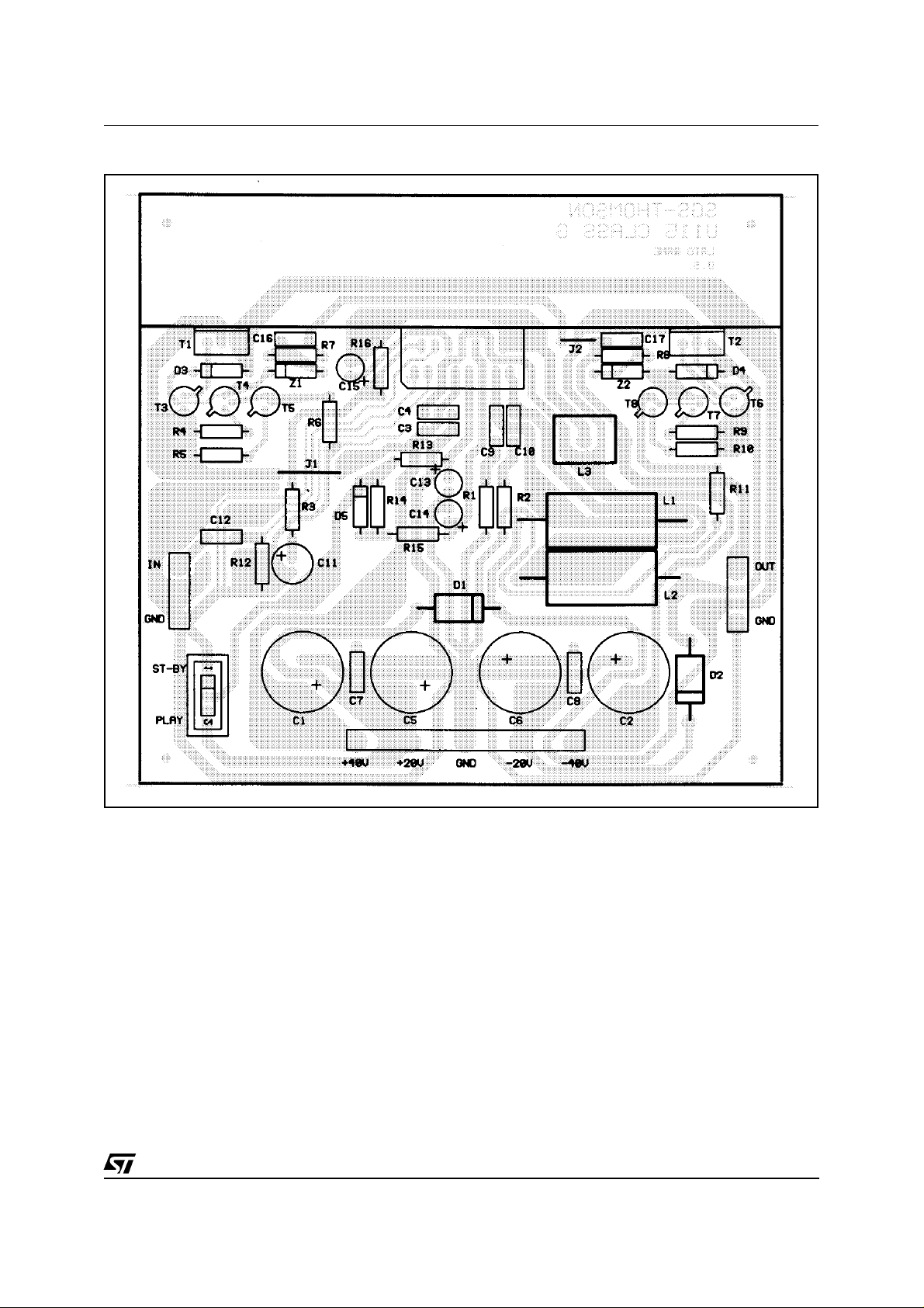
Figure 19: P.C.B. and Components Layout of the Circuit of figure 18 (1:1 scale)
TDA7294
diodes Z1,Z2 and resistors R7,R8 define the minimum drop across the power MOS transistors of
the TDA7294. L1, L2, L3 and the snubbers C9,
R1 and C10, R2 stabilize the loops formed by the
"bootstrap" circuits and the output stage of the
TDA7294.
In figures 21,22 the performances of the system
in terms of distortion and output power at various
frequencies (measured on PCB shown in fig. 19)
are displayed.
The out put powe r that the TDA729 4 in high efficiency application is able to supply at
Vs = +40V/+20V/-20V/-40V; f =1 KHz is:
- Pout = 150 W @ T.H.D.=10 % with Rl= 4 Ohm
- Pout = 120 W @ " = 1 % " " "
- Pout = 100 W @ " =10 % with Rl= 8 Ohm
- Pout = 80 W @ " = 1 % " " "
Results from efficiency measurements (4 and 8
Ohm loads, Vs = ±40V) are shown by figures 23
and 24. We have 3 curves: total power dissipa-
tion, power dissipation of the TDA7294 and
power dissipation of the darlingtons.
By considering again a maximum average
output power (music signal) of 20W, in case
of th e high eff iciency a pplication , the the rmal
resistance value needed from the heatsink is
o
C/W (Vs =±40 V and Rl= 4 Ohm).
2.2
All components (TDA7294 and power transistors
T1 and T2) can be placed on a 1.5
o
C/W heatsink,
with the power darlingtons electrically insulated
from the heatsink.
Since the total power dissipation is less than that
of a usual class AB amplifier, additional cost savings can be obtained while optimizing the power
supply, even with a high headroom.
11/17
Page 12

TDA7294
Figure 20: Power Dissipation vs. Output Power
HIGH-EFFICI ENCY
Figure 22: Distortion vs. Output Power
Figure 21: Distortion vs. Output Power
Figure 23: Power Dissipation vs. Output Power
Figure 24: Power Dissipation vs. Output Power
12/17
Page 13

TDA7294
BRIDGE APPLICATION
Another application suggestion is the BRIDGE
configuration, where two TDA7294 are used, as
shown by the schematic diagram of figure 25.
In this application, the value of the load must not
be lower than 8 Ohm for dissipation and current
capability reasons.
A suitable field of application includes HI-FI/TV
subwoofers realizations.
The main advantages offered by this solution are:
Figure 25: Bridge Application Circuit
+Vs
2200µF0.22µF
Vi
22K0.56µF
ST-BY/MUTE
20K
3
1
4
10
- High power performances with limited supply
voltage level.
- Considerably high output power even with high
load values (i.e. 16 Ohm).
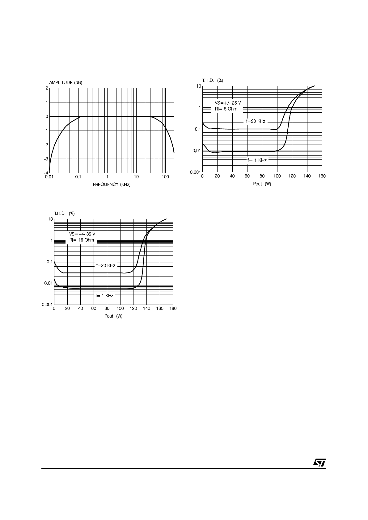
The characteristics shown by figures 27 and 28,
measured with loads respectively 8 Ohm and 16
Ohm.
With Rl= 8 Ohm, Vs = ±25V the maximum output
power obtainable is 150 W, while with Rl=16
Ohm, Vs = ±35V the maximum Pout is 170 W.
137
6
+
-
TDA7294
9
815
14
22µF
2
22K
680
22µF
1N4148
10K 30K
0.56µF 22K
22µF
9
10
TDA7294
3
1
4
15 8
+
-
137
2200µF
6
14
2
22K
-Vs
0.22µF
22µF
22K
680
D93AU015A
13/17
Page 14
TDA7294
Figure 26: Frequency Response of the Bridge
Application
Figure 28: Distortion vs. Output Power
Figure 27: Distortion vs. Output Power
14/17
Page 15

TDA7294
DIM.
Dia1 3.65 3.85 0.144 0.152
MIN. TYP. MAX. MIN. TYP. MAX.
A 5 0.197
B 2.65 0.104
C 1.6 0.063
D 1 0.039
E 0.49 0.55 0.019 0 .022
F 0.66 0.75 0.026 0.030
G 1.02 1.27 1.52 0 .040 0.050 0.060
G1 17.53 17.78 18.03 0.690 0.700 0.710
H1 19.6 0.772
H2 20.2 0.795
L 21.9 22.2 22.5 0.862 0.874 0.886
L1 21.7 22.1 22.5 0.854 0.870 0.886
L2 17.65 18.1 0.695 0.713
L3 17.25 17.5 17.75 0.679 0.689 0.699
L4 10.3 10.7 10.9 0.406 0.421 0.429
L7 2.65 2.9 0.104 0.114
M 4.25 4.55 4.85 0.167 0.179 0.191
M1 4.63 5.08 5.53 0.182 0.200 0.218
S 1.9 2.6 0.075 0.102
S1 1.9 2.6 0.075 0.102
mm inch
OUTLINE AND
MECHANICAL DATA
Multiwatt15 V
15/17
Page 16

TDA7294
DIM.
MIN. TYP. MAX. MIN. TYP. MAX.
A 5 0.197
B 2.65 0.104
C 1.6 0.063
E 0.49 0.55 0.019 0.022
F 0.66 0.75 0.026 0.030
G 1.14 1.27 1.4 0.045 0.050 0.055
G1 17.57 17.78 17.91 0.692 0.700 0.705
H1 19.6 0 .772
H2 20.2 0.795
L 20.57 0.810
L1 18.03 0.710
L2 2.54 0.100
L3 17.25 17.5 17.75 0.679 0.689 0.699
L4 10.3 10.7 10.9 0.406 0.421 0.429
L5 5.28 0.208
L6 2.38 0.094
L7 2.65 2.9 0.104 0.114
S 1.9 2.6 0.075 0.102
S1 1.9 2.6 0.075 0.102
Dia1 3.65 3.85 0.144 0.152
mm inch
OUTLINE AND
MECHANICAL DATA
Multiwatt15 H
16/17
Page 17

TDA7294
Information furnishe d is beli eved to be accu rate and reliable. However, STMicroelec tronics assumes no res ponsibility for the consequences
of use of such i nformation nor for any i nfringement of patents or ot her rights of third par ties which may result from its use. No license i s
granted by impli cation or otherwis e under any patent or patent righ ts of STMicroelect ronics. Specifica tion mentioned in this publication are
subject to change without notic e. This public ation supers edes and replaces all information prev iously supplied. STMic roelec tronic s products
are not authorized for use as critical components in life support devices or systems without express written approval of STMicroelectronics.
The ST logo is a registered trademark of STMicroelect roni cs
© 2003 STMicroelectronics – Printed in Italy – All Rights Reserved
Australia - Brazil - Canada - China - Finland - France - Germany - Hong Kong - India - Israel - Italy - Japan - Malaysia - Malta - Morocco -
Singapore - Spain - Sweden - Switzerland - United Kingdom - United States.
STMicroelectronics GROUP OF COMPANIES
http://www.st.com
17/17
 Loading...