

Page 1

N-channel 1500V - 5Ω - 4A - TO-220/TO-247
General features
V
Type
STP4N150 1500 V < 7 Ω 4A
STW4N150 1500 V < 7 Ω 4A
■ Avalanche ruggedness
■ Gate charge minimized
■ Very low intrinsic capacitances
■ High speed switching
DSS
(@Tjmax)
Description
R
DS(on)
STP4N150
STW4N150
Very high PowerMESH™ Power MOSFET
I
D
3
2
1
TO-220
TO-247
Using the well consolidated high voltage MESH
OVERLAY™ process, STMicroelectronics has
designed an advanced family of Power MOSFETs
with outstanding performances. The strengthened
layout coupled with the Company’s proprietary
edge termination structure, gives the lowest
RDS(on) per area, unrivalled gate charge and
switching characteristics.
Applications
■ Switching application
Order codes
Part number Marking Package Packaging
STP4N150 P4N150 TO-220 Tube
STW4N150 W4N150 TO-247 Tube
Internal schematic diagram
August 2006 Rev 4 1/14
www.st.com
14
Page 2

Contents STP4N150 - STW4N150
Contents
1 Electrical ratings . . . . . . . . . . . . . . . . . . . . . . . . . . . . . . . . . . . . . . . . . . . . 3
2 Electrical characteristics . . . . . . . . . . . . . . . . . . . . . . . . . . . . . . . . . . . . . 4
2.1 Electrical characteristics (curves) . . . . . . . . . . . . . . . . . . . . . . . . . . . . 6
3 Test circuit Package mechanical data . . . . . . . . . . . . . . . . . . . . . . . . . . 9
4 Package mechanical data . . . . . . . . . . . . . . . . . . . . . . . . . . . . . . . . . . . . 10
5 Revision history . . . . . . . . . . . . . . . . . . . . . . . . . . . . . . . . . . . . . . . . . . . 13
2/14
Page 3

STP4N150 - STW4N150 Electrical ratings
1 Electrical ratings
Table 1. Absolute maximum ratings
Symbol Parameter Value Unit
Drain-source voltage (VGS = 0)
DS
Drain-gate voltage (RGS = 20 kΩ)
Gate- source voltage ± 30 V
GS
Drain current (continuous) at TC = 25°C
D
Drain current (continuous) at TC = 100°C
D
(1)
Drain current (pulsed) 12 A
Total dissipation at TC = 25°C
1500 V
1500 V
4A
2.5 A
160 W
Derating factor 1 W/°C
V
I
DM
P
V
DGR
V
I
I
TOT
T
T
1. Pulse width limited by safe operating area
Operating junction temperature
j
Storage temperature
stg
-55 to 150 °C
Table 2. Thermal data
Symbol Parameter Value Unit
TO-220 TO-247
Rthj-case Thermal resistance junction-case max 0.78 °C/W
Rthj-amb Thermal resistance junction-ambient max 62.5 50 °C/W
Table 3. Avalanche characteristics
Symbol Parameter Value Unit
I
AR
E
Avalanche current, repetitive or not-repetitive
(pulse width limited by T
max)
j
Single pulse avalanche energy
AS
(starting T
= 25 °C, ID = IAR, VDD = 50 V)
j
4A
350 mJ
3/14
Page 4

Electrical characteristics STP4N150 - STW4N150
2 Electrical characteristics
(T
=25°C unless otherwise specified)
CASE
Table 4. On/off states
Symbol Parameter Test conditions Min. Typ. Max. Unit
V
(BR)DSS
I
DSS
I
GSS
V
GS(th)
R
DS(on
Drain-source
Breakdown voltage
Zero gate voltage
Drain current (V
GS
= 0)
Gate-body leakage
current (V
DS
= 0)
Gate threshold voltage
Static drain-source on
resistance
= 1 mA, VGS = 0
I
D
= Max Rating
V
DS
= Max Rating, TC = 125°C
V
DS
VGS = ± 30 V
= VGS, ID = 250 µA
V
DS
VGS = 10 V, ID = 2 A
1500 V
10
500µAµA
± 100 µA
345V
57Ω
Table 5. Dynamic
Symbol Parameter Test conditions Min. Typ. Max. Unit
(1)
g
fs
C
C
C
Forward transconductance
Input capacitance
iss
Output capacitance
oss
Reverse transfer
rss
capacitance
= 30 V , ID = 2 A
V
DS
= 25 V, f = 1 MHz,
V
DS
= 0
V
GS
3.5 S
1300
120
12
pF
pF
pF
T
d(on)
t
d(off)
Q
Q
Q
1. Pulsed: pulse duration=300µs, duty cycle 1.5%
Turn-on delay time
T
Rise time
r
Turn-off delay time
Fall time
t
f
g
Total gate charge
Gate-source charge
gs
Gate-drain charge
gd
V
R
(see Figure 18)
V
V
(see Figure 19)
4/14
= 750 V, ID = 2 A,
DD
= 4.7 Ω, V
G
= 600 V, ID = 4 A,
DD
= 10 V
GS
GS
= 10 V
35
30
45
45
30
10
9
ns
ns
ns
ns
50 nC
nC
nC
Page 5

STP4N150 - STW4N150 Electrical characteristics
Table 6. Source drain diode
Symbol Parameter Test conditions Min. Typ. Max. Unit
I
I
SDM
V
SD
Q
I
RRM
Q
I
RRM
1. Pulse width limited by safe operating area
2. Pulsed: pulse duration=300µs, duty cycle 1.5%
Source-drain current
SD
(1)
Source-drain current (pulsed)
(2)
Forward on voltage
t
Reverse recovery time
rr
Reverse recovery charge
rr
Reverse recovery current
t
Reverse recovery time
rr
Reverse recovery charge
rr
Reverse recovery current
= 4 A, VGS = 0
I
SD
= 4 A, di/dt = 100
I
SD
A/µs
= 45V
V
DD
(see Figure 18)
= 4 A, di/dt = 100
I
SD
A/µs
= 45V, Tj = 150°C
V
DD
(see Figure 18)
510
3
12
615
4
12.6
4
A
12
A
2V
ns
µC
A
ns
µC
A
5/14
Page 6
Electrical characteristics STP4N150 - STW4N150
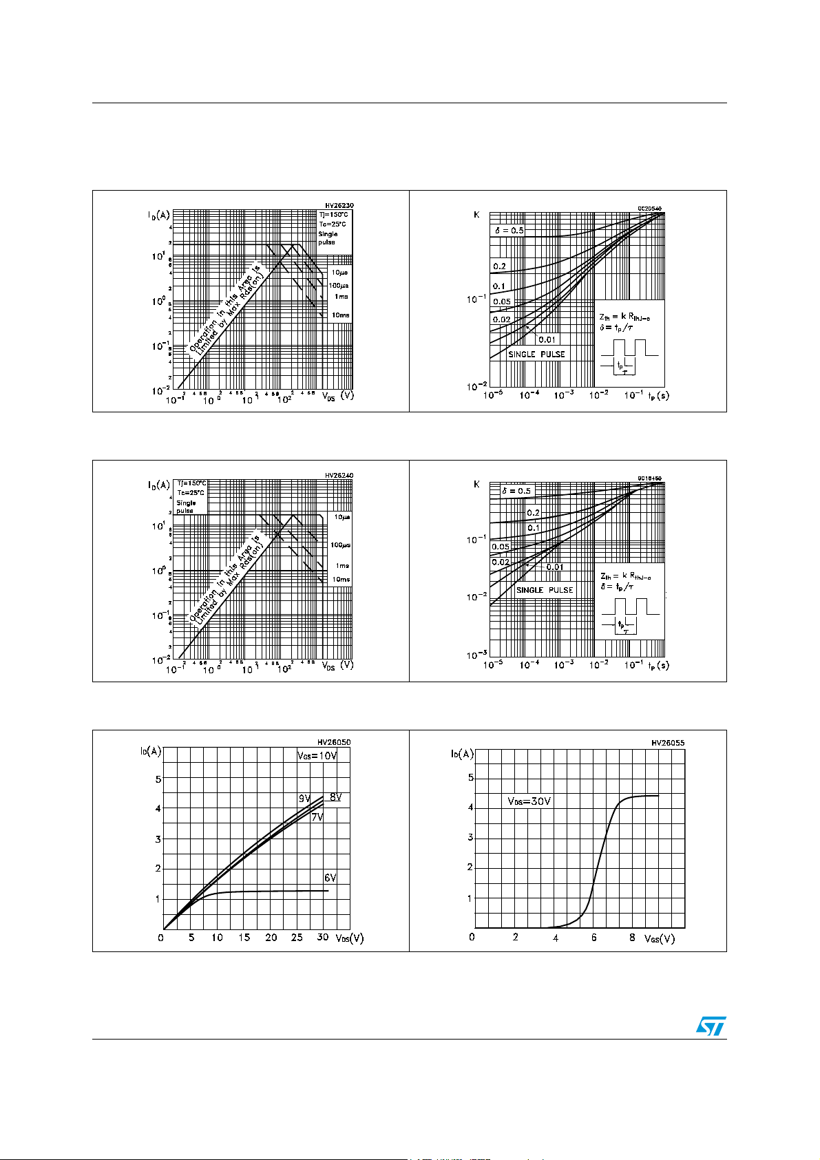
2.1 Electrical characteristics (curves)
Figure 1. Safe operating area for TO-220 Figure 2. Thermal impedance for TO-220
Figure 3. Safe operating area for TO-247 Figure 4. Thermal impedance for TO-247
Figure 5. Output characterisics Figure 6. Transfer characteristics
6/14
Page 7
STP4N150 - STW4N150 Electrical characteristics
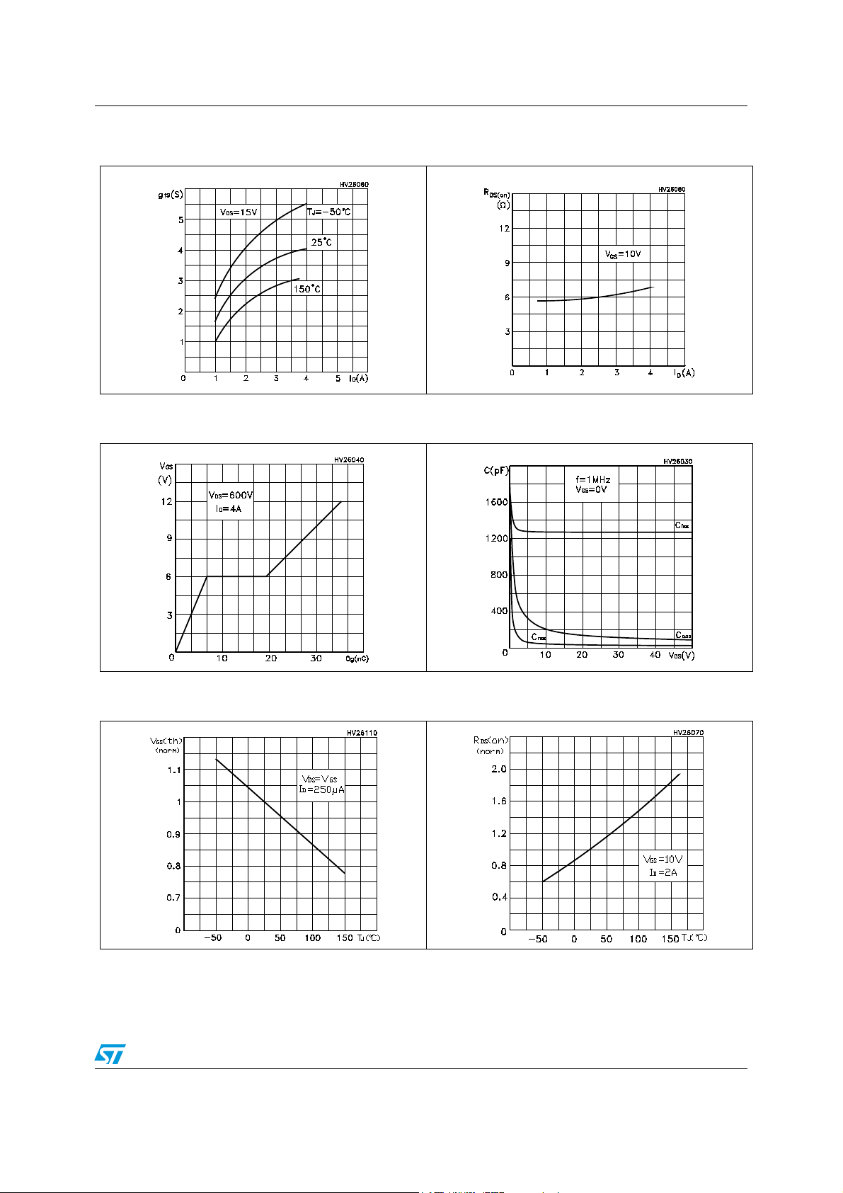
Figure 7. Transconductance Figure 8. Static drain-source on resistance
Figure 9. Gate charge vs gate-source voltage Figure 10. Capacitance variations
Figure 11. Normalized gate threshold voltage
vs temperature
Figure 12. Normalized on resistance vs
temperature
7/14
Page 8

Electrical characteristics STP4N150 - STW4N150
Figure 13. Source-drain diode forward
characteristics
Figure 15. Maximum avalanche energy vs
temperature
Figure 14. Normalized B
vs temperature
VDSS
8/14
Page 9
STP4N150 - STW4N150 Test circuit Package mechanical data
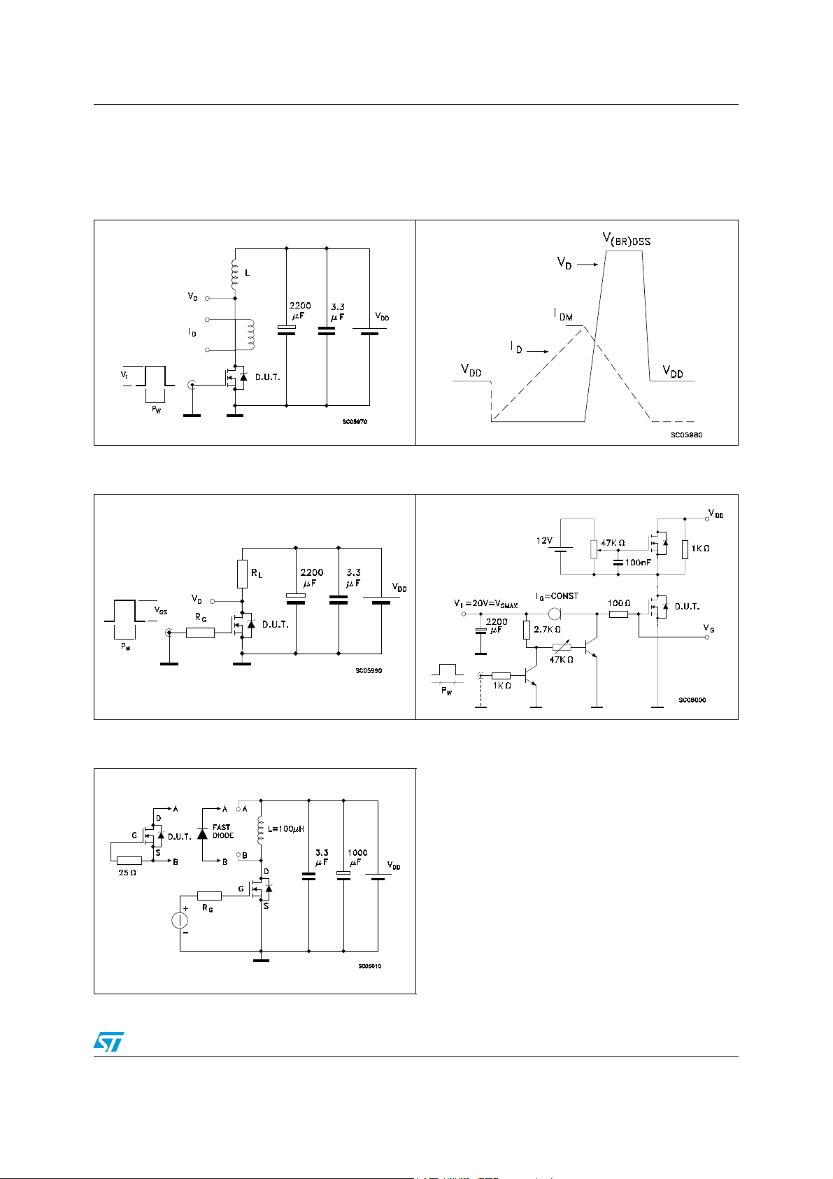
3 Test circuit Package mechanical data
Figure 16. Unclamped inductive load test
circuit
Figure 18. Switching times test circuit for
resistive load
Figure 17. Unclamped inductive waveform
Figure 19. Gate charge test circuit
Figure 20. Test circuit for inductive load
switching and diode recovery times
9/14
Page 10

Package mechanical data STP4N150 - STW4N150
4 Package mechanical data
In order to meet environmental requirements, ST offers these devices in ECOPACK®
packages. These packages have a Lead-free second level interconnect . The category of
second level interconnect is marked on the package and on the inner box label, in
compliance with JEDEC Standard JESD97. The maximum ratings related to soldering
conditions are also marked on the inner box label. ECOPACK is an ST trademark.
ECOPACK specifications are available at: www.st.com
10/14
Page 11

STP4N150 - STW4N150 Package mechanical data
DIM.
mm. inch
MIN. TYP MAX. MIN. TYP. MAX.
A 4.40 4.60 0.173 0.181
b 0.61 0.88 0.024 0.034
b1 1.15 1.70 0.045 0.066
c 0.49 0.70 0.019 0.027
D 15.25 15 .75 0.60 0.620
E 10 10.40 0.393 0.409
e 2.40 2.70 0.094 0.106
e1 4.95 5.15 0.194 0.202
F 1.23 1.32 0.048 0 .052
H1 6.20 6 .60 0.244 0.256
J1 2.40 2.72 0. 094 0 .107
L 13 14 0.511 0 .551
L1 3.50 3.93 0.137 0.154
L20 16.40 0.645
L30 28.90 1.137
øP 3.75 3 .85 0.147 0.151
Q 2 .65 2.95 0.104 0.116
TO-220 MECHANICAL DATA
11/14
Page 12

Package mechanical data STP4N150 - STW4N150
TO-247 MECHANICAL DATA
DIM.
A 4.85 5.15 0.19 0.20
A1 2.20 2.60 0.08 6 0.102
b 1.0 1.40 0.03 9 0.055
b1 2.0 2.40 0.079 0.0 94
b2 3.0 3.40 0.118 0.1 34
c 0.40 0 .80 0.015 0.03
D 19.85 20.15 0.781 0.793
E 15.45 15.75 0.608 0.620
e5.45 0.214
L 14.20 14.80 0.560 0.582
L1 3.70 4.30 0.14 0.17
L2 18 .50 0.728
øP 3.55 3.65 0.140 0.143
øR 4.50 5.50 0.177 0.216
S5.50 0.216
MIN. TYP MAX. MIN. TYP. MAX.
mm. inch
12/14
Page 13

STP4N150 - STW4N150 Revision history
5 Revision history
Table 7. Revision history
Date Revision Changes
29-Mar-2005 1 First release
07-Jul-2005 2 Removed TO-220FP
07-Oct-2005 3 Complete version
10-Aug-2006 4 New template, no content change
13/14
Page 14

STP4N150 - STW4N150
Please Read Carefully:
Information in this document is provided solely in connection with ST products. STMicroelectronics NV and its subsidiaries (“ST”) reserve the
right to make changes, corrections, modifications or improvements, to this document, and the products and services described herein at any
time, without notice.
All ST products are sold pursuant to ST’s terms and conditions of sale.
Purchasers are solely responsible for the choice, selection and use of the ST products and services described herein, and ST assumes no
liability whatsoever relating to the choice, selection or use of the ST products and services described herein.
No license, express or implied, by estoppel or otherwise, to any intellectual property rights is granted under this document. If any part of this
document refers to any third party products or services it shall not be deemed a license grant by ST for the use of such third party products
or services, or any intellectual property contained therein or considered as a warranty covering the use in any manner whatsoever of such
third party products or services or any intellectual property contained therein.
UNLESS OTHERWISE SET FORTH IN ST’S TERMS AND CONDITIONS OF SALE ST DISCLAIMS ANY EXPRESS OR IMPLIED
WARRANTY WITH RESPECT TO THE USE AND/OR SALE OF ST PRODUCTS INCLUDING WITHOUT LIMITATION IMPLIED
WARRANTIES OF MERCHANTABILITY, FITNESS FOR A PARTICULAR PURPOSE (AND THEIR EQUIVALENTS UNDER THE LAWS
OF ANY JURISDICTION), OR INFRINGEMENT OF ANY PATENT, COPYRIGHT OR OTHER INTELLECTUAL PROPERTY RIGHT.
UNLESS EXPRESSLY APPROVED IN WRITING BY AN AUTHORIZED ST REPRESENTATIVE, ST PRODUCTS ARE NOT
RECOMMENDED, AUTHORIZED OR WARRANTED FOR USE IN MILITARY, AIR CRAFT, SPACE, LIFE SAVING, OR LIFE SUSTAINING
APPLICATIONS, NOR IN PRODUCTS OR SYSTEMS WHERE FAILURE OR MALFUNCTION MAY RESULT IN PERSONAL INJURY,
DEATH, OR SEVERE PROPERTY OR ENVIRONMENTAL DAMAGE. ST PRODUCTS WHICH ARE NOT SPECIFIED AS "AUTOMOTIVE
GRADE" MAY ONLY BE USED IN AUTOMOTIVE APPLICATIONS AT USER’S OWN RISK.
Resale of ST products with provisions different from the statements and/or technical features set forth in this document shall immediately void
any warranty granted by ST for the ST product or service described herein and shall not create or extend in any manner whatsoever, any
liability of ST.
ST and the ST logo are trademarks or registered trademarks of ST in various countries.
Information in this document supersedes and replaces all information previously supplied.
The ST logo is a registered trademark of STMicroelectronics. All other names are the property of their respective owners.
© 2006 STMicroelectronics - All rights reserved
STMicroelectronics group of companies
Australia - Belgium - Brazil - Canada - China - Czech Republic - Finland - France - Germany - Hong Kong - India - Israel - Italy - Japan -
Malaysia - Malta - Morocco - Singapore - Spain - Sweden - Switzerland - United Kingdom - United States of America
www.st.com
14/14
 Loading...